

Page 1
Data Sheet
600mA LOW DROPOUT LINEAR REGULATOR AP1117M
600mA LOW DROPOUT LINEAR REGULATOR AP2317
General Description
The AP2317 is a series of low dropout three-terminal
regulators with a dropout of 1.1V at 600mA output current.
This product has been optimized for low voltage where
transient response and minimum input voltage are critical. The AP2317 provides current limit and thermal
shutdown. Its circuit includes a trimmed bandgap reference to assure output voltage accuracy to be within
±1%. On-chip thermal shutdown provides protection
against any combination of overload and ambient temperatures that would create excessive junction temperatures.
The AP2317 is available in 2.5V and 3.3V versions.
The fixed versions integrate the corresponding resistor
divider. It is also available in an adjustable version
which can set the output voltage with two external
resistors.
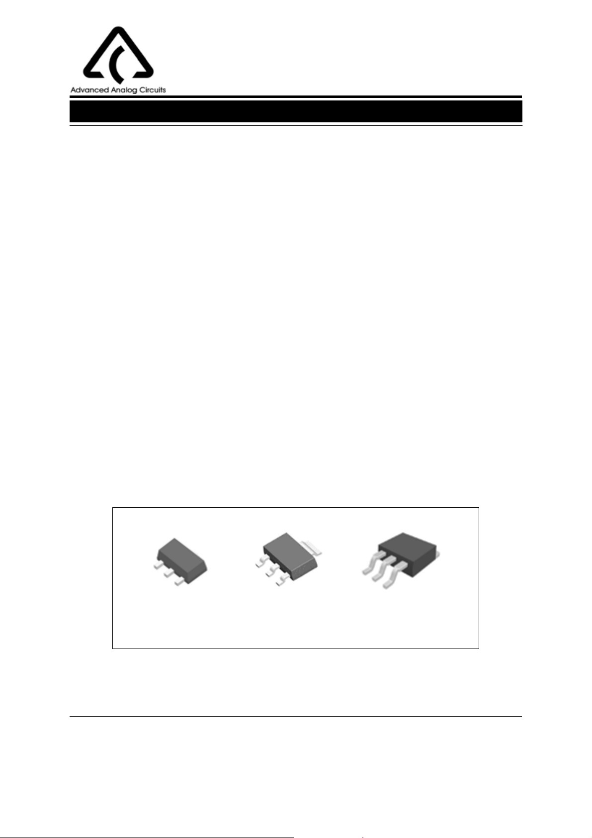
The AP2317 is available in the industry standard SOT89-3, SOT-223 and TO-263-3 (for 3.3V only) power
packages.
Features
· Low Dropout Voltage: 1.1V at 600mA Output
Current
· Output Noise from 10Hz to 10KHz: 0.003% of
V
OUT
· PSRR at I
· Output Voltage Accuracy: ± 1%
· On-chip Thermal Shutdown
· Maximum Quiescent Current
· ESD (Human Body Model): 3.5KV
· Operation Junction Temperature: -40 to 125oC
=300mA and f=120Hz: 75dB
OUT
: I
QMAX
=5mA
Applications
· DVD/CD-ROM
· USB Device
· Add-on Card
· DVD Player
· PC Motherboard
SOT-89-3 SOT-223
Figure 1. Package Types of AP2317
Mar. 2007 Rev. 1. 6 BCD Semiconductor Manufacturing Limited
1
TO-263-3
Page 2
Data Sheet
600mA LOW DROPOUT LINEAR REGULATOR AP1117M
600mA LOW DROPOUT LINEAR REGULATOR AP2317
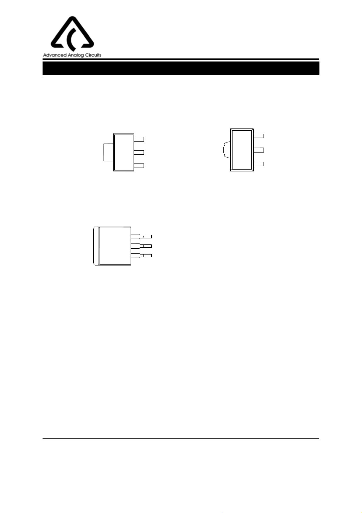
Pin Configuration
H Package
(SOT-223)
3
V
OUT
2
1
INPUT
OUTPUT
ADJ/GND
V
OUT
R Package
(SOT-89-3)
3
2
1
INPUT
OUTPUT
ADJ/GND
S Package
(TO-263-3)
3
2
1
INPUT
OUTPUT
GND
Figure 2. Pin Configuration of AP2317 (Top View)
Mar. 2007 Rev. 1. 6 BCD Semiconductor Manufacturing Limited
2
Page 3
Data Sheet
600mA LOW DROPOUT LINEAR REGULATOR AP1117M
600mA LOW DROPOUT LINEAR REGULATOR AP2317
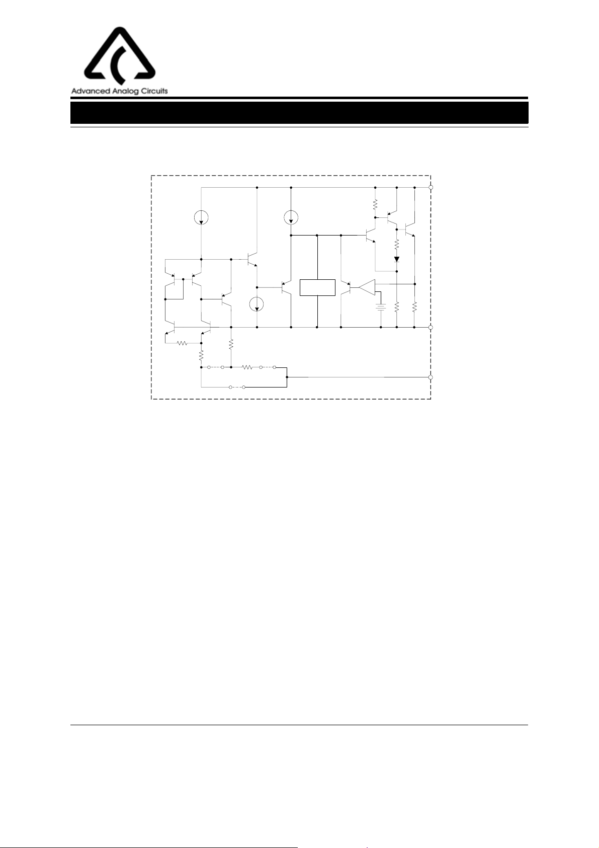
Functional Block Diagram
3
INPUT
Thermal
Protection
For Adjustable Output, disconnect A1 and A2, connect B
A1
B
For Fixed Output, connect A1 and A2, disconnect B
A2
-
+
Figure 3. Functional Block Diagram of AP2317
2
1
OUTPUT
ADJ/GND
Mar. 2007 Rev. 1. 6 BCD Semiconductor Manufacturing Limited
3
Page 4
Data Sheet
600mA LOW DROPOUT LINEAR REGULATOR AP1117M
600mA LOW DROPOUT LINEAR REGULATOR AP2317
Ordering Information
AP2317 -
Package
SOT-89-3
SOT-223
TO-263-3
Circuit Type
Package
H: SOT-223
R: SOT-89-3
S: TO-263-3
Temperature
Range
-40 to
125oC
-40 to
125oC
-40 to
125oC
E1: Lead Free
Blank: Tin Lead
TR: Tape and Reel
Blank: Tube
ADJ: Adjustable Output
2.5: Fixed Output 2.5V
3.3: Fixed Output 3.3V
Part Number Marking ID
Tin Lead Lead Free Tin Lead Lead Free
AP2317R-ADJTR AP2317R-ADJTRE1 R27A E27A Tape & Reel
AP2317R-2.5TR AP2317R-2.5TRE1 R27B E27B
AP2317R-3.3TR AP2317R-3.3TRE1 R27C E27C
AP2317H-ADJTR AP2317H-ADJTRE1 H27A EH27A
AP2317H-2.5TR AP2317H-2.5TRE1 H27B EH27B
AP2317H-3.3TR AP2317H-3.3TRE1 H27C EH27C
AP2317S-3.3 AP2317S-3.3E1 AP2317S-3.3 AP2317S-3.3E1 Tube
AP2317S-3.3TR AP2317S-3.3TRE1 AP2317S-3.3 AP2317S-3.3E1 Tape & Reel
Packing
Type
Tape & Reel
Tape & Reel
Tape & Reel
Tape & Reel
Tape & Reel
BCD Semiconductor's Pb-free products, as designated with "E1" suffix in the part number, are RoHS compliant.
Mar. 2007 Rev. 1. 6 BCD Semiconductor Manufacturing Limited
4
Page 5
Data Sheet
600mA LOW DROPOUT LINEAR REGULATOR AP1117M
600mA LOW DROPOUT LINEAR REGULATOR AP2317
Absolute Maximum Ratings (Note 1)
Parameter Symbol Value Unit
Input Voltage V
Operating Junction Temperature T
Storage Temperature Range T
Lead Temperatur e (Solder ing, 10sec) T
LEAD
IN
J
STG
15 V
150
-65 to 150
260
o
C
o
C
o
C
SOT-223 120
o
Thermal Resistance (Note 2)
θ
JA
SOT-89-3 165
C/W
TO-263-3 80
ESD (Human Body Model) ESD 3500 V
ESD (Machine Model) ESD 400 V
Note 1: Stresses greater than those listed under "Absolute Maximum Ratings" may cause permanent damage to the device.
These are stress ratings only, and functional operation of the device at these or any other conditions beyond those indicated
under "Recommended Operating Conditions" is not implied. Exposure to "Absolute Maximum Ratings" for extended periods
may affect device reliability.
Note 2: Absolute maximum ratings indicate limits beyond which damage to the component may occur. Electrical specifications do not apply when operating the device outside of its operating ratings. The maximum allowable power dissipation is a
function of the maximum junction temperature, T
perature, T
TA)/θ
The maximum allowable power dissipation at any ambient temperature is calculated using: P
A.
Exceeding the maximum allowable power dissipation will result in excessive die temperature, and the regulator will
JA.
the junction-to-ambient thermal resistance, θ
J(max),
and the ambient tem-
JA,
=(T
D(max)
J(max)
go into thermal shutdown.
-
Recommended Operating Conditions
Parameter Symbol Min Max Unit
Input Voltage
Operating Junction Temperature Range T
V
IN
J
-40 125
Mar. 2007 Rev. 1. 6 BCD Semiconductor Manufacturing Limited
5
12 V
o
C
Page 6

Data Sheet
600mA LOW DROPOUT LINEAR REGULATOR AP1117M
600mA LOW DROPOUT LINEAR REGULATOR AP2317
Electrical Characteristics
V
REF
V
OUT
∆V
OUT
∆V
OUT
V
DROP
I
LIMIT
I
ADJ
∆I
ADJ
I
LOAD
(MIN)
I
Q
AP2317-ADJ I
10mA≤I
OUT
P≤maximum power dissipation
AP2317-2.5 I
10mA≤I
OUT
AP2317-3.3 I
10mA≤I
OUT
AP2317-ADJ
=10mA, 1.5V≤VIN-V
I
OUT
AP2317-2.5
=10mA, 1.5V≤VIN-V
I
OUT
AP2317-3.3
=10mA, 1.5V≤VIN-V
I
OUT
AP2317-ADJ
(VIN-V
OUT
AP2317-2.5
(V
IN-VOUT
AP2317-3.3
(V
IN-VOUT
∆V
=1%, I
REF
(VIN-V
OUT
1.4V≤(VIN-V
1.5V≤(VIN-V
VIN=V
OUT
f=120Hz, C
(V
IN-VOUT
=125oC, 1000hrs.
T
A
TA=25oC, 10Hz≤f≤10KHz
=10mA, VIN-V
OUT
≤600mA, 1.4V≤V
=10mA, VIN=4.5V, TJ=25oC
OUT
≤600mA, 3.9V≤ V
=10mA, VIN=5.0V, TJ=25oC
OUT
≤ 600mA, 4.75V≤VIN≤10V
)=2V, 10mA≤I
)=2V, 10mA≤I
)=2V, 10mA≤ I
=0.6A
OUT
)=2V
)≤10, 10mA≤I
OUT
)≤10V (ADJ only)
OUT
+1.25V
=22µF Tan talum
OUT
)=3V, I
OUT
=300mA
OUT
OUT
OUT
OUT
OUT
OUT
OUT
IN -VOUT
≤10V
IN
≤10V
≤10V
≤10V
≤600mA
≤600mA
≤600mA
≤600mA
OUT
=2V, TJ=25oC
≤8V
o
C to 125oC
1.238
1.250
1.262
1.225
1.250
1.270
2.475
2.450
3.267
3.235
2.5
2.5
3.3
3.3
2.525
2.550
3.333
3.365
0.035 0.2 %
1 6 mV
1 6 mV
0.2 0.4 %
1 10 mV
1 10 mV
1.1 1.3
0.75 0.9
60 120
0.2 5
1.7 5 mA
5
60 75 dB
0.3 %
0.003 %
150
25
V
V
V
V
A
µA
µA
mA
o
C
o
C
Operating Conditions: VIN≤10V, TJ=25oC, unless otherwise specified. (P≤maximum power dissip ation)
Limits appearing in Boldface type apply over the entire junction temperature range for operation, -40
Parameter Symbol Conditions Min Ty p Max Unit
Reference Voltage
Output Voltage
Line Regulation
Load Regulation
Dropout Voltage
Current Limit
Adjust Pin Current
Adjust Pin Current
Change
Minimum Load
Current
Quiescent Current
Ripple Rejection PSRR
Temperature Stability 0.5 %
Long-Term Stability
RMS Output Noise
(% of V
Thermal Shutdown Junction Temperature
Thermal Shutdown
Hysteresis
OUT
)
Mar. 2007 Rev. 1. 6 BCD Semiconductor Manufacturing Limited
6
Page 7

Data Sheet
600mA LOW DROPOUT LINEAR REGULATOR AP1117M
600mA LOW DROPOUT LINEAR REGULATOR AP2317
Typical Performance Characteristics
15
10
5
0
-5
Line Regulation (mV)
-10
-15
-40 -20 0 20 40 60 80 100 120 140
Junction Temperature (oC)
Figure 4. Line Regulation vs. Junction Temperature
1.270
1.265
1.260
1.255
1.250
1.245
1.240
Reference Voltage (V)
1.235
1.230
1.225
1.220
-40 -20 0 20 40 60 80 100 120 140
AP2317-ADJ
V
=4.8V, I
IN
OUT
=10mA
Junction Temperature (oC)
20
15
10
5
0
Load Regulation (mV)
-5
-10
-40 -20 0 20 40 60 80 100 120 140
Junction Temperature (oC)
Figure 5. Load Regulation vs. Junction Temperature
3.400
3.375
3.350
3.325
3.300
3.275
3.250
3.225
3.200
Output Voltage (V)
3.175
3.150
3.125
3.100
-40 -20 0 20 40 60 80 100 120 140
AP2317-3.3
V
=4.8V, I
OUT
=10mA
IN
Junction Temperature (oC)
Figure 6. Reference Voltage vs. Junction Temperature
Figure 7. Output Voltage vs. Junction Temperature
Mar. 2007 Rev. 1. 6 BCD Semiconductor Manufacturing Limited
7
Page 8

Data Sheet
600mA LOW DROPOUT LINEAR REGULATOR AP1117M
600mA LOW DROPOUT LINEAR REGULATOR AP2317
Typical Performance Characteristics (Continued)
3
2
1
0
Minimum Load Current (mA)
-1
-2
-40 -20 0 20 40 60 80 100 120 140
AP2317-ADJ
Junction Temperature (oC)
Figure 8. Minimum Load Current vs. Junction Temperature
1.40
1.35
1.30
1.25
1.20
1.15
1.10
1.05
1.00
0.95
Dropout Voltage (V)
0.90
T
0.85
0.80
0.75
0.70
0 100 200 300 400 500 600
T
=0oC
J
T
=25oC
J
=125oC
J
TJ=-40oC
Output Current (mA)
100
90
80
70
60
50
40
30
Adjust Pin Current (µA)
20
10
0
-40 -20 0 20 40 60 80 100 120 140
AP2317-ADJ
=4.8V, I
V
IN
OUT
=10mA
Junction Temperature (oC)
Figure 9. Adjust Pin Current vs. Junction Temperature
5.0
4.5
4.0
3.5
3.0
2.5
Power (W)
2.0
1.5
1.0
0.5
0.0
20 40 60 80 100 120 140
Case Temperature (oC)
SOT-89-3
Figure 10. Dropout Voltage vs. Output Current
Figure 11. Maximum Power Dissipation
Mar. 2007 Rev. 1. 6 BCD Semiconductor Manufacturing Limited
8
Page 9

Data Sheet
600mA LOW DROPOUT LINEAR REGULATOR AP1117M
600mA LOW DROPOUT LINEAR REGULATOR AP2317
Typical Performance Characteristics (Continued)
0.2
0.1
0
(0.1V/Div)
OUT
-0.1
∆V
5.8
5.3
4.8
(0.5V/Div)
IN
4.3
V
3.8
Time (20µs/Div)
Figure 12. Line Transient Response
(Conditions: VIN=4.8 to 5.8V, V
C
80
70
60
50
40
PSRR (dB)
30
20
10
10 100 1k 10k 100k
=1µF, C
IN
Frequency (Hz)
OUT
=3.33V, I
OUT
=10µF)
100
(50mV/Div)
OUT
∆V
(0.3A/Div)
-0.3
OUT
I
-0.6
(Conditions: V
=0.1A,
OUT
Current Limit (A)
50
0
-50
0.6
0.3
0
0.01A
Time (10µs/Div)
Figure 13. Load Transient Response
=4.8V, V
IN
1.2
1.1
1.0
0.9
0.8
0.7
0.6
0.5
0.4
0.3
0.2
0.1
0.0
-40 -20 0 20 40 60 80 100 120 140
=3.33V, I
OUT
CIN=C
OUT
Junction Temperature (oC)
OUT
=10µF)
=0.01 to 0.6A,
Figure 14. PSRR vs. Frequency
Figure 15. Current Limit vs. Junction Temperature
Mar. 2007 Rev. 1. 6 BCD Semiconductor Manufacturing Limited
9
Page 10

Data Sheet
600mA LOW DROPOUT LINEAR REGULATOR AP1117M
600mA LOW DROPOUT LINEAR REGULATOR AP2317
Typical Applications
V
V
IN
IN
=11V
=5.3V
10µF
10µF
AP2317-ADJ
V
++
IN
V
OUT
ADJ
9V at 0.6A
22µF
R1
160Ω
R2
V
1kΩ
AP2317-3.3
V
++
IN
V
OUT
GND
OUT=VREF
3.3V at 0.6A
22µF
* ( 1+R2/R1) + I
ADJ
* R2
Figure 16. Typical Applications of AP2317
Mar. 2007 Rev. 1. 6 BCD Semiconductor Manufacturing Limited
10
Page 11

Data Sheet
600mA LOW DROPOUT LINEAR REGULATOR AP1117M
600mA LOW DROPOUT LINEAR REGULATOR AP2317
Mechanical Dimensions
SOT-89-3 Unit: mm(inch)
)
)
)
5
6
7
3
5
6
0
1
1
.
.
.
0
0
0
(
(
(
0
0
0
0
5
5
9
9
2
.
.
.
0
4
3
0.360(0.014)
0.520(0.020)
4.400(0.173)
1.630(0.064)
1.830(0.072)
1.400(0.055)*
)
7
4
0
.
0
(
0
0
2
.
1
3.000(0.118)
R0.200(0.008)
4.600(0.181)
2
3
.
2
6
.
0.360(0.014)
0.480(0.019)
0.440(0.017)
0.560(0.022)
0
0
0
.
0
.
0
0
0
0
0
(
0
)
0
0
(
0
.
0
0
)
0
3
.
0
7
(
6
0
(
0
.
1
9
)
1
2
.
0
0
)
3
°
1.400(0.055)
1.600(0.063)
0.360(0.014)
0.440(0.017)
°
0
1
3
°
°
0
1
R0.150(0.006)
Mar. 2007 Rev. 1. 6 BCD Semiconductor Manufacturing Limited
11
Page 12

Data Sheet
600mA LOW DROPOUT LINEAR REGULATOR AP1117M
600mA LOW DROPOUT LINEAR REGULATOR AP2317
Mechanical Dimensions (Continued)
SOT-223 Unit: mm(inch)
6.300(0.248)
6.700(0.264)
2.900(0.114)
3.100(0.122)
0.900(0.035)
MIN
0.250(0.010)
2
.
0
3
.
0
0
1
0
.
0
(
0
5
1
0
.
0
(
0
5
)
)
4
6.700(0.264)
7.300(0.287)
1.750(0.069)
TYP
2.300(0.091)
1.500(0.059)
1.700(0.067)
TYP
0.020(0.001)
0.100(0.004)
4.500(0.177)
4.700(0.185)
3.300(0.130)
3.700(0.146)
0.610(0.024)
0.810(0.032)
1.520(0.060)
1.800(0.071)
0°
10°
Mar. 2007 Rev. 1. 6 BCD Semiconductor Manufacturing Limited
12
Page 13

Data Sheet
600mA LOW DROPOUT LINEAR REGULATOR AP1117M
600mA LOW DROPOUT LINEAR REGULATOR AP2317
Mechanical Dimensions (Continued)
TO-263-3 Unit: mm(inch)
1
.
0
(
0
7
0
.
4
0
2
8
.
4
7
0
°
)
)
0
0
8
4
3
3
.
.
0
0
(
(
0
0
5
4
6
6
.
.
9
8
2.540(0.100)
)
0
6
)
0
9
1
.
0
(
9.650(0.380)
10.290(0.405)
8.840(0.348)
3°
1.270(0.050)
1.390(0.055)
1
4
5
1
1.150(0.045)
1.390(0.055)
0.510(0.020)
0.990(0.039)
2.540(0.100)
1.150(0.045)
1.390(0.055)
7°
0.020(0.001)
0.250(0.010)
2.640(0.104)
)
1
8
5
.
0
(
0
6
7
.
2
6
.
0
(
0
4
7
.
)
0
)
)
4
6
9
0
0
1
.
.
0
0
(
(
0
0
9
9
3
6
.
.
2
2
3°
0.380(0.015)
0°
6°
2.700(0.106)
0.360(0.014)
0.400(0.016)
2
8
7°
2
°
°
.
0
0
2
8
0
.
0
(
2.540(0.100)
7
)
7.420(0.292)
)
0
2
2
.
0
(
0
0
6
.
5
7.980(0.314)
2.540(0.100)
Mar. 2007 Rev. 1. 6 BCD Semiconductor Manufacturing Limited
13
Page 14

http://www.bcdsemi.com
IMPORTANT NOTICE
BCD Semiconductor Manufacturing Limited reserves the right to make changes without further notice to any products or specifications herein. BCD Semiconductor Manufacturing Limited does not assume any responsibility for use of any its products for any
particular purpose, nor does BCD Semiconductor Manufacturing Limited assume any liability arising out of the application or use
of any its products or circuits. BCD Semiconductor Manufacturing Limited does not convey any license under its patent rights or
other rights nor the rights of others.
MAIN SITE
BCD Semiconductor Manufacturing Limited
- Wafer Fab
Shanghai SIM-BCD Semiconductor Manufacturing Limited
800, Yi Shan Road, Shanghai 200233, China
Tel: +86-21-6485 1491, Fax: +86-21-5450 0008
REGIONAL SALES OFFICE
Shenzhen Office
Shanghai SIM-BCD Semiconductor Manufacturing Co., Ltd. Shenzhen Office
Advanced Analog Circuits (Shanghai) Corporation Shenzhen Office
Room E, 5F, Noble Center, No.1006, 3rd Fuzhong Road, Futian District, Shenzhen 518026, China
Tel: +86-755-8826 7951
Fax: +86-755-8826 7865
BCD Semiconductor Manufacturing Limited
- IC Design Group
Advanced Analog Circuits (Shanghai) Corporation
8F, Zone B, 900, Yi Shan Road, Shanghai 200233, China
Tel: +86-21-6495 9539, Fax: +86-21-6485 9673
Taiwan Office
BCD Semiconductor (Taiwan) Company Limited
4F, 298-1, Rui Guang Road, Nei-Hu District, Taipei,
Taiwan
Tel: +886-2-2656 2808
Fax: +886-2-2656 2806
USA Office
BCD Semiconductor Corporation
30920 Huntwood Ave. Hayward,
CA 94544, U.S.A
Tel : +1-510-324-2988
Fax: +1-510-324-2788
 Loading...