

Page 1
AP2280
Single Channel Slew Rate Controlled Load Switch
Features
• Wide input voltage range: 1.5V – 6V
• Low R
• Turn-on slew rate controlled
• AP2280-1: 100us turn-on rise time
• AP2280-2: 1ms turn-on rise time
• Very low turn-on quiescent current: << 1uA
• Fast load discharge pin
• Temperature range -40ºC to 85°C
• SOT25 and DFN2018-6: Available in “Green” Molding
Compound (No Br, Sb)
• Lead Free Finish/ RoHS Compliant (Note 1)
: 80mΩ typical @ 5V
DS(ON)
Applications
• Smart Phones
• Personal Digital Assistant (PDA)
• Cell Phones
• GPS Navigators
• Bluetooth Headsets
• PMP/MP4
• Notebook and Pocket PC
Description
The AP2280 slew rate controlled load switch is a si ngle P -channel
MOSFET power switch designed for high-side load-switching or
power distribution applications. The MOSFET has a typical
of 80mΩ at 5V, allowing increased load current handling
R
DS(ON)
capability with a low forward voltage drop. The turn-on slew rate of
the device is controlled internally to reduce turn-on inrush current.
The AP2280 load switch is designed to operate from 1.5V t o 6.0V,
making it ideal for 1.8V, 2.5V, 3.3V, and 5V systems. The typical
quiescent supply current is only 0.004uA, making it ideal for
battery powered distribution system where the power
consumption is a concern.
Ordering Information
Turn- on rise time
1 : 100us
2 : 1ms
AP2280 - X XX G - 7
Package
W : SOT25
FM : DFN2018-6
Green
G : Green
Packing
7 : Tape & Reel
Device
Package
Code
Packaging
(Note 2)
Quantity Part Number Suffix
AP2280-1WG-7 W SOT25 3000/Tape & Reel -7
AP2280-2WG-7 W SOT25 3000/Tape & Reel -7
AP2280-1FMG-7 FM DFN2018-6 3000/Tape & Reel -7
AP2280-2FMG-7 FM DFN2018-6 3000/Tape & Reel -7
Notes: 1. EU Directive 2002/95/EC (RoHS). All applicable RoHS exemptions applied. Please visit our website at
http://www.diodes.com/products/lead_free.html
2. Pad layout as shown on Diodes Inc. suggested pad layout document AP02001, which can be found on our website at
http://www.diodes.com/datasheets/ap02001.pdf.
.
7” Tape and Reel
AP2280 Rev. 6 1 of 12 FEBRUARY 2009
www.diodes.com © Diodes Incorporated
Page 2
Single Channel Slew Rate Controlled Load Switch
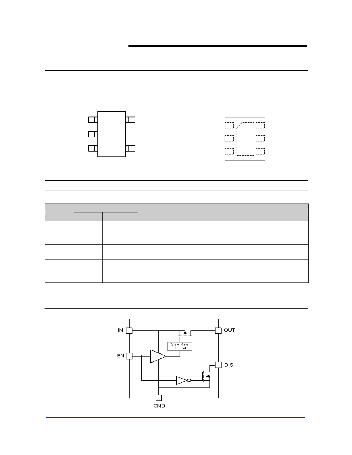
Pin Assignments
(1) SOT25 (2) DFN2018-6
GND
OUT IN
Pin Description
Pin Name
DIS 1 3
GND 2 2 Ground.
OUT
IN
EN 5 4 Enable input, active high
( Top View )
DIS
1
2
Pin Number
SOT25 DFN2018-6
3 1
4 5, 6
5
EN
43
Discharge pin. If DIS pin is tied to OUT pin externally, the output voltage
will be discharged to ground when disabled.
Voltage output pin. This is the pin to the P-channel MOSFET drain.
Bypass to ground through a 0.1uF capacitor.
Voltage input pin. This is the pin to the P-channel MOSFET source.
Bypass to ground through a 1µF capacitor.
( Top View )
OUT
GND
DIS
Description
1
2
3
AP2280
6
IN
5
IN
4
EN
Block Diagram
AP2280 Rev. 6
2 of 12 FEBRUARY 2009
www.diodes.com © Diodes Incorporated
Page 3
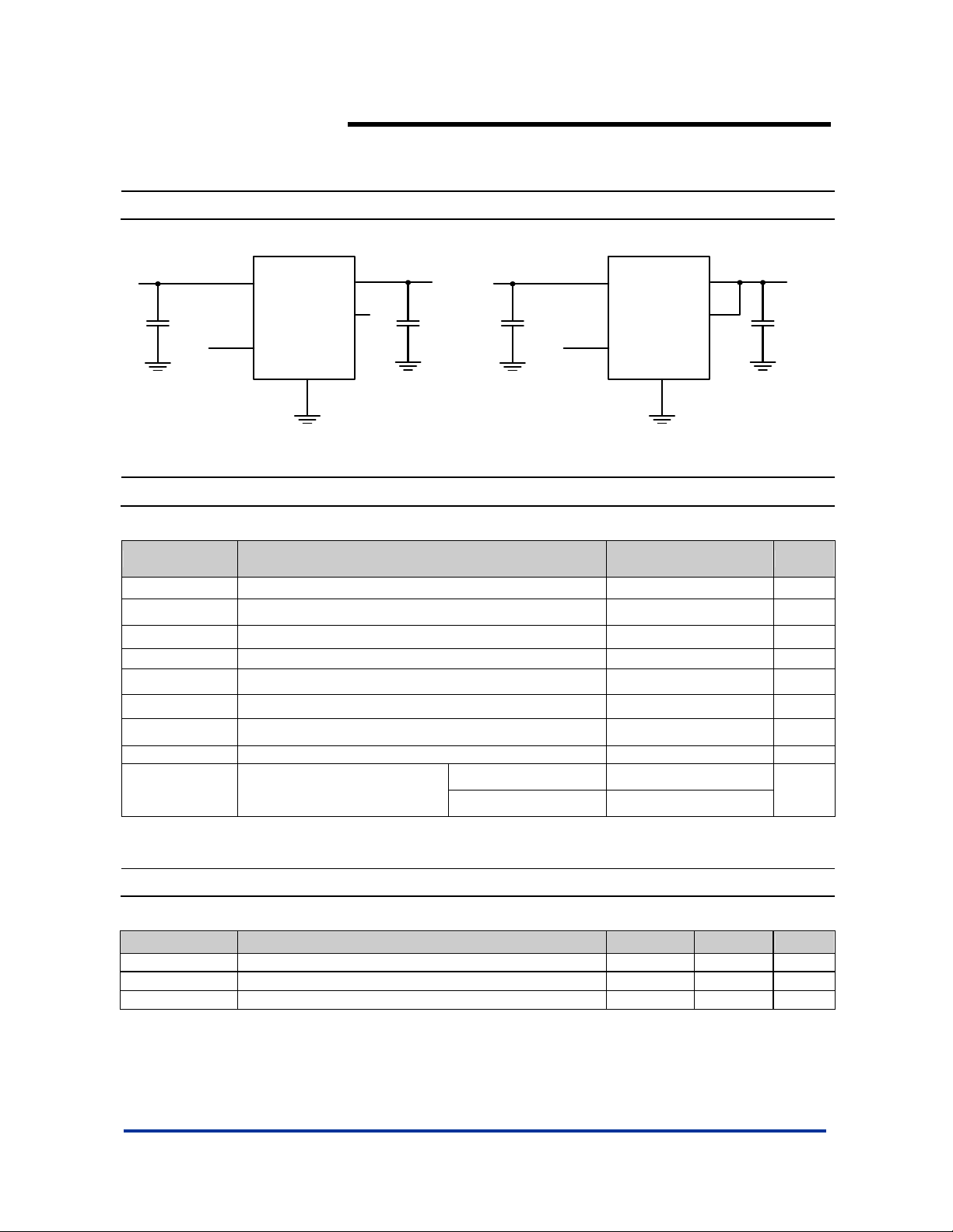
T ypical Application Circuits
V
IN
IN
OUT
AP2280
Single Channel Slew Rate Controlled Load Switch
V
OUT
V
IN
IN
OUT
V
OUT
1uF
Enable
EN
GND
DIS
0.1uF
1uF
Enable
EN
DIS
GND
For applications without output discharge For applications with output discharge
Absolute Maximum Ratings
Symbol Parameter Ratings Units
ESD HBM Human Body Model ESD Protection 4 KV
ESD MM Machine Model ESD Protection 400 V
VIN Input Voltage 6.5 V
V
Output Voltage VIN + 0.3
OUT
VEN Enable Voltage 6.5 V
I
Maximum Continuous Load Current 2 A
load
T
Maximum Junction Temperature 125 °C
J(max)
TST Storage Temperature Range -65 ~ 150 °C
SOT25 (Note 3, 5) 750
PD Power Dissipation
DFN2018-6 (Note 3, 6) 1260
Notes: 3. Ratings apply to ambient temperature at 25°C
Recommended Operating Conditions
Symbol Parameter Min Max Units
V
IN
I
OUT
T
A
Notes: 4. Maximum output current depends on application conditions. Please refer to the application note section.
Input voltage 1.5 6.0 V
Output Current (Note 4) 0 2.0 A
Operating Ambient Te mperature -40 85
0.1uF
V
mW
°C
AP2280 Rev. 6
3 of 12 FEBRUARY 2009
www.diodes.com © Diodes Incorporated
Page 4
⎯
μ
)
AP2280
Single Channel Slew Rate Controlled Load Switch
Electrical Characteristics
= 25oC, V
(T
A
Symbol Parameters Test Conditions Min Typ. Max Unit
I
Q
I
SHDN
I
LEAK
R
DS(ON)
V
IL
V
IH
I
SINK
T
D(ON)
T
ON
T
D(OFF)
R
DISCH
θ
JA
θ
JC
Notes: 5. Test condition for SOT25: Device mounted on FR-4 substrate PC board, with minimum recommended pad layout.
6. Test condition for DFN2018-6: Device mounted on FR-4 2-layer board, 2oz copper, with minimum recommended pad on top layer and 3 vias to
bottom layer 1.0"x1.4" ground plane.
AP2280 Rev. 6
= VEN = 5.0V, unless otherwise stated)
IN
Input Quiescent Current VEN = VIN, I
Input Shutdown Current VEN = 0V, OUT open
Input Leakage Current VEN = 0V, OUT grounded
V
= 5.0V 80 105 m
IN
Switch on-resistance
VIN = 3.3V 92 120 m
VIN = 1.8V 150 200 m
OUT
= 0
⎯
⎯
0.004 1
0.004 1
0.01 1
VIN = 1.5V 200 250 m
EN Input Logic Low Voltage VIN = 1.5V to 6V 0.4 V
1.4 V
1.7 V
⎯
1
1
100 150
1000 1500
0.4 1
EN Input Logic High Voltage
EN Input leakage V
Output turn-on delay time
Output turn-on rise time
Output turn-off delay time
1.5V ≤ V
≤ 2.7V
IN
2.7V < VIN < 5.25V 1.6 V
VIN ≥ 5.25V
= 5V
EN
R
=10Ω
load
AP2280-1, R
AP2280-2, R
R
=10Ω
load
load
load
=10Ω
=10Ω
Discharge FET on-resistance VEN = GND 20 40
Thermal Resistance Junction-to-Ambient
Thermal Resistance Junction-to-case
4 of 12 FEBRUARY 2009
SOT25 (Note 5) 160
DFN2018-6 (Note 6
93
SOT25 (Note 5) 38
DFN2018-6 (Note 6) 41
www.diodes.com © Diodes Incorporated
μA
μA
μA
μS
μS
μS
μS
o
C/W
o
C/W
A
Page 5

Single Channel Slew Rate Controlled Load Switch
Typical Performance Characteristics
AP2280
Quiescent Current vs. Input Voltage
0.01
0.008
0.006
0.004
0.002
Quiescent Current (uA)
0
1.0 2.0 3.0 4.0 5.0 6.0
Input Voltag e (V)
R
vs. Input Voltage
DS(ON)
300.00
250.00
200.00
(m)
150.00
DS(ON)
R
100.00
50.00
1.522.533.544.555.56
Input Voltage (V)
I=100mA
I=500mA
I=1A
I=2A
Quiescent Current vs. Temperature
0.020
0.015
0.010
0.005
Quiescent Current (uA)
0.000
-40 -20 0 20 40 60 80 100
VIN=1.8V
VIN=3.3V
VIN=5.0V
Temperature (0C)
R
vs. Temperature
DS(ON)
200.00
180.00
160.00
140.00
120.00
(m)
100.00
80.00
DS(ON)
60.00
R
40.00
20.00
0.00
-50 -25 0 25 50 75 100
VIN =1.8V
VIN =3.3V
VIN =5V
Temperature (0C)
ENABLE Threshold vs. Input Voltage
1.8
1.6
1.4
1.2
1
0.8
0.6
ON/OFF Threshold (V)
0.4
1.522.533.544.555.5
Input Voltage (V)
AP2280 Rev. 6
5 of 12 FEBRUARY 2009
Input Shutdown Current vs. Temperature
VIN=5V
0.010
0.008
0.006
(uA)
0.004
SHDN
VIL (V)
VIH (V)
I
0.002
0.000
-40-200 20406080100
Temperature (0C)
www.diodes.com © Diodes Incorporated
Page 6

Single Channel Slew Rate Controlled Load Switch
Typical Performance Characteristics (Continued)
AP2280-1 Turn-On
(VIN=3.3V, RL=7)
V
V
(2V/div)
EN
V
(2V/div)
OUT
I
(500mA/div)
IN
(2V/div)
EN
V
(2V/div)
OUT
I
(500mA/div)
IN
AP2280
AP2280-1 Turn-Off
(VIN=3.3V, RL=7)
V
(2V/div)
EN
V
(2V/div)
OUT
I
(500mA/div)
IN
Time (50s/div)
AP2280-1 Turn-On
(VIN=5V, RL=10)
Time (50s/div)
V
(2V/div)
EN
V
(2V/div)
OUT
I
(500mA/div)
IN
Time (5s/div)
AP2280-1 Turn-Off
(VIN=5V, RL=10)
Time (5s/div)
AP2280 Rev. 6
6 of 12 FEBRUARY 2009
www.diodes.com © Diodes Incorporated
Page 7

Single Channel Slew Rate Controlled Load Switch
Typical Performance Characteristics (Continued)
AP2280-2 Turn-On
(VIN=3.3V, RL=7)
V
(2V/div)
V
(2V/div)
EN
V
(2V/div)
OUT
I
(500mA/div)
IN
EN
V
(2V/div)
OUT
I
(500mA/div)
IN
AP2280
AP2280-2 Turn-Off
(VIN=3.3V, RL=7)
V
(2V/div)
EN
V
(2V/div)
OUT
I
(500mA/div)
IN
Time (500s/div)
AP2280-2 Turn-On
(VIN=5V, RL=10)
Time (500s/div)
V
(2V/div)
EN
V
(2V/div)
OUT
I
(200mA/div)
IN
Time (5s/div)
AP2280-2 Turn-Off
(VIN=5V, RL=10)
Time (5s/div)
AP2280 Rev. 6
7 of 12 FEBRUARY 2009
www.diodes.com © Diodes Incorporated
Page 8

Single Channel Slew Rate Controlled Load Switch
Application Note
Input Capacitor
A 1μF capacitor is recommended to connect
between IN and GND pins to decouple input power
supply glitch and noise. The input capacitor has no
specific type or ESR (Equivalent Series Resistance)
requirement. However, for higher current
application, ceramic capacitors are recommended
due to their capability to withstand input current
surges from low impedance sources, such as
batteries in portable applications. This input
capacitor must be located as close as possible to
the device to assure input stability and less noise.
For PCB layout, a wide copper trace is required for
both IN and GND.
Output Capacitor
A 0.1μF capacitor is recommended to connect
between OUT and GND pins to stabilize and
accommodate load transient condition. The output
capacitor has no specific type or ESR requirement.
The amount of the capacitance may be increased
without limit. For PCB layout, the output capacitor
must be placed as close as possible to OUT and
GND pins, and keep the traces as short as
possible.
Enable/Shutdown Operation
The AP2280 is turned on by setting the EN pin high,
and is turned off by pulling it low. To ensure proper
operation, the signal source used to drive the EN
pin must be able to swing above and below the
specified turn-on/off voltage thresholds listed in the
Electrical Characteristics section under V
Discharge Operation
The AP2280 off ers discharge opti on that helps to
discharge the output when disabled. To use this
feature, the DIS pin is connected to OUT pin
externally. If this feature is not used, the DIS pin
should be left open.
and VIH.
IL
AP2280
Power Dissipation
The device power dissipation and proper sizing of
the thermal plane is critical to avoid thermal
shutdown and ensuring reliable operation. Power
dissipation of the device depends on input voltage
and load conditions and can be calculated by:
However, the maximum power dissipation that can
be handled by the device depends on the
maximum junction to ambient thermal resistance,
maximum ambient temperature, and maximum
device junction temperature, which can be
approximated by the equation below:
For example at V
For I
=2A, the maximum power dissipation
OUT
calculated using equation (1) is P
=160°C/W and equation (2) , the calculat ed
on
JA
junction temperature rise from ambient is
approximately 51°C. Since the maximum junction
temperature is 125°C, the operating ambient
temperature must be kept below 74°C to safely
operate the devi c e .
On the other hand, at T
calculated maximum power dissipation from
equation (2) is P
operating maximum continuous current is 1.77A.
For other ap plication con ditions, th e users should
recalculate the device maxi m um po we r dissipation
based on the operating conditions.
2
xRIP = (1)
OUTD
DSON
)T(max@P
=
AD
=5V, the typical R
IN
=85°C and VIN=5V, the
A
=0.25W. Hence the safe
Dmax
−°+
θ
JA
DSON
=0.32W. Based
D
)TC125(
A
(2)
= 80m.
AP2280 Rev. 6
8 of 12 FEBRUARY 2009
www.diodes.com © Diodes Incorporated
Page 9

Marking Information
(1) SOT25
AP2280
Single Channel Slew Rate Controlled Load Switch
( Top View )
(2) DFN2018-6
W X
7
4
: Identification code
XX
: Year 0~9
Y
: Week : A~Z : 1~26 week;
W
a~z : 27~52 week; z represents
52 and 53 week
: A~Z : Green
X
5
XX
Y
1 2 3
Device Package type Identification Code
AP2280-1W SOT25 UA
AP2280-2W SOT25 UB
( Top View )
XX : Identification code
: Year 0~9
Y
: Week : A~Z : 1~26 week;
W
a~z : 27~52 week; z represents
.
Y
XX
W X
52 and 53 week
X
: A~Z : Green
Device Package type Identification Code
AP2280-1FM DFN2018-6 UC
AP2280-2FM DFN2018-6 UD
AP2280 Rev. 6
9 of 12 FEBRUARY 2009
www.diodes.com © Diodes Incorporated
Page 10

Single Channel Slew Rate Controlled Load Switch
Package Information (All Dimensions in mm)
(1) Package type: SOT25
AP2280
AP2280 Rev. 6
10 of 12 FEBRUARY 2009
www.diodes.com © Diodes Incorporated
Page 11

Package Information (Continued)
(2) Package type: DFN2018-6
AP2280
Single Channel Slew Rate Controlled Load Switch
6X-
2X-
0.10 C
0.08 C
0.25 B
0.545/0.605
0/0.05
B
Pin #1 ID
1.95/2.075
A
0.25
2X-
0.50Typ
Bottom View
Side View
1.75/1.875
C
L
1.3/1.5
0.30Typ
0.15/0.25
0.13Typ
Seating Plane
C
A
0.2/0.3
C
L
0.9/1.1
C
0.10
AB
AP2280 Rev. 6
11 of 12 FEBRUARY 2009
www.diodes.com © Diodes Incorporated
Page 12

Taping Orientation
AP2280
Single Channel Slew Rate Controlled Load Switch
Notes: 7. The taping orientation of the other package type can be found on our website at http://www.diodes.com/datasheets/ap0 2007.pdf.
IMPORTANT NOTICE
Diodes Incorporated and its subsidiaries reserve the right to make modifications, enhancements, improvements, corrections or other changes without further
notice to any product herein. Diodes Incorporated does not assume any liability arising out of the application or use of any product described herein; neither
does it convey any license under its patent rights, nor the rights of others. The user of products in such applications shall assume all risks of such use and will
agree to hold Diodes Incorporated and all the companies whose products are represented on our website, harmless against all damages.
LIFE SUPPORT
Diodes Incorporated products are not authorized for use as critical components in life support devices or systems without the expressed written approval of the
President of Diodes Incorporated.
AP2280 Rev. 6
12 of 12 FEBRUARY 2009
www.diodes.com © Diodes Incorporated
 Loading...