

Page 1
Data Sheet
300mA RF ULDO REGULATOR AP2210
General Description
The AP2210 is a 300mA ULDO regulator which provides very low noise, ultra low dropout voltage
(typically 250mV at 300mA), very low standby current
(1
µA maximum) and excellent power supply ripple
rejection (PSRR 75dB at 100Hz) in battery powered
applications, such as handsets, PDAs and in noise sensitive applications, such as RF electronics.
The AP2210 also features individual logic compatible
enable/shutdown control inputs, a low power shutdown
mode for extended battery life, over current protection,
over temperature protection, as well as reversed-battery protection.
The AP2210 has 2.5V, 2.8V, 3.0V, 3.3V, 3.6V, 4.0V,
5.0V and ADJ versions.
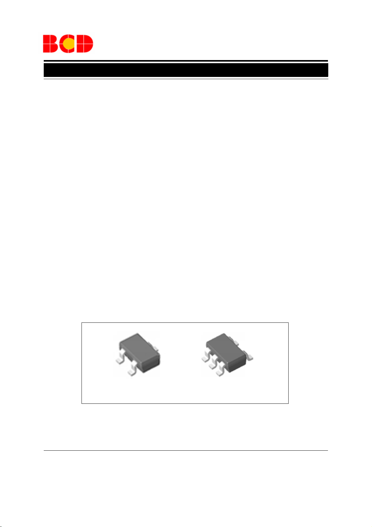
The AP2210 is available in space saving SOT-23-3 and
SOT-23-5 packages.
Features
· Up to 300mA Output Current
· Excellent ESR Stability
· Low Standby Current
· Low Dropout Voltage: V
· High Output Accuracy: ± 1%
· Good Ripple Rejection Ability: 75dB at 100Hz
and I
· Tight Load and Line Regulation
· Low Temperature Coefficient
· Over Current Protection
· Thermal Protection
· Reverse-battery Protection
· Logic-controlled Enable
OUT
=100µA
=250mV at 300mA
DROP
Applications
· Cellular Phones
· Cordless Phones
· Wireless Communicators
· PDAs/Palmtops
· PC Mother Board
· Consumer Electronics
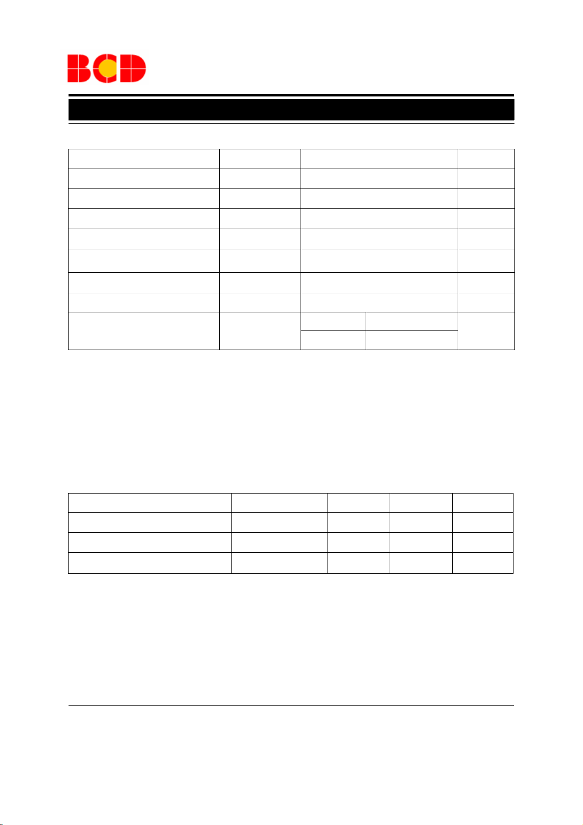
SOT-23-3
Figure 1. Package Types of AP2210
Jan. 2012 Rev. 1. 6 BCD Semiconductor Manufacturing Limited
1
SOT-23-5
Page 2
Data Sheet
300mA RF ULDO REGULATOR AP2210
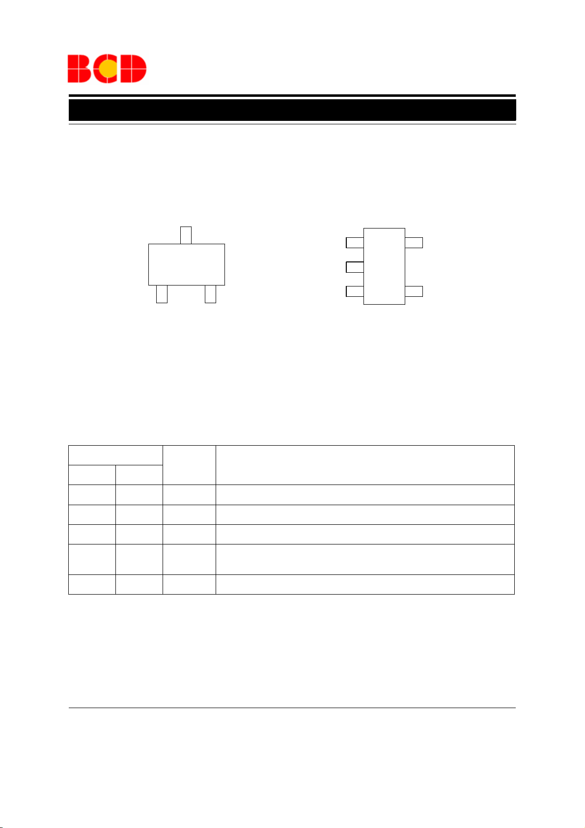
Pin Configuration
(SOT-23-3)
Pin Description
Pin Number
SOT-23-3 SOT-23-5
N Package
VIN
3
21
GND VOUT
Figure 2. Pin Configuration of AP2210 (Top View)
Pin Name
K Package
(SOT-23-5)
VIN
GND
EN
1
2
34
Function
5
VOUT
BYP/ADJ
1 2 GND Ground
2 5 VOUT Regulated output voltage
3 1 VIN Input voltage
3 EN Enable input: CMOS or TTL compatible input. Logic high=enable, logic
low=shutdown
4 BYP/ADJ Bypass capacitor for low noise operation/Adjustable Output
Jan. 2012 Rev. 1. 6 BCD Semiconductor Manufacturing Limited
2
Page 3
Data Sheet
300mA RF ULDO REGULATOR AP2210
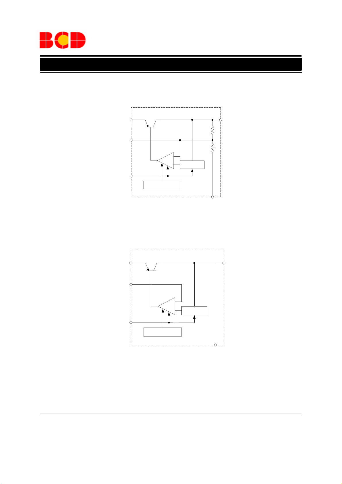
Functional Block Diagram
2 (5)3 (1)
VIN
BYP
EN
(4)
(3)
+
-
Current Limit
Thermal Shutdown
Bandgap
Ref.
1 (2)
VOUT
A (B)
A for SOT-23-3
B for SOT-23-5
GND
Fixed Version
VIN
ADJ
1
4
5
+
Bandgap
Ref.
2
EN
3
-
Current Limit
Thermal Shutdown
GND
ADJ Version (For SOT-23-5)
Figure 3. Functional Block Diagram of AP2210
VOUT
Jan. 2012 Rev. 1. 6 BCD Semiconductor Manufacturing Limited
3
Page 4
Data Sheet
300mA RF ULDO REGULATOR AP2210
Ordering Information
Package
SOT-23-3
Circuit Type
Package
N: SOT-23-3
K: SOT-23-5
Temperature
Range
-40 to 125
o
C
AP2210 -
E1: Lead Free
G1: Green
TR: Tape and Reel
2.5: Fixed Output 2.5V
2.8: Fixed Output 2.8V
3.0: Fixed Output 3.0V
3.3: Fixed Output 3.3V
3.6: Fixed Output 3.6V
4.0: Fixed Output 4.0V
5.0: Fixed Output 5.0V
ADJ: Adjustable Output
Part Number Marking ID
Lead Free Green Lead Free Green
AP2210N-2.5TRE1 AP2210N-2.5TRG1 EH2 GH2 Tape & Reel
AP2210N-2.8TRE1 AP2210N-2.8TRG1 EH3 GH3 Tape & Reel
AP2210N-3.0TRE1 AP2210N-3.0TRG1 EH4 GH4 Tape & Reel
AP2210N-3.3TRE1 AP2210N-3.3TRG1 EH5 GH5 Tape & Reel
AP2210N-3.6TRG1 GB7 Tape & Reel
Packing
Typ e
AP2210N-4.0TRG1 GC7 Tape & Reel
AP2210N-5.0TRG1 GH9 Tape & Reel
AP2210K-2.5TRE1 AP2210K-2.5TRG1 E5C G5C Tape & Reel
AP2210K-2.8TRE1 AP2210K-2.8TRG1 E5F G5F Tape & Reel
AP2210K-3.0TRE1 AP2210K-3.0TRG1 E5H G5H Tape & Reel
AP2210K-3.3TRE1 AP2210K-3.3TRG1 E5K G5K Tape & Reel
SOT-23-5
BCD Semiconductor's Pb-free products, as designated with "E1" suffix in the part number, are RoHS compliant. Products with
"G1" suffix are available in green packages.
-40 to 125
o
C
AP2210K-3.6TRG1 G5I Tape & Reel
AP2210K-4.0TRG1 G5J Tape & Reel
AP2210K-5.0TRG1 G5L Tape & Reel
AP2210K-ADJTRG1 G5M Tape & Reel
Jan. 2012 Rev. 1. 6 BCD Semiconductor Manufacturing Limited
4
Page 5
Data Sheet
300mA RF ULDO REGULATOR AP2210
Absolute Maximum Ratings (Note 1)
Parameter
Supply Input Voltage V
Enable Input Voltage V
Power Dissipation P
Lead Temperature (Soldering, 10sec)
Junction Temperature
Storage Temperature
ESD (Machine Model)
Symbol Value
15 V
15 V
260
150
-65 to 150
300 V
T
LEAD
T
ESD
IN
EN
D
T
STG
Internally Limited (Thermal Protection) W
J
Unit
o
C
o
C
o
C
SOT-23-3 200
Thermal Resistance (No Heatsink) θ
JA
SOT-23-5 200
o
C/W
Note 1: Stresses greater than those listed under "Absolute Maximum Ratings" may cause permanent damage to the device.
These are stress ratings only, and functional operation of the device at these or any other conditions beyond those indicated
under "Recommended Operating Conditions" is not implied. Exposure to "Absolute Maximum Ratings" for extended periods
may affect device reliability.
Recommended Operating Conditions
Parameter Symbol Min Max Unit
Supply Input Voltage V
Enable Input Voltage V
Operating Junction Temperature T
IN
EN
J
Jan. 2012 Rev. 1. 6 BCD Semiconductor Manufacturing Limited
5
2.5 13.2 V
0 13.2 V
-40 125
o
C
Page 6

Data Sheet
300mA RF ULDO REGULATOR AP2210
Electrical Characteristics (Continued)
AP2210-2.5 Electrical Characteristics
VIN=3.5V, I
otherwise specified.
unless
=100µA, CIN=1.0µF, C
OUT
=2.2µF, VEN≥
OUT
2.0V, TJ=25oC,
Bold
typeface applies over -40oC≤TJ≤
125oC (Note 2),
Parameter Symbol Conditions Min Typ Max Unit
Output Voltage Accuracy
Output Voltage
Temperature Coefficient
(Note 3)
Line Regulation
Load Regulation
(Note 4)
∆V
∆V
(∆V
OUT/VOUT
OUT/VOUT
/∆T
OUT
V
RLINE
V
RLOAD
Variation from specified
V
OUT
)/∆T 48
VIN=3.5V to 13.2V
I
=0.1mA to 300mA
OUT
I
=100µA
OUT
-1 1
-2 2
120
1.5 4.5
16
15 50
12
30
%
µV/
ppm/
mV
mV
70
I
OUT
=50mA
110 150
230
Dropout Voltage (Note 5)
V
DROP
I
OUT
=100mA
140 250
mV
300
I
OUT
=150mA
165 275
350
I
OUT
=300mA
250 400
500
Standby Current
Ground Pin Current
(Note 6)
I
STD
I
GND
VEN≤0.4V (shutdown) 0.01 1
V
≤0.18V (shutdown) 5
EN
VEN≥2.0V, I
OUT
=100µA
100 150
180
V
≥2.0V, I
EN
OUT
=50mA
350 600
800
V
≥2.0V, I
EN
OUT
=150mA
1.3 1.9
2.5
V
≥2.0V, I
EN
OUT
=300mA
410
µA
µA
mA
15
Ripple Rejection PSRR f=100Hz, I
V
Current Limit I
Output Noise
LIMIT
e
no
=0V 450 900 mA
OUT
I
=50mA, C
OUT
100pF from BYP to GND
=100µA75dB
OUT
=2.2µF,
OUT
260
o
C
o
C
HznV /
Jan. 2012 Rev. 1. 6 BCD Semiconductor Manufacturing Limited
6
Page 7

Data Sheet
300mA RF ULDO REGULATOR AP2210
Electrical Characteristics (Continued)
AP2210-2.5 Electrical Characteristics
VIN=3.5V, I
unless
otherwise specified.
Parameter Symbol Conditions Min Typ Max Unit
Enable Input Logic-low Voltage
Enable Input Logic-high Voltage V
Enable Input Logic-low Current
Enable Input Logic-high Current
=100µA, CIN=1.0µF, C
OUT
=2.2µF, VEN≥
OUT
V
IL
IH
I
IL
I
IH
2.0V, TJ=25oC,
Regulator shutdown
Bold
typeface applies over -40oC≤TJ≤
125oC (Note 2),
0.4
0.18
Regulator enabled 2.0 V
VIL≤0.4V 0.01 1
V
≤0.18V 2
IL
VIL≥2.0V 5 20
V
≥2.0V 25
IL
µA
µA
V
Note 2: Specifications in bold type are limited to
-40oC≤TJ≤
125oC. Limits over temperature are guaranteed by design, but not
tested in production.
Note 3: Output voltage temperature coefficient is defined as the worst case voltage change divided by the total temperature
range.
Note 4: Regulation is measured at constant junction temperature using low duty cycle pulse testing. Parts are tested for load
regulation in the load range from 0.1mA to 300mA. Changes in output voltage due to heating effects are covered by the thermal
regulation specification.
Note 5: Dropout voltage is defined as the input to output differential at which the output voltage drops 1% (T
o
40
C≤TJ≤
125oC)
below its nominal value measured at 1V differential.
=25oC) or 2% (-
J
Note 6: Ground pin current is the regulator quiescent current plus pass transistor base current. The total current drawn from the
supply is the sum of the load current plus the ground pin current.
Jan. 2012 Rev. 1. 6 BCD Semiconductor Manufacturing Limited
7
Page 8
Data Sheet
300mA RF ULDO REGULATOR AP2210
Electrical Characteristics (Continued)
AP2210-2.8 Electrical Characteristics
VIN=3.8V, I
otherwise specified.
unless
=100µA, CIN=1.0µF, C
OUT
=2.2µF, VEN≥
OUT
2.0V, TJ=25oC,
Bold
typeface applies over -40oC≤TJ≤
125oC (Note 2),
Parameter Symbol Conditions Min Typ Max Unit
Output Voltage Accuracy
Output Voltage
Temperature Coefficient
(Note 3)
Line Regulation
Load Regulation
(Note 4)
∆V
∆V
(∆V
OUT/VOUT
OUT/VOUT
/∆T
OUT
V
RLINE
V
RLOAD
Variation from specified
V
OUT
)/∆T 42.8
VIN=3.8V to 13.2V
I
=0.1mA to 300mA
OUT
I
=100µA
OUT
-1 1
-2 2
120
1.5 4.5
16
15 50
12
30
%
µV/
ppm/
mV
mV
70
I
OUT
=50mA
110 150
230
Dropout Voltage (Note 5)
V
DROP
I
OUT
=100mA
140 250
mV
300
I
OUT
=150mA
165 275
350
I
OUT
=300mA
250 400
500
Standby Current
Ground Pin Current
(Note 6)
I
STD
I
GND
VEN≤0.4V (shutdown) 0.01 1
V
≤0.18V (shutdown) 5
EN
VEN≥2.0V, I
OUT
=100µA
100 150
180
V
≥2.0V, I
EN
OUT
=50mA
350 600
800
V
≥2.0V, I
EN
OUT
=150mA
1.3 1.9
2.5
V
≥2.0V, I
EN
OUT
=300mA
410
µA
µA
mA
15
Ripple Rejection PSRR f=100Hz, I
V
Current Limit I
Output Noise
LIMIT
e
no
=0V 450 900 mA
OUT
I
=50mA, C
OUT
100pF from BYP to GND
=100µA75dB
OUT
=2.2µF,
OUT
260
o
C
o
C
HznV /
Jan. 2012 Rev. 1. 6 BCD Semiconductor Manufacturing Limited
8
Page 9
Data Sheet
300mA RF ULDO REGULATOR AP2210
Electrical Characteristics (Continued)
AP2210-2.8 Electrical Characteristics
VIN=3.8V, I
unless
otherwise specified.
Parameter Symbol Conditions Min Typ Max Unit
Enable Input Logic-low Voltage
Enable Input Logic-high Voltage V
Enable Input Logic-low Current
Enable Input Logic-high Current
=100µA, CIN=1.0µF, C
OUT
=2.2µF, VEN≥
OUT
V
IL
IH
I
IL
I
IH
2.0V, TJ=25oC,
Regulator shutdown
Bold
typeface applies over -40oC≤TJ≤
125oC (Note 2),
0.4
0.18
Regulator enabled 2.0 V
VIL≤0.4V 0.01 1
V
≤0.18V 2
IL
VIL≥2.0V 5 20
V
≥2.0V 25
IL
µA
µA
V
Note 2: Specifications in bold type are limited to
-40oC≤TJ≤
125oC. Limits over temperature are guaranteed by design, but not
tested in production.
Note 3: Output voltage temperature coefficient is defined as the worst case voltage change divided by the total temperature
range.
Note 4: Regulation is measured at constant junction temperature using low duty cycle pulse testing. Parts are tested for load
regulation in the load range from 0.1mA to 300mA. Changes in output voltage due to heating effects are covered by the thermal
regulation specification.
Note 5: Dropout voltage is defined as the input to output differential at which the output voltage drops 1% (T
o
40
C≤TJ≤
125oC)
below its nominal value measured at 1V differential.
=25oC) or 2% (-
J
Note 6: Ground pin current is the regulator quiescent current plus pass transistor base current. The total current drawn from the
supply is the sum of the load current plus the ground pin current.
Jan. 2012 Rev. 1. 6 BCD Semiconductor Manufacturing Limited
9
Page 10
Data Sheet
300mA RF ULDO REGULATOR AP2210
Electrical Characteristics (Continued)
AP2210-3.0 Electrical Characteristics
VIN=4V, I
unless
Parameter Symbol Conditions Min Typ Max Unit
Output Voltage Accuracy
Output Voltage
Temperature Coefficient
(Note 3)
=100µA, CIN=1.0µF, C
OUT
otherwise specified.
∆V
∆V
(∆V
OUT/VOUT
=2.2µF, VEN≥
OUT
OUT/VOUT
/∆T
OUT
2.0V, TJ=25oC,
Variation from specified
V
OUT
Bold
typeface applies over -40oC≤TJ≤
-1 1
-2 2
120
)/∆T 40
125oC (Note 2),
%
µV/
ppm/
o
C
o
C
Line Regulation
Load Regulation
(Note 4)
Dropout Voltage (Note 5)
Standby Current
V
RLINE
V
RLOAD
V
DROP
I
STD
VIN=4V to 13.2V
I
=0.1mA to 300mA
OUT
I
=100µA
OUT
=50mA
I
OUT
I
=100mA
OUT
I
=150mA
OUT
=300mA
I
OUT
VEN≤0.4V (shutdown) 0.01 1
V
≤0.18V (shutdown) 5
EN
VEN≥2.0V, I
≥2.0V, I
V
V
V
EN
≥2.0V, I
EN
≥2.0V, I
EN
Ground Pin Current
(Note 6)
I
GND
Ripple Rejection PSRR f=100Hz, I
V
Current Limit I
Output Noise
LIMIT
e
no
=0V 450 900 mA
OUT
I
=50mA, C
OUT
100pF from BYP to GND
1.5 4.5
12
mV
16
30
mV
15 50
70
110 150
230
140 250
mV
300
165 275
350
250 400
500
µA
OUT
OUT
=100µA
=50mA
100 150
180
350 600
µA
800
OUT
OUT
=150mA
=300mA
1.3 1.9
2.5
410
mA
15
=100µA75dB
OUT
=2.2µF,
OUT
260
HznV /
Jan. 2012 Rev. 1. 6 BCD Semiconductor Manufacturing Limited
10
Page 11

Data Sheet
300mA RF ULDO REGULATOR AP2210
Electrical Characteristics (Continued)
AP2210-3.0 Electrical Characteristics
VIN=4V, I
unless
Parameter Symbol Conditions Min Typ Max Unit
Enable Input Logic-low Voltage
Enable Input Logic-high Voltage V
Enable Input Logic-low Current
Enable Input Logic-high Current
=100µA, CIN=1.0µF, C
OUT
otherwise specified.
=2.2µF, VEN≥
OUT
V
IL
IH
I
IL
I
IH
2.0V, TJ=25oC,
Regulator shutdown
Bold
typeface applies over -40oC≤TJ≤
125oC (Note 2),
0.4
0.18
Regulator enabled 2.0 V
VIL≤0.4V 0.01 1
V
≤0.18V 2
IL
VIL≥2.0V 5 20
V
≥2.0V 25
IL
µA
µA
V
Note 2: Specifications in bold type are limited to
-40oC≤TJ≤
125oC. Limits over temperature are guaranteed by design, but not
tested in production.
Note 3: Output voltage temperature coefficient is defined as the worst case voltage change divided by the total temperature
range.
Note 4: Regulation is measured at constant junction temperature using low duty cycle pulse testing. Parts are tested for load
regulation in the load range from 0.1mA to 300mA. Changes in output voltage due to heating effects are covered by the thermal
regulation specification.
Note 5: Dropout voltage is defined as the input to output differential at which the output voltage drops 1% (T
o
40
C≤TJ≤
125oC)
below its nominal value measured at 1V differential.
=25oC) or 2% (-
J
Note 6: Ground pin current is the regulator quiescent current plus pass transistor base current. The total current drawn from the
supply is the sum of the load current plus the ground pin current.
Jan. 2012 Rev. 1. 6 BCD Semiconductor Manufacturing Limited
11
Page 12

Data Sheet
300mA RF ULDO REGULATOR AP2210
Electrical Characteristics (Continued)
AP2210-3.3 Electrical Characteristics
VIN=4.3V, I
unless
otherwise specified.
Parameter Symbol Conditions Min Typ Max Unit
Output Voltage Accuracy
Output Voltage
Temperature Coefficient
(Note 3)
=100µA, CIN=1.0µF, C
OUT
∆V
∆V
(∆V
OUT/VOUT
=2.2µF, VEN≥
OUT
OUT/VOUT
/∆T
OUT
2.0V, TJ=25oC,
Variation from specified
V
OUT
Bold
typeface applies over -40oC≤TJ≤
-1 1
-2 2
120
)/∆T 36.3
125oC (Note 2),
%
µV/
ppm/
o
C
o
C
Line Regulation
Load Regulation
(Note 4)
Dropout Voltage (Note 5)
Standby Current
V
RLINE
V
RLOAD
V
DROP
I
STD
VIN=4.3V to 13.2V
I
=0.1mA to 300mA
OUT
I
=100µA
OUT
=50mA
I
OUT
I
=100mA
OUT
I
=150mA
OUT
=300mA
I
OUT
VEN≤0.4V (shutdown) 0.01 1
V
≤0.18V (shutdown) 5
EN
VEN≥2.0V, I
≥2.0V, I
V
V
V
EN
≥2.0V, I
EN
≥2.0V, I
EN
Ground Pin Current
(Note 6)
I
GND
Ripple Rejection PSRR f=100Hz, I
V
Current Limit I
Output Noise
LIMIT
e
no
=0V 450 900 mA
OUT
I
=50mA, C
OUT
100pF from BYP to GND
1.5 4.5
12
mV
16
30
mV
15 50
70
110 150
230
140 250
mV
300
165 275
350
250 400
500
µA
OUT
OUT
=100µA
=50mA
100 150
180
350 600
µA
800
OUT
OUT
=150mA
=300mA
1.3 1.9
2.5
410
mA
15
=100µA75dB
OUT
=2.2µF,
OUT
260
HznV /
Jan. 2012 Rev. 1. 6 BCD Semiconductor Manufacturing Limited
12
Page 13

Data Sheet
300mA RF ULDO REGULATOR AP2210
Electrical Characteristics (Continued)
AP2210-3.3 Electrical Characteristics
VIN=4.3V, I
unless
otherwise specified.
Parameter Symbol Conditions Min Typ Max Unit
Enable Input Logic-low Voltage
Enable Input Logic-high Voltage V
Enable Input Logic-low Current
Enable Input Logic-high Current
Note 2: Specifications in bold type are limited to
tested in production.
Note 3: Output voltage temperature coefficient is defined as the worst case voltage change divided by the total temperature
range.
Note 4: Regulation is measured at constant junction temperature using low duty cycle pulse testing. Parts are tested for load
regulation in the load range from 0.1mA to 300mA. Changes in output voltage due to heating effects are covered by the thermal
regulation specification.
Note 5: Dropout voltage is defined as the input to output differential at which the output voltage drops 1% (T
o
40
C≤TJ≤
Note 6: Ground pin current is the regulator quiescent current plus pass transistor base current. The total current drawn from the
supply is the sum of the load current plus the ground pin current.
=100µA, CIN=1.0µF, C
OUT
=2.2µF, VEN≥
OUT
V
IL
IH
I
IL
I
IH
-40oC≤TJ≤
125oC)
below its nominal value measured at 1V differential.
2.0V, TJ=25oC,
Regulator shutdown
Bold
typeface applies over -40oC≤TJ≤
125oC (Note 2),
0.4
0.18
Regulator enabled 2.0 V
VIL≤0.4V 0.01 1
V
≤0.18V 2
IL
VIL≥2.0V 5 20
V
≥2.0V 25
IL
µA
µA
125oC. Limits over temperature are guaranteed by design, but not
=25oC) or 2% (-
J
V
Jan. 2012 Rev. 1. 6 BCD Semiconductor Manufacturing Limited
13
Page 14

Data Sheet
300mA RF ULDO REGULATOR AP2210
Electrical Characteristics (Continued)
AP2210-3.6 Electrical Characteristics
VIN=4.6V, I
otherwise specified.
unless
=100µA, CIN=1.0µF, C
OUT
=2.2µF, VEN≥
OUT
2.0V, TJ=25oC,
Bold
typeface applies over -40oC≤TJ≤
125oC (Note 2),
Parameter Symbol Conditions Min Typ Max Unit
Output Voltage Accuracy
Output Voltage
Temperature Coefficient
(Note 3)
Line Regulation
Load Regulation
(Note 4)
∆V
∆V
(∆V
OUT/VOUT
OUT/VOUT
/∆T
OUT
V
RLINE
V
RLOAD
Variation from specified
V
OUT
)/∆T 48
VIN=4.6V to 13.2V
I
=0.1mA to 300mA
OUT
I
=100µA
OUT
-1 1
-2 2
120
1.5 4.5
16
15 50
12
30
%
µV/
ppm/
mV
mV
70
I
OUT
=50mA
110 150
230
Dropout Voltage (Note 5)
V
DROP
I
OUT
=100mA
140 250
mV
300
I
OUT
=150mA
165 275
350
I
OUT
=300mA
250 400
500
Standby Current
Ground Pin Current
(Note 6)
I
STD
I
GND
VEN≤0.4V (shutdown) 0.01 1
V
≤0.18V (shutdown) 5
EN
VEN≥2.0V, I
OUT
=100µA
100 150
180
V
≥2.0V, I
EN
OUT
=50mA
350 600
800
V
≥2.0V, I
EN
OUT
=150mA
1.3 1.9
2.5
V
≥2.0V, I
EN
OUT
=300mA
410
µA
µA
mA
15
Ripple Rejection PSRR f=100Hz, I
V
Current Limit I
Output Noise
LIMIT
e
no
=0V 450 900 mA
OUT
I
=50mA, C
OUT
100pF from BYP to GND
=100µA75dB
OUT
=2.2µF,
OUT
260
o
C
o
C
HznV /
Jan. 2012 Rev. 1. 6 BCD Semiconductor Manufacturing Limited
14
Page 15

Data Sheet
300mA RF ULDO REGULATOR AP2210
Electrical Characteristics (Continued)
AP2210-3.6 Electrical Characteristics
VIN=4.6V, I
unless
otherwise specified.
Parameter Symbol Conditions Min Typ Max Unit
Enable Input Logic-low Voltage
Enable Input Logic-high Voltage V
Enable Input Logic-low Current
Enable Input Logic-high Current
=100µA, CIN=1.0µF, C
OUT
=2.2µF, VEN≥
OUT
V
IL
IH
I
IL
I
IH
2.0V, TJ=25oC,
Regulator shutdown
Bold
typeface applies over -40oC≤TJ≤
125oC (Note 2),
0.4
0.18
Regulator enabled 2.0 V
VIL≤0.4V 0.01 1
V
≤0.18V 2
IL
VIL≥2.0V 5 20
V
≥2.0V 25
IL
µA
µA
V
Note 2: Specifications in bold type are limited to
-40oC≤TJ≤
125oC. Limits over temperature are guaranteed by design, but not
tested in production.
Note 3: Output voltage temperature coefficient is defined as the worst case voltage change divided by the total temperature
range.
Note 4: Regulation is measured at constant junction temperature using low duty cycle pulse testing. Parts are tested for load
regulation in the load range from 0.1mA to 300mA. Changes in output voltage due to heating effects are covered by the thermal
regulation specification.
Note 5: Dropout voltage is defined as the input to output differential at which the output voltage drops 1% (T
o
40
C≤TJ≤
125oC)
below its nominal value measured at 1V differential.
=25oC) or 2% (-
J
Note 6: Ground pin current is the regulator quiescent current plus pass transistor base current. The total current drawn from the
supply is the sum of the load current plus the ground pin current.
Jan. 2012 Rev. 1. 6 BCD Semiconductor Manufacturing Limited
15
Page 16

Data Sheet
300mA RF ULDO REGULATOR AP2210
Electrical Characteristics (Continued)
AP2210-4.0 Electrical Characteristics
VIN=5.0V, I
otherwise specified.
unless
=100µA, CIN=1.0µF, C
OUT
=2.2µF, VEN≥
OUT
2.0V, TJ=25oC,
Bold
typeface applies over -40oC≤TJ≤
125oC (Note 2),
Parameter Symbol Conditions Min Typ Max Unit
Output Voltage Accuracy
Output Voltage
Temperature Coefficient
(Note 3)
Line Regulation
Load Regulation
(Note 4)
∆V
∆V
(∆V
OUT/VOUT
OUT/VOUT
/∆T
OUT
V
RLINE
V
RLOAD
Variation from specified
V
OUT
)/∆T 48
VIN=5.0V to 13.2V
I
=0.1mA to 300mA
OUT
I
=100µA
OUT
-1 1
-2 2
120
1.5 4.5
16
15 50
12
30
%
µV/
ppm/
mV
mV
70
I
OUT
=50mA
110 150
230
Dropout Voltage (Note 5)
V
DROP
I
OUT
=100mA
140 250
mV
300
I
OUT
=150mA
165 275
350
I
OUT
=300mA
250 400
500
Standby Current
Ground Pin Current
(Note 6)
I
STD
I
GND
VEN≤0.4V (shutdown) 0.01 1
V
≤0.18V (shutdown) 5
EN
VEN≥2.0V, I
OUT
=100µA
100 150
180
V
≥2.0V, I
EN
OUT
=50mA
350 600
800
V
≥2.0V, I
EN
OUT
=150mA
1.3 1.9
2.5
V
≥2.0V, I
EN
OUT
=300mA
410
µA
µA
mA
15
Ripple Rejection PSRR f=100Hz, I
V
Current Limit I
Output Noise
LIMIT
e
no
=0V 450 900 mA
OUT
I
=50mA, C
OUT
100pF from BYP to GND
=100µA75dB
OUT
=2.2µF,
OUT
260
o
C
o
C
HznV /
Jan. 2012 Rev. 1. 6 BCD Semiconductor Manufacturing Limited
16
Page 17

Data Sheet
300mA RF ULDO REGULATOR AP2210
Electrical Characteristics (Continued)
AP2210-4.0 Electrical Characteristics
VIN=5.0V, I
unless
otherwise specified.
Parameter Symbol Conditions Min Typ Max Unit
Enable Input Logic-low Voltage
Enable Input Logic-high Voltage V
Enable Input Logic-low Current
Enable Input Logic-high Current
=100µA, CIN=1.0µF, C
OUT
=2.2µF, VEN≥
OUT
V
IL
IH
I
IL
I
IH
2.0V, TJ=25oC,
Regulator shutdown
Bold
typeface applies over -40oC≤TJ≤
125oC (Note 2),
0.4
0.18
Regulator enabled 2.0 V
VIL≤0.4V 0.01 1
V
≤0.18V 2
IL
VIL≥2.0V 5 20
V
≥2.0V 25
IL
µA
µA
V
Note 2: Specifications in bold type are limited to
-40oC≤TJ≤
125oC. Limits over temperature are guaranteed by design, but not
tested in production.
Note 3: Output voltage temperature coefficient is defined as the worst case voltage change divided by the total temperature
range.
Note 4: Regulation is measured at constant junction temperature using low duty cycle pulse testing. Parts are tested for load
regulation in the load range from 0.1mA to 300mA. Changes in output voltage due to heating effects are covered by the thermal
regulation specification.
Note 5: Dropout voltage is defined as the input to output differential at which the output voltage drops 1% (T
o
40
C≤TJ≤
125oC)
below its nominal value measured at 1V differential.
=25oC) or 2% (-
J
Note 6: Ground pin current is the regulator quiescent current plus pass transistor base current. The total current drawn from the
supply is the sum of the load current plus the ground pin current.
Jan. 2012 Rev. 1. 6 BCD Semiconductor Manufacturing Limited
17
Page 18

Data Sheet
300mA RF ULDO REGULATOR AP2210
Electrical Characteristics (Continued)
AP2210-5.0 Electrical Characteristics
VIN=6.0V, I
otherwise specified.
unless
=100µA, CIN=1.0µF, C
OUT
=2.2µF, VEN≥
OUT
2.0V, TJ=25oC,
Bold
typeface applies over -40oC≤TJ≤
125oC (Note 2),
Parameter Symbol Conditions Min Typ Max Unit
Output Voltage Accuracy
Output Voltage
Temperature Coefficient
(Note 3)
Line Regulation
Load Regulation
(Note 4)
∆V
∆V
(∆V
OUT/VOUT
OUT/VOUT
/∆T
OUT
V
RLINE
V
RLOAD
Variation from specified
V
OUT
)/∆T 48
VIN=6.0V to 13.2V
I
=0.1mA to 300mA
OUT
I
=100µA
OUT
-1 1
-2 2
120
1.5 4.5
16
15 50
12
30
%
µV/
ppm/
mV
mV
70
I
OUT
=50mA
110 150
230
Dropout Voltage (Note 5)
V
DROP
I
OUT
=100mA
140 250
mV
300
I
OUT
=150mA
165 275
350
I
OUT
=300mA
250 400
500
Standby Current
Ground Pin Current
(Note 6)
I
STD
I
GND
VEN≤0.4V (shutdown) 0.01 1
V
≤0.18V (shutdown) 5
EN
VEN≥2.0V, I
OUT
=100µA
100 150
180
V
≥2.0V, I
EN
OUT
=50mA
350 600
800
V
≥2.0V, I
EN
OUT
=150mA
1.3 1.9
2.5
V
≥2.0V, I
EN
OUT
=300mA
410
µA
µA
mA
15
Ripple Rejection PSRR f=100Hz, I
V
Current Limit I
Output Noise
LIMIT
e
no
=0V 450 900 mA
OUT
I
=50mA, C
OUT
100pF from BYP to GND
=100µA75dB
OUT
=2.2µF,
OUT
260
o
C
o
C
HznV /
Jan. 2012 Rev. 1. 6 BCD Semiconductor Manufacturing Limited
18
Page 19

Data Sheet
300mA RF ULDO REGULATOR AP2210
Electrical Characteristics (Continued)
AP2210-5.0 Electrical Characteristics
VIN=6.0V, I
unless
otherwise specified.
Parameter Symbol Conditions Min Typ Max Unit
Enable Input Logic-low Voltage
Enable Input Logic-high Voltage V
Enable Input Logic-low Current
Enable Input Logic-high Current
=100µA, CIN=1.0µF, C
OUT
=2.2µF, VEN≥
OUT
V
IL
IH
I
IL
I
IH
2.0V, TJ=25oC,
Regulator shutdown
Bold
typeface applies over -40oC≤TJ≤
125oC (Note 2),
0.4
0.18
Regulator enabled 2.0 V
VIL≤0.4V 0.01 1
V
≤0.18V 2
IL
VIL≥2.0V 5 20
V
≥2.0V 25
IL
µA
µA
V
Note 2: Specifications in bold type are limited to
-40oC≤TJ≤
125oC. Limits over temperature are guaranteed by design, but not
tested in production.
Note 3: Output voltage temperature coefficient is defined as the worst case voltage change divided by the total temperature
range.
Note 4: Regulation is measured at constant junction temperature using low duty cycle pulse testing. Parts are tested for load
regulation in the load range from 0.1mA to 300mA. Changes in output voltage due to heating effects are covered by the thermal
regulation specification.
Note 5: Dropout voltage is defined as the input to output differential at which the output voltage drops 1% (T
o
40
C≤TJ≤
125oC)
below its nominal value measured at 1V differential.
=25oC) or 2% (-
J
Note 6: Ground pin current is the regulator quiescent current plus pass transistor base current. The total current drawn from the
supply is the sum of the load current plus the ground pin current.
Jan. 2012 Rev. 1. 6 BCD Semiconductor Manufacturing Limited
19
Page 20

Data Sheet
300mA RF ULDO REGULATOR AP2210
Electrical Characteristics (Continued)
AP2210-ADJ Electrical Characteristics
VIN=V
(Note 2), unless
OUT
+1V, I
=100µA, CIN=1.0µF, C
OUT
otherwise specified.
=2.2µF, VEN≥
OUT
2.0V, TJ=25oC,
Bold
typeface applies over -40oC≤TJ≤
125oC
Parameter Symbol Conditions Min Typ Max Unit
Output Voltage Accuracy
Output Voltage
Temperature Coefficient
(Note 3)
Line Regulation
Load Regulation
(Note 4)
Standby Current
Ground Pin Current
(Note 6)
∆V
∆V
(∆V
OUT/VOUT
OUT/VOUT
/∆T
OUT
V
RLINE
V
RLOAD
I
STD
I
GND
Variation from specified
V
OUT
)/∆T 48
VIN=
V
+1V
OUT
I
=0.1mA to 300mA
OUT
to 13.2V
VEN≤0.4V (shutdown) 0.01 1
≤0.18V (shutdown) 5
V
EN
VEN≥2.0V, I
V
≥2.0V, I
EN
VEN≥2.0V, I
≥2.0V, I
V
EN
OUT
OUT
OUT
OUT
=100µA
=50mA
=150mA
=300mA
-1 1
-2 2
120
1.5 4.5
16
100 150
180
350 600
800
1.3 1.9
410
12
30
2.5
%
µV/
ppm/
mV
mV
µA
µA
mA
15
Ripple Rejection PSRR f=100Hz, I
Current Limit I
Output Noise
LIMIT
e
no
V
=0V 450 900 mA
OUT
I
=50mA, C
OUT
100pF from BYP to GND
=100µA75dB
OUT
=2.2µF,
OUT
260
o
C
o
C
HznV /
Enable Input Logic-low
Vo l t a g e
Enable Input Logic-high
Vo l t a g e
Enable Input Logic-low
Current
Enable Input Logic-high
Current
V
IL
V
IH
I
IL
I
IH
Regulator shutdown
Regulator enabled 2.0 V
VIL≤0.4V 0.01 1
≤0.18V 2
V
IL
VIL≥2.0V 5 20
≥2.0V 25
V
IL
0.4
0.18
V
µA
µA
Jan. 2012 Rev. 1. 6 BCD Semiconductor Manufacturing Limited
20
Page 21

Data Sheet
300mA RF ULDO REGULATOR AP2210
Electrical Characteristics (Continued)
AP2210-ADJ Electrical Characteristics
VIN=V
(Note 2), unless
Note 2: Specifications in bold type are limited to
tested in production.
Note 3: Output voltage temperature coefficient is defined as the worst case voltage change divided by the total temperature
range.
Note 4: Regulation is measured at constant junction temperature using low duty cycle pulse testing. Parts are tested for load
regulation in the load range from 0.1mA to 300mA. Changes in output voltage due to heating effects are covered by the thermal
regulation specification.
Note 6: Ground pin current is the regulator quiescent current plus pass transistor base current. The total current drawn from the
supply is the sum of the load current plus the ground pin current.
OUT
+1V, I
=100µA, CIN=1.0µF, C
OUT
otherwise specified.
=2.2µF, VEN≥
OUT
-40oC≤TJ≤
2.0V, TJ=25oC,
125oC. Limits over temperature are guaranteed by design, but not
Bold
typeface applies over -40oC≤TJ≤
125oC
Jan. 2012 Rev. 1. 6 BCD Semiconductor Manufacturing Limited
21
Page 22

Data Sheet
300mA RF ULDO REGULATOR AP2210
Typical Performance Characteristics
3.0150
3.0125
3.0100
3.0075
3.0050
3.0025
3.0000
2.9975
2.9950
Output Voltage (V)
2.9925
2.9900
2.9875
2.9850
-50 -25 0 25 50 75 100 125
AP2210-3.0
VIN=4V, I
OUT
CIN=1.0µF, C
=10mA
=2.2µF
OUT
Junction Temperature (oC)
Figure 4. Output Voltage vs. Junction Temperature
5.0
4.5
4.0
3.5
3.0
2.5
2.0
1.5
Ground Pin Current (mA)
1.0
0.5
0.0
0 50 100 150 200 250 300
TA=25oC
CIN=1.0µF, C
Output Current (mA)
OUT
=2.2µF
550
500
450
400
350
300
250
200
Dropout Voltage (mv)
150
100
50
I
=50mA
OUT
I
=100mA
OUT
I
=150mA
OUT
I
=300mA
OUT
0
-60 -40 -20 0 20 40 60 80 100 120 140
CIN=1.0µF, C
OUT
=2.2µF
Junction Temperature (oC)
Figure 5. Dropout Voltage vs. Junction Temperature
5.0
4.5
4.0
3.5
3.0
2.5
2.0
1.5
Ground Pin Current (mA)
1.0
0.5
0.0
-60 -40 -20 0 20 40 60 80 100 120 140
Junction Temperature (oC)
AP2210-3.0
VIN=4V,CIN=1.0µF,C
I
=50mA
OUT
I
=100mA
OUT
I
=150mA
OUT
I
=300mA
OUT
OUT
=2.2µF
Figure 6. Ground Pin Current vs. Output Current Figure 7. Ground Pin Current vs. Junction Temperature
Jan. 2012 Rev. 1. 6 BCD Semiconductor Manufacturing Limited
22
Page 23

Data Sheet
300mA RF ULDO REGULATOR AP2210
Typical Performance Characteristics (Continued)
20
AP2210-3.0
18
V
=4V, CIN=1.0µF
IN
16
C
=2.2µF, I
OUT
14
12
10
8
Enable Current (µA)
6
4
2
0
-50 -25 0 25 50 75 100 125
=100µA
OUT
Junction Temperature (oC)
VEN=1.8V
VEN=2.0V
VEN=3.0V
VEN=3.7V
2.0
1.8
1.6
1.4
1.2
1.0
Enable Voltage (V)
0.8
0.6
0.4
-50 -25 0 25 50 75 100 125
VEN=logic high
VEN=logic low
Junction Temperature (oC)
AP2210-3.0
CIN=1.0µF, C
VIN=4V, I
OUT
=2.2µF
OUT
=100µA
Figure 8. Enable Current vs. Junction Temperature Figure 9. Enable Voltage vs. Junction Temperature
10
1
V/ Hz
µ
0.1
5.5
5
AP2210-3.0
4.5
(0.5V/Div)
IN
4
V
0.01
AP2210-3.0
V
Output Noise ( )
0.001
0.0001
=4.5V, I
IN
C
=1.0µF, C
IN
C
BYP
10 100 1k 10k 100k 1M 10M
=100pF
OUT
=10mA
OUT
=2.2µF
Frequency (Hz)
Figure 10. Output Noise vs. Frequency
50
0
(50mV/Div)
-50
OUT
V
∆
-100
(Conditions: V
Time (20µs/Div)
Figure 11. Line Transient
=4 to 5V, VEN=2V, I
IN
C
=2.2µF)
OUT
OUT
=1mA,
Jan. 2012 Rev. 1. 6 BCD Semiconductor Manufacturing Limited
23
Page 24

Data Sheet
300mA RF ULDO REGULATOR AP2210
Typical Performance Characteristics (Continued)
600
400
200
(200mA/Div)
OUT
I
0
AP2210-3.0
50
0
(50mV/Div)
OUT
-50
V
∆
-100
Time (20µs/Div)
Figure 12. Load Transient
(Conditions: VIN=4V, VEN=2V,
=1.0
C
100
90
80
70
60
50
40
PSRR (dB)
30
20
10
0
10 100 1k 10k 100k 1M
IN
Frequency (Hz)
µF,
C
OUT
AP2210-3.0
VIN=4V, V
I
OUT
I
=10mA to 300mA,
OUT
=2.2µF)
RIPPLE
=10mA, C
=1V
OUT
PP
=2.2µF
6
4
2
(2V/Div)
EN
0
V
AP2210-3.0
2
0
(2V/Div)
OUT
-2
V
-4
Time (40µs/Div)
Figure 13. VEN vs. V
(Conditions: VEN=0 to 2V, VIN=4V, I
=1.0
C
0.9
0.8
0.7
0.6
0.5
0.4
0.3
Power Dissipation (W)
0.2
0.1
0.0
25 50 75 100 125 150
µF,
IN
Ambient Temperature (oC)
C
OUT
OUT
OUT
=30mA,
=2.2µF)
AP2210-3.0
SOT-23-3 Package
No Heatsink
Figure 14. PSRR vs. Frequency
Figure 15. Power Dissipation vs. Ambient Temperature
Jan. 2012 Rev. 1. 6 BCD Semiconductor Manufacturing Limited
24
Page 25

Data Sheet
300mA RF ULDO REGULATOR AP2210
Typical Performance Characteristics (Continued)
0.9
0.8
0.7
0.6
0.5
0.4
0.3
Power Dissipation (W)
0.2
0.1
0.0
25 50 7 5 100 125 150
AP2210-3.0
SOT-23-5 Package
No Heatsink
Ambient Temperature (oC)
Figure 16. Power Dissipation vs. Ambient Temperature
1000
100
C
OUT
No Bypass Capacitor
=2.2µF
1000
C
=1µF
OUT
100
10
ESR (Ω)
1
0.1
0.01
50 100 150 200 250 300
Stable Area
No Bypass Capacitor
Output Current (mA)
Figure 17. ESR vs. Output Current
1000
100
C
OUT
No Bypass Capacitor
=4.7µF
10
ESR (Ω)
1
0.1
0.01
50 100 150 200 25 0 300
Stable Area
Output Current (mA)
Figure 18. ESR vs. Output Current
10
ESR (Ω)
1
0.1
0.01
50 100 150 200 250 300
Stable Area
Output Current (mA)
Figure 19. ESR vs. Output Current
Jan. 2012 Rev. 1. 6 BCD Semiconductor Manufacturing Limited
25
Page 26

Data Sheet
300mA RF ULDO REGULATOR AP2210
Typical Application
V
V
IN
IN
VIN=4.0V
VIN=4.0V
C
IN
1.0 µ F
C
1.0 µ F
AP2210-3.0
VIN
IN
VOUT
GND
23
V
OUT
C
OUT
2.2 µ F
=3.0V
V
OUT
1
AP2210-3.0
1
VIN
2
GND
3
EN
VOUT
BYP
5
4
C
BYP
V
=3.0V
OUT
V
OUT
C
OUT
2.2 µF
100pF
For Fixed Version
Jan. 2012 Rev. 1. 6 BCD Semiconductor Manufacturing Limited
26
Page 27

Data Sheet
300mA RF ULDO REGULATOR AP2210
Typical Application (Continued)
V
IN
C
IN
V
=1.25V*(1+R2/R1)
OUT
AP2210-ADJ
ADJ
5
R1
4
R2
1
VIN
2
GND
V
EN
3
EN
VOUT
For Adjustable Version
Figure 20. Typical Application of AP2210 (Note 7)
V
OUT
C
OUT
Note 7: Dropout voltage is 250mV when TA=25oC. In order to obtain a normal output voltage, V
+0.25V is the minimum
OUT
input voltage which will results a low PSRR, imposing a bad influence on system. Therefore, the recommended input voltage
+1V to 13.2V. For AP2210-3.0 version, its input voltage can be set from 4V(V
is V
OUT
+1V) to 13.2V.
OUT
Jan. 2012 Rev. 1. 6 BCD Semiconductor Manufacturing Limited
27
Page 28

Data Sheet
300mA RF ULDO REGULATOR AP2210
Application Information
Input Capacitor
A 1
µF minimum capacitor is recommended to be
placed between V
and GND.
IN
Output Capacitor
It is required to prevent oscillation. 1.0
is recommended when C
mum is recommended when C
is unused. 2.2µF mini-
BYP
BYP
µF minimum
is 100pF. The out-
put capacitor may be increased to improve transient
response.
Noise Bypass Capacitor
Bypass capacitor is connected to the internal voltage
reference. A small capacitor connected from BYP to
GND make this reference quiet, resulting in a
significant reduction in output noise, but the ESR
stable area will be narrowed. In order to keep the
output stability, it is recommended to use the bypass
capacitor no more than 100pF.
The start-up speed of the AP2210 is inversely
proportional to the value of reference bypass
capacitor. In some cases, if output noise is not a
major concern and rapid turn-on is necessary, omit
C
and leave BYP open.
BYP
Power Dissipation
Thermal shutdown may take place if exceeding the
maximum power dissipation in application. Under all
possible operating conditions, the junction tempera-
ture must be within the range specified under absolute maximum ratings to avoid thermal shutdown.
To determine if the power dissipated in the regulator
reaches the maximum power dissipation (see figure
16, 17), using:
T
= PD*θJA + T
J
PD=(VIN-V
Where: T
ings for the junction temperature; V
A
)*I
OUT
J≤TJ(max)
OUT+VIN*IGND
, T
is absolute maximum rat-
J(max)
IN*IGND
can be
ignored due to its small value.
T
J(max)
is 150
o
C, θ
is 200
JA
o
C/W, no heatsink is
required since the package alone will dissipate
enough heat to satisfy these requirements unless the
calculated value for power dissipation exceeds the
limit.
Example (3.0V version):
I
=300mA, TA=50oC, V
OUT
o
C-50oC)/(0.3A*200oC/W)+3.0V=4.67V
(150
IN(Max)
is:
Therefore, for good performance, please make sure
that input voltage is less than 4.67V without heatsink
when T
=50oC.
A
Jan. 2012 Rev. 1. 6 BCD Semiconductor Manufacturing Limited
28
Page 29

Data Sheet
300mA RF ULDO REGULATOR AP2210
Mechanical Dimensions
SOT-23-3 Unit: mm(inch)
2.820(0.111)
3.020(0.119)
0.300(0.012)
0.600(0.024)
0.100(0.004)
0.200(0.008)
2.650(0.104)
2.950(0.116)
0.950(0.037)
TYP
MAX.
1.450(0.057)
1.800(0.071)
2.000(0.079)
1.500(0.059)
0.300(0.012)
0.500(0.020)
0.900(0.035)
1.300(0.051)
0.200(0.008)
1.700(0.067)
0.000(0.000)
0.150(0.006)
0
°
8
°
Jan. 2012 Rev. 1. 6 BCD Semiconductor Manufacturing Limited
29
Page 30

Data Sheet
300mA RF ULDO REGULATOR AP2210
Mechanical Dimensions (Continued)
SOT-23-5 Unit: mm(inch)
2.820(0.111)
3.020(0.119)
)
)
4
2
2
1
0
0
.
.
0
)
)
9
)
)
6
4
1
0
1
1
.
.
0
0
(
(
0
0
5
5
6
9
.
.
2
2
7
5
6
0
0
.
.
0
0
(
(
0
0
0
0
5
7
.
.
1
1
0.200(0.008)
0
(
(
0
0
0
0
3
6
.
.
0
0
0.100(0.004)
0.200(0.008)
0.950(0.037)
P
Y
T
)
7
5
0
.
X
0
A
(
0
M
5
4
.
1
1.800(0.071)
2.000(0.079)
0.300(0.012)
0.400(0.016)
0
0
0
0
0
9
.
.
1
0
0
3
0
0
7
.
0
R
0
(
0
0
0
.
0
(
0
5
1
.
5
3
0
(
0
.
)
1
5
0
.
0
(
)
8
2
0
.
0
(
F
E
0°
8°
)
0
0
0
.
)
6
0
0
.
)
Jan. 2012 Rev. 1. 6 BCD Semiconductor Manufacturing Limited
30
Page 31

BCD Semiconductor Manufacturing Limited
IMPORTANT NOTICE
IMPORTANT NOTICE
BCD Semiconductor Manufacturing Limited reserves the right to make changes without further notice to any products or specifi-
BCD Semiconductor Manufacturing Limited reserves the right to make changes without further notice to any products or specifi-
cations herein. BCD Semiconductor Manufacturing Limited does not assume any responsibility for use of any its products for any
cations herein. BCD Semiconductor Manufacturing Limited does not assume any responsibility for use of any its products for any
particular purpose, nor does BCD Semiconductor Manufacturing Limited assume any liability arising out of the application or use
particular purpose, nor does BCD Semiconductor Manufacturing Limited assume any liability arising out of the application or use
of any its products or circuits. BCD Semiconductor Manufacturing Limited does not convey any license under its patent rights or
of any its products or circuits. BCD Semiconductor Manufacturing Limited does not convey any license under its patent rights or
other rights nor the rights of others.
other rights nor the rights of others.
http://www.bcdsemi.com
MAIN SITE
MAIN SITE
- Headquarters
BCD Semiconductor Manufacturing Limited
BCD Semiconductor Manufactur ing Limited
- Wafer Fab
No. 1600, Zi Xing Road, Shanghai ZiZhu Science-based Industrial Park, 200241, China
Shanghai SIM-BCD Semiconductor Manufacturing Limited
Tel: +86-21-24162266, Fax: +86-21-24162277
800, Yi Shan Road, Shanghai 200233, China
Tel: +86-21-6485 1491, Fax: +86-21-5450 0008
REGIONAL SALES OFFICE
Shenzhen Office
REGIONAL SALES OFFICE
Shanghai SIM-BCD Semiconductor Manufacturing Co., Ltd., Shenzhen Office
Shenzhen Office
Unit A Room 1203, Skyworth Bldg., Gaoxin Ave.1.S., Nanshan District, Shenzhen,
Shanghai SIM-BCD Semiconductor Manufacturing Co., Ltd. Shenzhen Office
China
Advanced Analog Circuits (Shanghai) Corporation Shenzhen Office
Tel: +86-755-8826 7951
Room E, 5F, Noble Center, No.1006, 3rd Fuzhong Road, Futian District, Shenzhen 518026, China
Fax: +86-755-8826 7865
Tel: +86-755-8826 7951
Fax: +86-755-8826 7865
- Wafer Fab
BCD Semiconductor Manufacturing Limited
Shanghai SIM-BCD Semiconductor Manufacturing Co., Ltd.
- IC Design Group
800 Yi Shan Road, Shanghai 200233, China
Advanced Analog Circuits (Shanghai) Corporation
Tel: +86-21-6485 1491, Fax: +86-21-5450 0008
8F, Zone B, 900, Yi Shan Road, Shanghai 200233, China
Tel: +86-21-6495 9539, Fax: +86-21-6485 9673
Taiwan Office
BCD Semiconductor (Taiwan) Company Limited
Taiwan Office
4F, 298-1, Rui Guang Road, Nei-Hu District, Taipei,
BCD Semiconductor (Taiwan) Company Limited
Tai wan
4F, 298-1, Rui Guang Road, Nei-Hu District, Taipei,
Tel: +886-2-2656 2808
Taiwan
Fax: +886-2-2656 2806
Tel: +886-2-2656 2808
Fax: +886-2-2656 2806
USA Office
BCD Semiconductor Corp.
USA Office
30920 Huntwood Ave. Hayward,
BCD Semiconductor Corporation
CA 94544, USA
30920 Huntwood Ave. Hayward,
Tel : +1-510-324-2988
CA 94544, U.S.A
Fax: +1-510-324-2788
Tel : +1-510-324-2988
Fax: +1-510-324-2788
 Loading...