

Page 1
Data Sheet
WIDE INPUT VOLTAGE RANGE, 150mA ULDO REGULATOR AP2204
General Description
The AP2204 series is a positive voltage regulator IC
fabricated by high voltage EPNP process.
The AP2204 has features of wide input voltage range,
high accurcay, high ripple rejection, low dropout
voltage, low noise, current limit and ultra-low
quiescent current which make it ideal for use in various
USB and portable devices.
The IC consists of a voltage reference, an error
amplifier, a resistor network for setting output voltage,
a current limit circuit for current protection, and a chip
enable circuit.
The AP2204 has 1.5V, 1.8V, 2.5V, 2.8V, 3.0V, 3.3V,
5.0V fixed voltage versions and adjustable voltage
version.
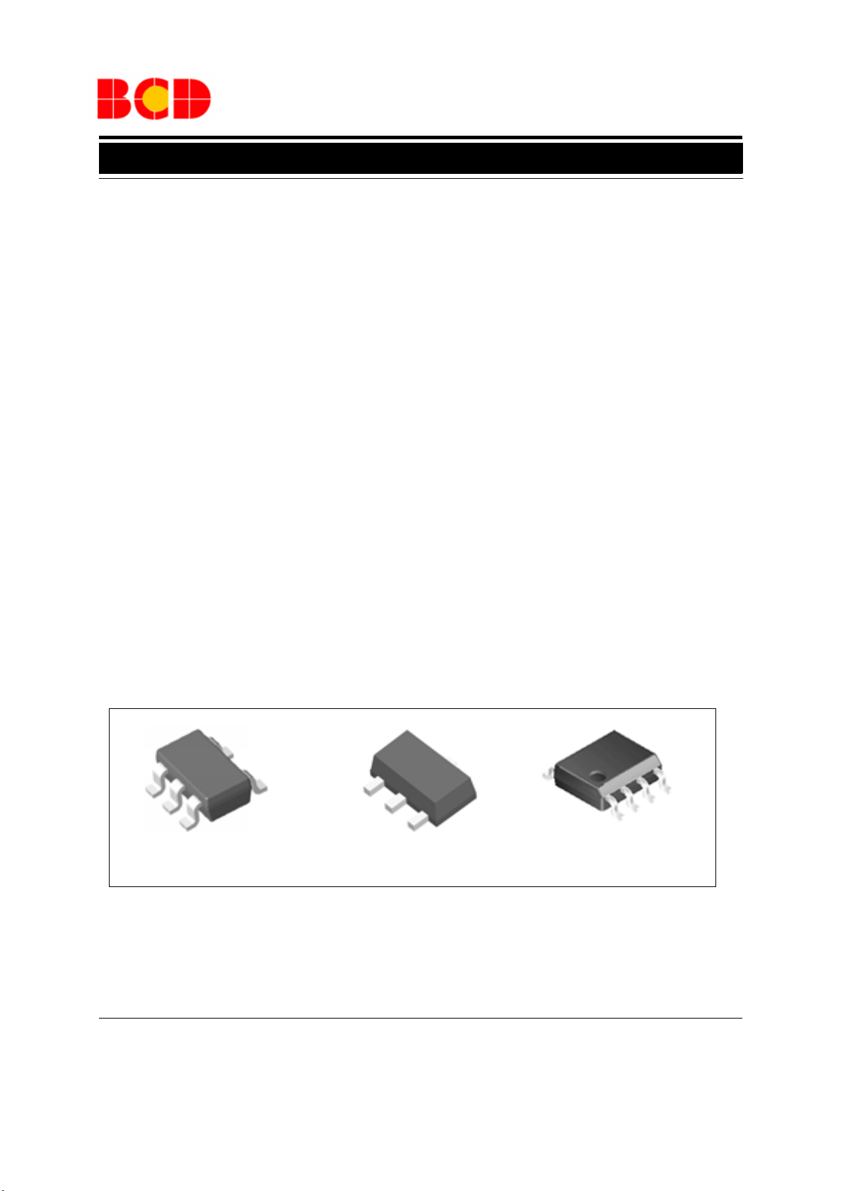
The AP2204 is available in space-saving SOT-23-5,
SOT-89 and PSOP-8 packages.
Features
· Wide Input Voltage Range: 2.3V to 24V
· Wide Output Voltage Range: 1.24V to 22V
· Excellent Ripple Rejection: 60dB@ f=1kHz
· Low Dropout Voltage: V
I
· Low Ground Current
· High Output Voltage Accuracy
· Compatible with Low ESR Ceramic Capacitor
· Excellent Line/Load Regulation
· Thermal Shutdown Function
OUT
=100µA
DROP
=100mV@
Applications
· Battery-powered Equipment
· Laptop, Palmtops, Notebook Computers
· Portable Information Appliances
SOT-23-5
Figure 1. Package Types of AP2204
Jul 2011 Rev. 2. 2 BCD Semiconductor Manufacturing Limited
SOT-89 PSOP-8
1
Page 2
Data Sheet
WIDE INPUT VOLTAGE RANGE, 150mA ULDO REGULATOR AP2204
Pin Configuration
R Package
(SOT-89)
R (Note 1) RA (Note 2)
VOUT
3
2
GND
GND
1
VIN
K Package
(SOT-23-5)
VIN
GND
1
2
EN
34
Note 1: The substrate/exposed pad should be connected to GND or open.
Note 2: The substrate/exposed pad should be connected to VIN or open.
Note 3: The exposed pad should be connected to GND for better dissipation.
Figure 2. Pin Configuration of AP2204 (Top View)
5
VOUT
ADJ/NC
ADJ/NC
VIN
VOUT
NC
NC
MP Package
(PSOP-8)
1
Exposed
2
3
4
Pad
(Note 3)
VOUT
3
VIN
2
GND
1
VIN
8
GND
7
6
NC
5
EN
Pin Description
Pin Number
SOT-23-5 PSOP-8
SOT-89
RRA
1 8 1 2 VIN Input voltage
2 7 2 1 GND Ground
3 5 EN Enable input
4 4 ADJ/NC Adjust output for ADJ version/No connected for fixed version
5 1 3 3 VOUT Regulated output voltage
Jul 2011 Rev. 2. 2 BCD Semiconductor Manufacturing Limited
Pin Name Function
2
Page 3
Data Sheet
WIDE INPUT VOLTAGE RANGE, 150mA ULDO REGULATOR AP2204
Functional Block Diagram
1 (1) {2} [8]
VIN VOUT
3 [5]
EN
ENABLE
1.24V
-
+
VREF
+
-
OTP
5 (3) {3} [1]
2 (2) {1} [7]
GND
Fixed Output Voltage
VIN
EN
1 (8)
3 (5)
ENABLE
5 (1)
VOUT
A (B) {C} [D]
A for SOT-23-5
B for SOT-89 (R)
C for SOT-89 (RA)
D for PSOP-8
1.24V
-
+
VREF
+
-
OTP
4 (4)
ADJ
A (B)
2 (7)
GND
A for SOT-23-5
B for PSOP-8
Adjustable Output Voltage
Figure 3. Functional Block Diagram of AP2204
Jul 2011 Rev. 2. 2 BCD Semiconductor Manufacturing Limited
3
Page 4
Data Sheet
WIDE INPUT VOLTAGE RANGE, 150mA ULDO REGULATOR AP2204
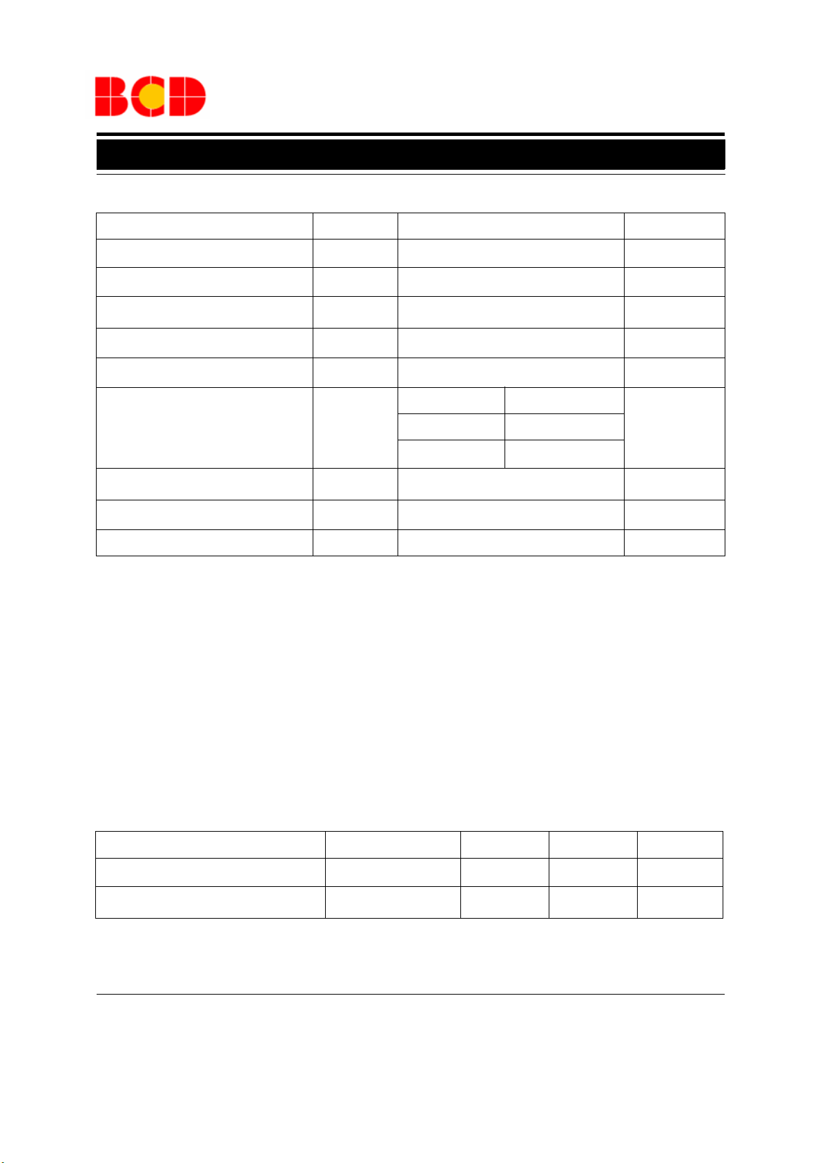
Ordering Information
Ordering Information
Package
Circuit Type
Package
K: SOT-23-5
R/RA: SOT-89
MP: PSOP-8
Temperature
Range
AP2204 -
G1: Green
TR: Tape and Reel
ADJ: Adjustable Output
1.
5: Fixed
Output
1.5V
1.8: Fixed Output 1.8V
2.5: Fixed Output 2.5V
2.8: Fixed Output 2.8V
3.0: Fixed Output 3.0V
3.3: Fixed Output 3.3V
5.0: Fixed Output 5.0V
Output Voltage
ADJ AP2204K-ADJTRG1 GAF Tape & Reel
1.5V AP2204K-1.5TRG1 GBH Tape & Reel
1.8V AP2204K-1.8TRG1 GAG
Part Number Marking ID
Green Green
Packing Type
Tap e & Reel
Tap e & Reel
Tap e & Reel
Tap e & Reel
Tap e & Reel
Tap e & Reel
Tap e & Reel
Tap e & Reel
Tap e & Reel
SOT-23-5
SOT-89
-40 to 85
-40 to 85
o
C
o
C
2.5V AP2204K-2.5TRG1 GAD
2.8V AP2204K-2.8TRG1 GAE
3.0V AP2204K-3.0TRG1 GEF Tape & Reel
3.3V AP2204K-3.3TRG1 GAH Tape & Reel
5.0V AP2204K-5.0TRG1 GAI
1.5V (R) AP2204R-1.5TRG1 G22C
1.8V (R) AP2204R-1.8TRG1 G31C
2.5V (R) AP2204R-2.5TRG1 G22D Tape & Reel
2.8V (R) AP2204R-2.8TRG1 G22E
3.0V (R) AP2204R-3.0TRG1 G22F
3.3V (R) AP2204R-3.3TRG1 G31D Tape & Reel
5.0V (R) AP2204R-5.0TRG1 G31E
Jul 2011 Rev. 2. 2 BCD Semiconductor Manufacturing Limited
4
Page 5
Data Sheet
WIDE INPUT VOLTAGE RANGE, 150mA ULDO REGULATOR AP2204
Ordering Information (Continued)
Package
SOT-89
PSOP-8
Temperature
Range
-40 to 85
-40 to 85
o
C
o
C
Output Voltage
1.5V (RA) AP2204RA-1.5TRG1 G22O
1.8V (RA) AP2204RA-1.8TRG1 G27O
2.5V (RA) AP2204RA-2.5TRG1 G28O Tape & Reel
2.8V (RA) AP2204RA-2.8TRG1 G31O
3.0V (RA) AP2204RA-3.0TRG1 G33O
3.3V (RA) AP2204RA-3.3TRG1 G37O Tape & Reel
5.0V (RA) AP2204RA-5.0TRG1 G41O
ADJ AP2204MP-ADJTRG1 2204MP-ADJG1 Tape & Reel
1.5V AP2204MP-1.5TRG1 2204MP-1.5G1 Tape & Reel
1.8V AP2204MP-1.8TRG1 2204MP-1.8G1
2.5V AP2204MP-2.5TRG1 2204MP-2.5G1
2.8V AP2204MP-2.8TRG1 2204MP-2.8G1
3.0V AP2204MP-3.0TRG1 2204MP-3.0G1 Tape & Reel
3.3V AP2204MP-3.3TRG1 2204MP-3.3G1 Tape & Reel
Part Number Marking ID
Packing Type
Green Green
Tap e & R e el
Tap e & R e el
Tap e & R e el
Tap e & R e el
Tap e & R e el
Tap e & R e el
Tap e & R e el
Tap e & R e el
5.0V AP2204MP-5.0TRG1 2204MP-5.0G1
BCD Semiconductor's products, as designated with "G1" suffix in the part number, are RoHS compliant and Green.
Jul 2011 Rev. 2. 2
BCD Semiconductor Manufacturing Limited
Tap e & R e el
5
Page 6
Data Sheet
WIDE INPUT VOLTAGE RANGE, 150mA ULDO REGULATOR AP2204
Absolute Maximum Ratings (Note 4)
Parameter
Supply Input Voltage V
Enable Input Voltage V
Output Current I
Lead Temperature (Soldering, 10sec)
Operating Junction Temperature
Symbol Value
38 V
38 V
250 mA
260
150
T
IN
CE
OUT
LEAD
T
J
Unit
o
C
o
C
SOT-23-5 250
Thermal Resistance θ
Storage Temperature Range T
ESD (Machine Model)
ESD (Human Body Model)
JA
STG
SOT-89 165
PSOP-8 (Note 5)
-65 to 150
275
2000
51
o
C/W
o
C
V
V
Note 4: Stresses greater than those listed under "Absolute Maximum Ratings" may cause permanent damage to the device.
These are stress ratings only, and functional operation of the device at these or any other conditions beyond those indicated
under "Recommended Operating Conditions" is not implied. Exposure to "Absolute Maximum Ratings" for extended periods
may affect device reliability.
Note 5: θ
is measured with the component mounted on a 2-Layer FR-4 PCB board with 1.5cm*1.5cm thermal sink pad in free
JA
air.
Recommended Operating Conditions
Parameter Symbol Min Max Unit
Supply Input Voltage V
Operating Junction Temperature T
IN
J
Jul 2011 Rev. 2. 2 BCD Semiconductor Manufacturing Limited
6
2.3 24 V
-40 125
o
C
Page 7

Data Sheet
WIDE INPUT VOLTAGE RANGE, 150mA ULDO REGULATOR AP2204
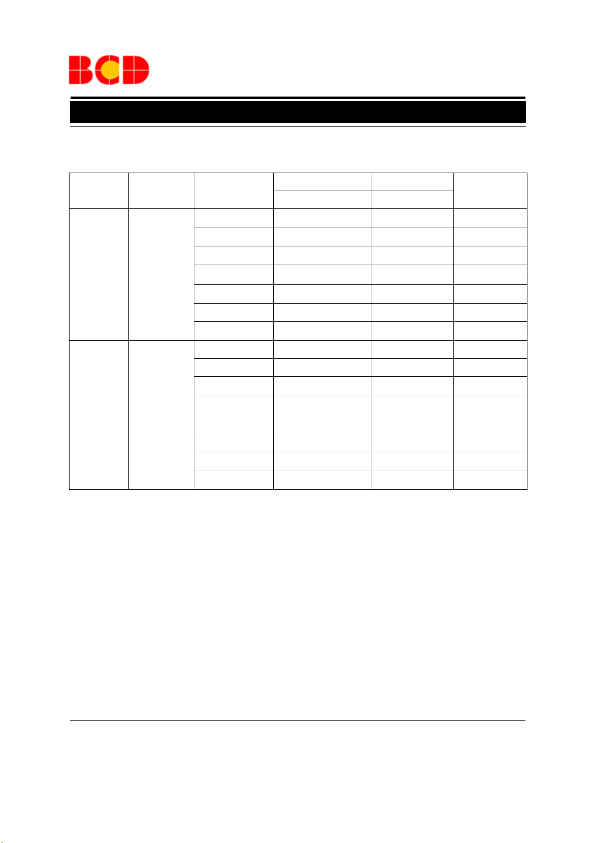
Electrical Characteristics
VIN=V
wise specified.
Parameter Symbol Conditions Min Typ Max Unit
Output Voltage
+1V, TJ=25oC, I
OUT
=100µA, CIN=1.0µF, C
OUT
V
OUT
OUT
=2.2µF,
Bold
typeface applies over -40oC≤TJ≤
Variation from Specified
V
OUT
V
OUT
×98%
125oC, unless
V
OUT
×102%
other-
V
Reference Voltage
V
Input Voltage V
Maximum Output
Current
Line Regulation
Load Regulation ∆V
Dropout Voltage
Ground Current
I
OUT(max)
∆V
OUT
OUT/VOUT
V
I
Standby Current
Power Supply
Rejection Ration
PSRR
REF
IN
DROP
GND
I
STD
/∆V
1.215 1.24 1.265
V
24 V
VIN-V
V
OUT
IN
V
OUT
1mA≤I
I
OUT
I
OUT
I
OUT
I
OUT
I
OUT
I
OUT
I
OUT
I
OUT
VIN=V
V
EN
Ripple 0.5V
VIN=V
=1V
OUT
=98% ×V
OUT
+1V≤VIN≤24V
≤150mA 0.5 %
OUT
150 200 mA
0.05 %
=100µA 100 150
=50mA 270 350
mV
=100mA 320 460
=150mA 360 500
=100µA50µA
=50mA 0.5
=100mA 1.3
mA
=150mA 2.5
+1V
OUT
in OFF Mode
P-P
+1V
OUT
f=100Hz 60
f=1kHz 60
0.01 1.0 µA
dB
Output Voltage
∆V
Temperature
OUT
/(V
Coefficient
RMS Output Noise
ADJ Pin Current I
EN Pin Current I
V
OUT
NOI
ADJ
EN
×∆T)
=100µA,
I
OUT
o
C≤TJ≤125oC
-40
TJ=25oC, 10Hz≤f≤100kHz
I
=100µA
OUT
VEN=V
OUT
+1V
EN“High” Vo l ta ge E N I n pu t Vo lt a ge “High”
EN “Low” Vol t ag e EN In p u t Vo lt a g e “Low”
SOT-23-5 43
Thermal Resistance
(Junction to Case)
θ
JC
PSOP-8 22
Jul 2011 Rev. 2. 2
7
±100
30
0.5
1
2.0
0.4
ppm/
µV
µA
µA
V
V
o
C/WSOT-89 27
rms
o
C
BCD Semiconductor Manufacturing Limited
Page 8

Data Sheet
WIDE INPUT VOLTAGE RANGE, 150mA ULDO REGULATOR AP2204
Typical Performance Characteristics
5.10
5.08
AP2204-5.0
V
5.06
5.04
5.02
5.00
4.98
4.96
Output Voltage (V)
4.94
4.92
4.90
=6V
IN
T
=25oC
J
0 15 30 45 60 75 90 105 120 135 150
Output Current (mA)
Figure 4. Output Voltage vs. Output Current
6.0
5.5
5.0
4.5
4.0
3.5
3.0
2.5
2.0
Output Voltage (V)
1.5
1.0
0.5
0.0
0 50 100 150 200 250 300 350 400 450 500
AP2204-5.0
V
=6V
IN
TJ=-40oC
TJ=25oC
TJ=125oC
Output Current (mA)
Figure 5. Output Voltage vs. Output Current
6.0
5.5
5.0
4.5
4.0
3.5
3.0
2.5
2.0
Output Voltage (V)
1.5
1.0
0.5
0.0
0 50 100 1 50 200 250 300 350 400 450 500
AP2204-5.0
=25oC
T
J
VIN=6V
VIN=12V
VIN=24V
Output Current (mA)
Figure 6. Output Voltage vs. Output Current
600
550
500
450
400
350
300
250
200
Dropout Voltage (mV)
150
100
50
0
0 15 30 45 60 75 90 105 120 135 150
AP2204-5.0
TJ=-40oC
TJ=25oC
TJ=125oC
Output Current (mA)
Figure 7. Dropout Voltage vs. Output Current
Jul 2011 Rev. 2. 2 BCD Semiconductor Manufacturing Limited
8
Page 9

Data Sheet
WIDE INPUT VOLTAGE RANGE, 150mA ULDO REGULATOR AP2204
Typical Performance Characteristics (Continued)
0.60
0.55
AP2204-5.0
Dropout Voltage (V)
0.50
0.45
0.40
0.35
0.30
0.25
0.20
0.15
0.10
0.05
0.00
I
=10mA
OUT
I
=100mA
OUT
I
=150mA
OUT
-40 -20 0 20 40 60 80 100 120
Junction Temperature (oC)
Figure 8. Dropout Voltage vs. Junction Temperature
6.0
5.5
5.0
4.5
4.0
3.5
3.0
2.5
2.0
Output Voltage (V)
1.5
1.0
0.5
0.0
0 2 4 6 8 1012141618202224
Input Voltage (V)
AP2204-5.0
=150mA
I
OUT
TJ=-40oC
TJ=25oC
TJ=125oC
6.0
5.5
5.0
4.5
4.0
3.5
3.0
2.5
2.0
Output Voltage (V)
1.5
1.0
0.5
0.0
0 2 4 6 8 1012141618202224
AP2204-5.0
No Load
TJ=-40oC
TJ=25oC
TJ=125oC
Input Voltage (V)
Figure 9. Output Voltage vs. Input Voltage
5.20
5.16
AP2204-5.0
I
5.12
5.08
5.04
5.00
4.96
4.92
Output Voltage (V)
4.88
4.84
4.80
-40 -20 0 20 40 60 80 100 120
=10mA
OUT
I
=100mA
OUT
I
=150mA
OUT
Junction Temperature (oC)
Figure 10. Output Voltage vs. Input Voltage Figure 11. Output Voltage vs. Junction Temperature
Jul 2011 Rev. 2. 2
BCD Semiconductor Manufacturing Limited
9
Page 10

Data Sheet
WIDE INPUT VOLTAGE RANGE, 150mA ULDO REGULATOR AP2204
Typical Performance Characteristics (Continued)
60
55
50
45
40
35
30
25
20
Supply Current (µA)
15
10
5
0
0 2 4 6 8 1012141618202224
AP2204-5.0
No Load
TJ=-40oC
TJ=25oC
TJ=125oC
Input Voltage (V)
Figure 12. Supply Current vs. Input Voltage
5.0
4.5
AP2204-5.0
4.0
V
=6V
IN
3.5
3.0
2.5
2.0
1.5
Ground Current (mA)
1.0
0.5
0.0
0 153045607590105120135150
TJ=-40oC
TJ=25oC
TJ=125oC
Output Current (mA)
50
48
46
44
42
40
38
36
34
32
30
28
Ground Current (µA)
26
24
22
20
-40 -20 0 20 40 60 80 100 120
AP2204-5.0
V
=6V
IN
No Load
Junction Temperature (oC)
Figure 13. Ground Current vs. Junction Temperature
2.0
1.8
1.6
1.4
1.2
1.0
0.8
0.6
Enable Current (µA)
0.4
0.2
0.0
0 2 4 6 8 10 12 14 16 18 20 22 24
Enable Input Voltage (V)
AP2204-5.0
No Load
=25oC
T
J
Figure 14. Ground Current vs. Output Current
Figure 15. Enable Current vs. Enable Input Voltage
Jul 2011 Rev. 2. 2 BCD Semiconductor Manufacturing Limited
10
Page 11

Data Sheet
WIDE INPUT VOLTAGE RANGE, 150mA ULDO REGULATOR AP2204
Typical Performance Characteristics (Continued)
∆
V
IN
2V/div
∆V
OUT
200mV/div
∆V
IN
5V/div
∆V
OUT
200mV/div
(Conditions: VIN=
∆V
OUT
50mV/div
I
OUT
20mA/div
Figure 16. Line Transient
VEN=3.5V to 8V,
C
=2.2µF, I
OUT
Figure 18. Load Transient
(Conditions: VIN=5V,
I
=1mA to 50mA)
OUT
CIN=1.0µF,
=1mA)
OUT
CIN=1.0µF, C
OUT
=2.2
µF
∆V
OUT
200mV/div
I
OUT
100mA/div
(Conditions: VIN=5V,
Figure 17. Line Transient
(Conditions: VIN=
C
OUT
Figure 19. Load Transient
VEN=5V to 15V,
=2.2µF, I
OUT
CIN=1.0µF, C
I
=1mA to 150mA)
OUT
=1mA)
CIN=1.0µF,
=2.2
OUT
µF
Jul 2011 Rev. 2. 2
BCD Semiconductor Manufacturing Limited
11
Page 12

Data Sheet
WIDE INPUT VOLTAGE RANGE, 150mA ULDO REGULATOR AP2204
Typical Performance Characteristics (Continued)
∆V
∆V
1V/div
∆V
OUT
1V/div
EN
1V/div
∆V
OUT
1V/div
IN
100
90
80
70
60
50
40
PSRR (dB)
30
20
10
0
Figure 20. Enable Input Response
AP2204-3.3
VIN=5V
VIN=20V
100 1k 10k 100k
Frequency (Hz)
Figure 21. Start-up Response
10
9
8
7
6
5
4
AP2204MP-ADJTRG1
3
VIN=12V, V
Output Voltage (V)
2
1
0
0 100 200 300 400 500
OUT
TC=-40oC
TC=25oC
TC=85oC
=7.6V
Output Current (mA)
Figure 22. PSRR vs. Frequency
(Conditions: V
PP
=2V, I
OUT
=10mA)
Figure 23. Output Voltage vs. Output Current
Jul 2011 Rev. 2. 2 BCD Semiconductor Manufacturing Limited
12
Page 13

Data Sheet
WIDE INPUT VOLTAGE RANGE, 150mA ULDO REGULATOR AP2204
Typical Performance Characteristics (Continued)
480
460
440
420
400
380
360
AP2204MP-ADJTRG1
340
V
=7.6V
OUT
VIN=11V
VIN=12V
VIN=13V
-60 -40 -20 0 20 40 60 80 100 120 140
Case Temperature (oC)
Maximum Output Current (mA)
320
300
280
Figure 24. Maximum Output Current vs. Case Temperature
80
AP2204MP-ADJTRG1
V
70
C)
60
o
50
40
Case Temperature (
30
20
=7.6V
OUT
VIN=12V
TA=25oC
2-Layer FR-4 PCB board with
1.5cm*1.5cm thermal sink pad
0 25 50 75 100 125 150 175 200
Output Current (mA)
Figure 25. Case Temperature vs. Output Current
Jul 2011 Rev. 2. 2
BCD Semiconductor Manufacturing Limited
13
Page 14

Data Sheet
WIDE INPUT VOLTAGE RANGE, 150mA ULDO REGULATOR AP2204
Typical Application
AP2204
Fixed Version
V
IN
VIN
VOUT
V
OUT
SOT-89
C
C
IN
1.0µF
GND
OUT
2.2µF
AP2204
Fixed Version
V
IN
VIN
VOUT
V
OUT
SOT-23-5/PSOP-8
1.0µF
V
IN
1.0µF
C
C
IN
EN
GND
NC
OUT
2.2µF
AP2204
ADJ Version
C
OUT
2.2µF
V
OUT
VIN
SOT-23-5/PSOP-8
C
IN
EN ADJ
GND
VOUT
R1
R2
V
OUT=VREF
Figure 26. Typical Application of AP2204
(1+(R1/R2))
Jul 2011 Rev. 2. 2 BCD Semiconductor Manufacturing Limited
14
Page 15

Data Sheet
WIDE INPUT VOLTAGE RANGE, 150mA ULDO REGULATOR AP2204
Mechanical Dimensions
SOT-23-5 Unit: mm(inch)
2.820(0.111)
3.020(0.119)
)
)
2
4
2
1
0
0
.
.
0
)
)
9
)
)
6
4
1
0
1
1
.
.
0
0
(
(
0
0
5
5
6
9
.
.
2
2
7
5
6
0
0
.
.
0
0
(
(
0
0
0
0
5
7
.
.
1
1
0.200(0.008)
0
(
(
0
0
0
0
3
6
.
.
0
0
0.100(0.004)
0.200(0.008)
0.950(0.037)
P
Y
T
)
7
5
0
.
X
0
A
(
0
M
5
4
.
1
1.800(0.071)
2.000(0.079)
0.300(0.012)
0.400(0.016)
0
0
0
0
0
9
.
.
1
0
0
3
0
0
7
.
0
R
0
(
0
0
0
.
0
(
0
5
1
.
5
3
0
(
0
.
)
)
1
5
0
.
0
(
)
8
2
0
.
0
(
F
E
0°
8°
)
0
0
0
.
)
6
0
0
.
Jul 2011 Rev. 2. 2
BCD Semiconductor Manufacturing Limited
15
Page 16

Data Sheet
WIDE INPUT VOLTAGE RANGE, 150mA ULDO REGULATOR AP2204
Mechanical Dimensions (Continued)
SOT-89 Unit: mm(inch)
4.400(0.173)
1.550(0.061)REF
4.600(0.181)
45
1.030(0.041)REF
1.400(0.055)
1.600(0.063)
3.950(0.156)
4.250(0.167)
0.900(0.035)
1.100(0.043)
R0.150(0.006)
0.320(0.013)
0.520(0.020)
3.000(0.118)
TYP
2.300(0.091)
2.600(0.102)
0.320(0.013)
0.520(0.020)
0.480(0.019)
3
2.210(0.087)REF
10
3
1.500(0.059)
1.800(0.071)
2.060(0.081)REF
10
0.350(0.014)
0.450(0.018)
0.320(0.013)REF
1.620(0.064)REF
Jul 2011 Rev. 2. 2 BCD Semiconductor Manufacturing Limited
16
Page 17

Data Sheet
WIDE INPUT VOLTAGE RANGE, 150mA ULDO REGULATOR AP2204
Mechanical Dimensions (Continued)
PSOP-8 Unit: mm(inch)
3.800(0.150)
4.000(0.157)
2.313(0.091)
2.513(0.099)
1.270(0.050)
3.202(0.126)
°
0
°
8
0.170(0.007)
0.250(0.010)
3.402(0.134)
0.330(0.013)
0.510(0.020)
5.800(0.228)
6.200(0.244)
0.400(0.016)
1.270(0.050)
TYP
0.050(0.002)
0.150(0.006)
Note: Eject hole, oriented hole and mold mark is optional.
4.700(0.185)
5.100(0.201)
1.350(0.053)
1.550(0.061)
1.350(0.053)
1.750(0.069)
Jul 2011 Rev. 2. 2
BCD Semiconductor Manufacturing Limited
17
Page 18

BCD Semiconductor Manufacturing Limited
IMPORTANT NOTICE
IMPORTANT NOTICE
BCD Semiconductor Manufacturing Limited reserves the right to make changes without further notice to any products or specifi-
BCD Semiconductor Manufacturing Limited reserves the right to make changes without further notice to any products or specifi-
cations herein. BCD Semiconductor Manufacturing Limited does not assume any responsibility for use of any its products for any
cations herein. BCD Semiconductor Manufacturing Limited does not assume any responsibility for use of any its products for any
particular purpose, nor does BCD Semiconductor Manufacturing Limited assume any liability arising out of the application or use
particular purpose, nor does BCD Semiconductor Manufacturing Limited assume any liability arising out of the application or use
of any its products or circuits. BCD Semiconductor Manufacturing Limited does not convey any license under its patent rights or
of any its products or circuits. BCD Semiconductor Manufacturing Limited does not convey any license under its patent rights or
other rights nor the rights of others.
other rights nor the rights of others.
http://www.bcdsemi.com
MAIN SITE
MAIN SITE
- Headquarters
BCD Semiconductor Manufacturing Limited
BCD Semiconductor Manufactur ing Limited
- Wafer Fab
No. 1600, Zi Xing Road, Shanghai ZiZhu Science-based Industrial Park, 200241, China
Shanghai SIM-BCD Semiconductor Manufacturing Limited
Tel: +86-21-24162266, Fax: +86-21-24162277
800, Yi Shan Road, Shanghai 200233, China
Tel: +86-21-6485 1491, Fax: +86-21-5450 0008
REGIONAL SALES OFFICE
Shenzhen Office
REGIONAL SALES OFFICE
Shanghai SIM-BCD Semiconductor Manufacturing Co., Ltd., Shenzhen Office
Shenzhen Office
Unit A Room 1203, Skyworth Bldg., Gaoxin Ave.1.S., Nanshan District, Shenzhen,
Shanghai SIM-BCD Semiconductor Manufacturing Co., Ltd. Shenzhen Office
China
Advanced Analog Circuits (Shanghai) Corporation Shenzhen Office
Tel: +86-755-8826 7951
Room E, 5F, Noble Center, No.1006, 3rd Fuzhong Road, Futian District, Shenzhen 518026, China
Fax: +86-755-8826 7865
Tel: +86-755-8826 7951
Fax: +86-755-8826 7865
- Wafer Fab
BCD Semiconductor Manufacturing Limited
Shanghai SIM-BCD Semiconductor Manufacturing Co., Ltd.
- IC Design Group
800 Yi Shan Road, Shanghai 200233, China
Advanced Analog Circuits (Shanghai) Corporation
Tel: +86-21-6485 1491, Fax: +86-21-5450 0008
8F, Zone B, 900, Yi Shan Road, Shanghai 200233, China
Tel: +86-21-6495 9539, Fax: +86-21-6485 9673
Taiwan Office
BCD Semiconductor (Taiwan) Company Limited
Taiwan Office
4F, 298-1, Rui Guang Road, Nei-Hu District, Taipei,
BCD Semiconductor (Taiwan) Company Limited
Tai wan
4F, 298-1, Rui Guang Road, Nei-Hu District, Taipei,
Tel: +886-2-2656 2808
Taiwan
Fax: +886-2-2656 2806
Tel: +886-2-2656 2808
Fax: +886-2-2656 2806
USA Office
BCD Semiconductor Corp.
USA Office
30920 Huntwood Ave. Hayward,
BCD Semiconductor Corporation
CA 94544, USA
30920 Huntwood Ave. Hayward,
Tel : +1-510-324-2988
CA 94544, U.S.A
Fax: +1-510-324-2788
Tel : +1-510-324-2988
Fax: +1-510-324-2788
 Loading...