Diodes AP2008 User Manual

AP2008
PWM BUCK CONTROLLER
Features
• PWM Buck Control Circuitry
• Operating voltage can be up to 20V
• Under voltage Lockout (UVLO) Protection
• Short Circuit Protection (SCP)
• Soft-start circuit
• Variable Oscillator Frequency -- 300Khz Max
• 0.77V voltage reference Output
• 8-pin SOP package
• SOP-8L: Available in “Green” Molding Compound
(No Br, Sb)
• Lead Free Finish/ RoHS Compliant (Note 1)
Applications
• Backlight inverter
• LCD Monitor
• XDROM, XDSL Product
• DC/DC converters in computers, etc.
Ordering Information
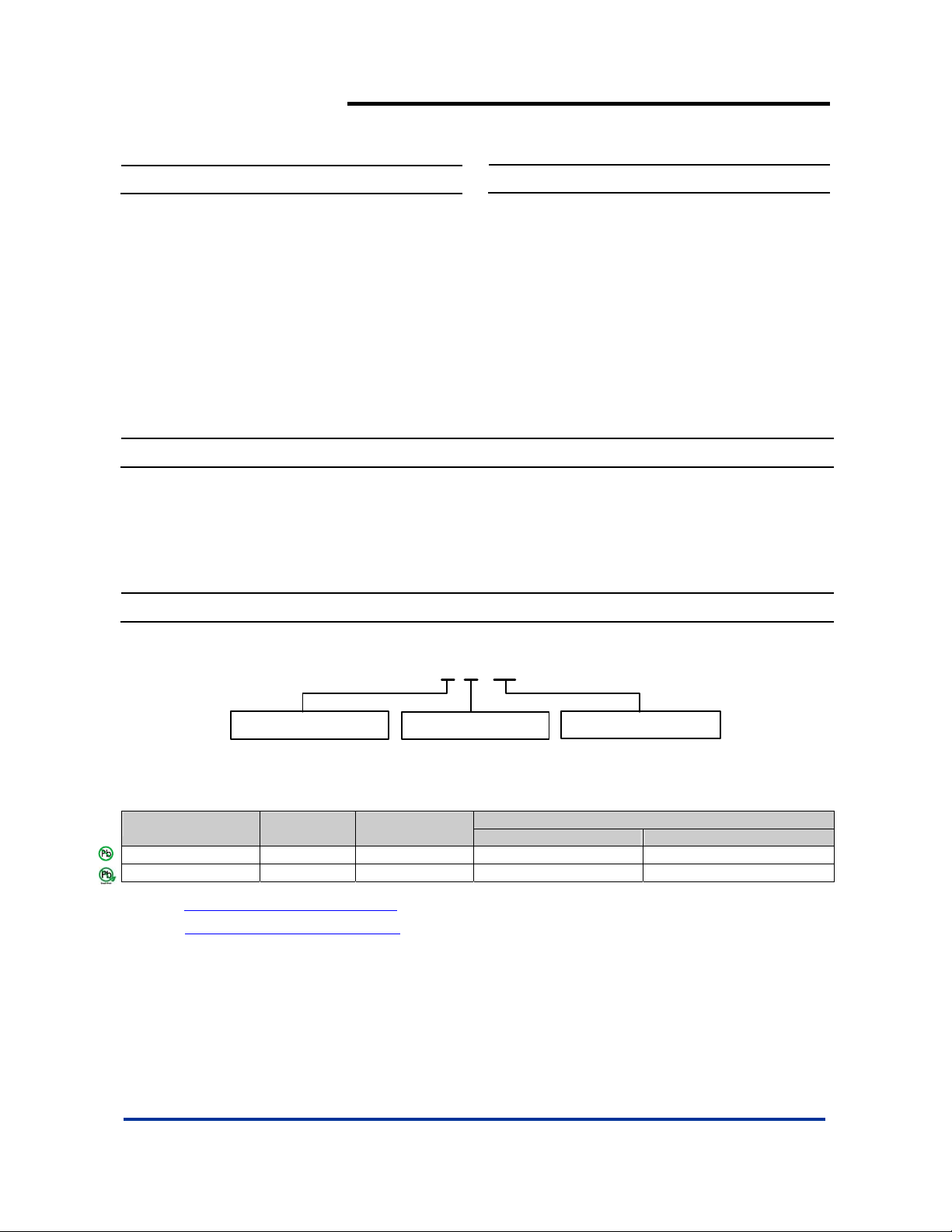
AP 2008 S X - 13
General Description
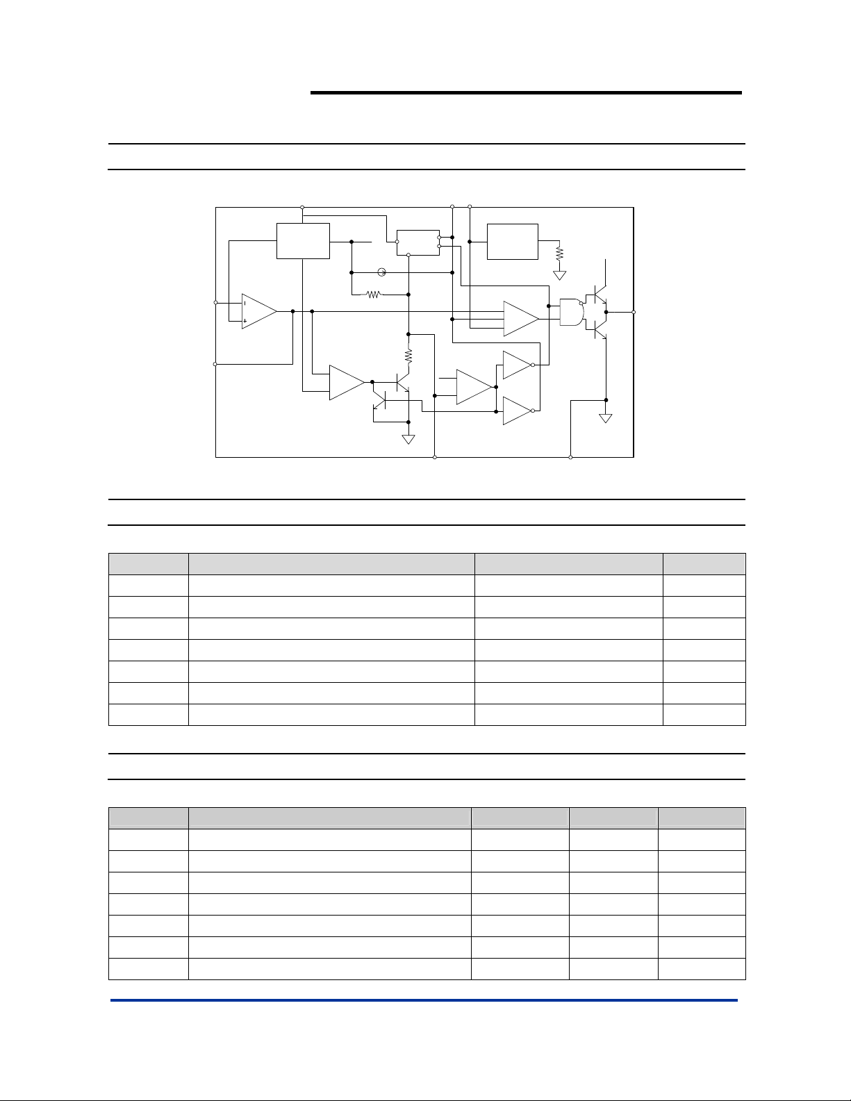
The AP2008 integrates Pulse-Width-Modulation (PWM) control
circuit into a single chip, mainly designs for power-supply
regulator. All the functions include an on-chip 0.77V reference
output, an error a mplifier, an adjustable oscillator, a soft -start,
UVLO, SCP circuitry, and a push-pull output circuit. Switching
frequency is adjustable by trimming CT. During low VCC situation,
the UVLO makes sure that the outputs are off until the internal
circuit is operational normally.
Package PackingLead Free
S : SOP-8L
L : Lead Free
G : Green
Device
AP2008SL-13 S SOP-8L 2500/Tape & Reel -13
Lead-free
Package
Code
Packaging
(Note 2)
AP2008SG-13 S SOP-8L 2500/Tape & Reel -13
Notes: 1. EU Directive 2002/95/EC (RoHS). All applicable RoHS exemptions applied. Please visit our website at
http://www.diodes.com/products/lead_free.html
2. Pad layout as shown on Diodes Inc. suggested pad layout document AP02001, which can be found on our website at
http://www.diodes.com/datasheets/ap02001.pdf
.
.
AP2008 Rev. 2 1 of 8 FEBRUARY 2009
www.diodes.com © Diodes Incorporated
13 : Tape & Reel
13” Tape and Reel
Quantity Part Number Suffix

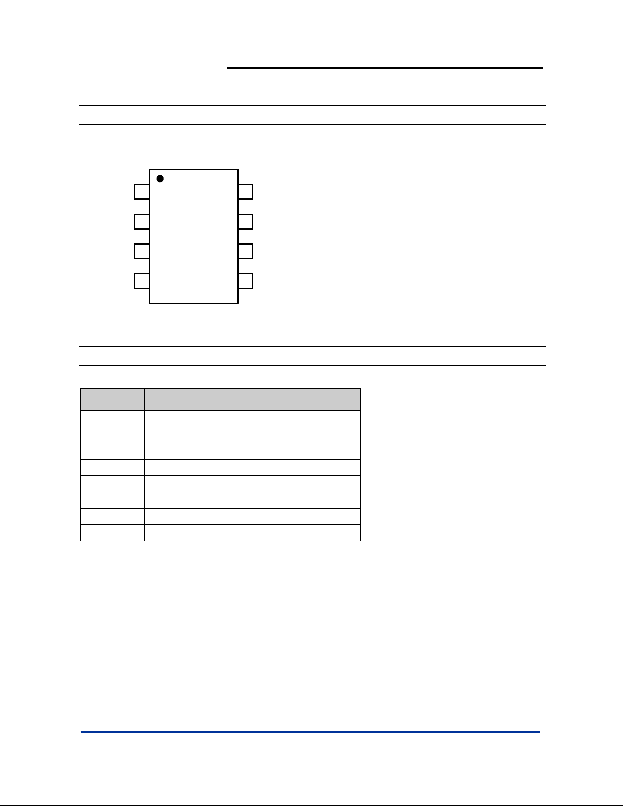
Pin Assignments
( Top View )
AP2008
PWM BUCK CONTROLLER
OUT
VCC
COMP
FB
1
2
3
4
8
7
6
5
SOP-8L
Pin Descriptions
Pin Name Description
OUT PWM Output
VCC Supply Voltage
COMP Feedback Loop Compensation
FB Voltage Feedback
SCP Short Circuit Protection
SS Soft-Start.
CT Timing Capacitor
GND Ground
GND
CT
SS
SCP
AP2008 Rev. 2 2 of 8 FEBRUARY 2009
www.diodes.com © Diodes Incorporated

Block Diagram
0.77V
VCC
Bandgap
Reference
2.5V
Internal use
UVLO
SS
CT
10K-300KHz / CT value
Oscillator
AP2008
PWM BUCK CONTROLLER
VCC
FB
COMP
Error Amplifier
1.5V
Iss
-
+
0.7V
SCP
-
+
PWM Amplifier
+
+
-
GND
OUT
Absolute Maximum Ratings
Symbol Parameter Rating Unit
VCC Supply voltage 22 V
VI Amplifier input voltage 20 V
VO Collector output voltage VCC-1.0V V
I
Source current 200 mA
SOURCE
I
Sink current 200 mA
SINK
TOP Operati n g t em p e r ature range -20 to +85
T
Storage temperature range -65 to +150
ST
Recommended Operating Conditions
Symbol Parameter Min Max Unit
VCC Supply voltage 3.6 20 V
VI Amplifier input voltage 1.05 1.45 V
VO Collector output voltage Vcc-1.5 V
IFB Current into feedback terminal 45 µA
RF Feedback resistor 100 kΩ
CT Timing capacitor 100 6800 pF
F
Oscillator frequency 10 300 KHz
OSC
o
C
o
C
AP2008 Rev. 2 3 of 8 FEBRUARY 2009
www.diodes.com © Diodes Incorporated
 Loading...