

Page 1
Off-line Primary Side Regulation Controller for Dimmable LED Driver AP1681
Preliminary Datasheet
General Description
The AP1681 is a powerful high performance AC/DC
power supply controller for dimmable LED lighting
applications. The device uses Pulse Frequency
Modulation (PFM) technology to regulate output
current according to the wall dimmer conduct angle.
The AP1681 achieves wide dimming range without
visible flicker and is compatible with diverse
dimmers.
The AP1681 features low start-up current, low
operation current and high efficiency. It also has rich
protection functions including over voltage, short
circuit, over current and over temperature protections.
The AP1681 is available in SOIC-8 package.
Features
• Primary Side Control for Output Current
Regulation Without Opto-coupler and Secondary
CV/CC Control Circuitry
• Adjustable Full Brightness and Full Dimming
Setting
• Wide Dimming Range From 100% to 1%, Down
to Full Darkness
• Adjustable Dimming Curve for Human Eye
Sensitivity
• No Visible Flicker
• Connectivity with Analog / Digital / Hybrid
Dimming Mode
• Built-in Acceleration Start
• Adjustable Soft-start Timing
• CV Open-load Regulation and Reload Detection
• Over Voltage an d Short Circuit Protection
• Over Temperature Protection
• Over Current Protection
• Maximum Switch On-time Protection
Applications
• Dimmable LED Driver Suit for Leading-edge
Dimmer, Trailing-edge Dimmer, R Type, R-C
Type or R-L Type Dimmer
SOIC-8
Figure 1. Package Type of AP1681
Jul. 2011 Rev. 1. 2 BCD Semiconductor Manufacturing Limited
1
Page 2
Preliminary Datasheet
Off-line Primary Side Regulation Controller for Dimmable LED Driver AP1681
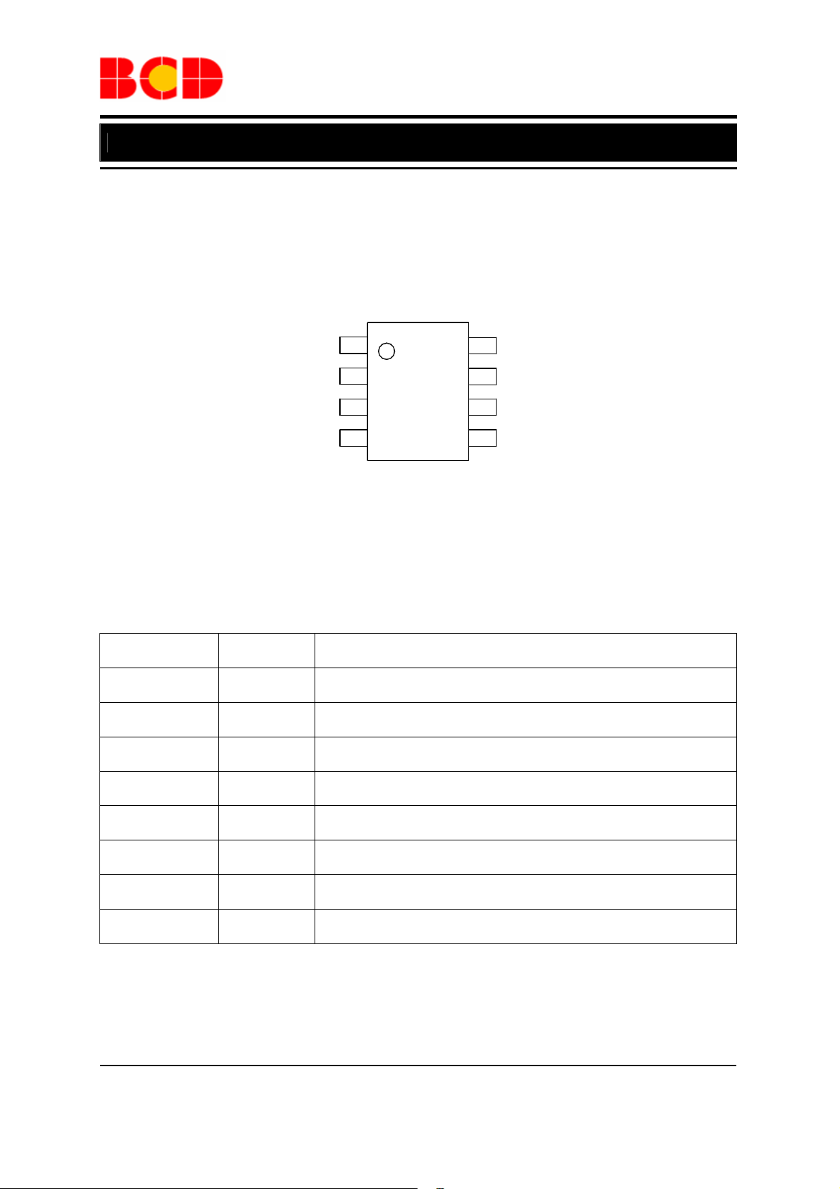
Pin Configuration
M Package
(SOIC-8)
DIM
RD
8
1
2
VCC
7
OUT
RI
FB
3
4
GND
6
5
CS
Figure 2. Pin Configuration of AP1681 (Top View)
Pin Description
Pin Number Pin Name Function
1
2
3
4
DIM Dimming control signal input
RD Full brightness level setting
RI Full dimming level setting
FB The feedback voltage sensing from the auxiliary winding
5
6
7
8
CS Primary current sensing
GND Ground. Current return for gate driver and control circuits of the IC
OUT Gate driver output
VCC Supply voltage of gate driver and control circuits of the IC
Jul. 2011 Rev. 1. 2 BCD Semiconductor Manufacturing Limited
2
Page 3
Preliminary Datasheet
Off-line Primary Side Regulation Controller for Dimmable LED Driver AP1681
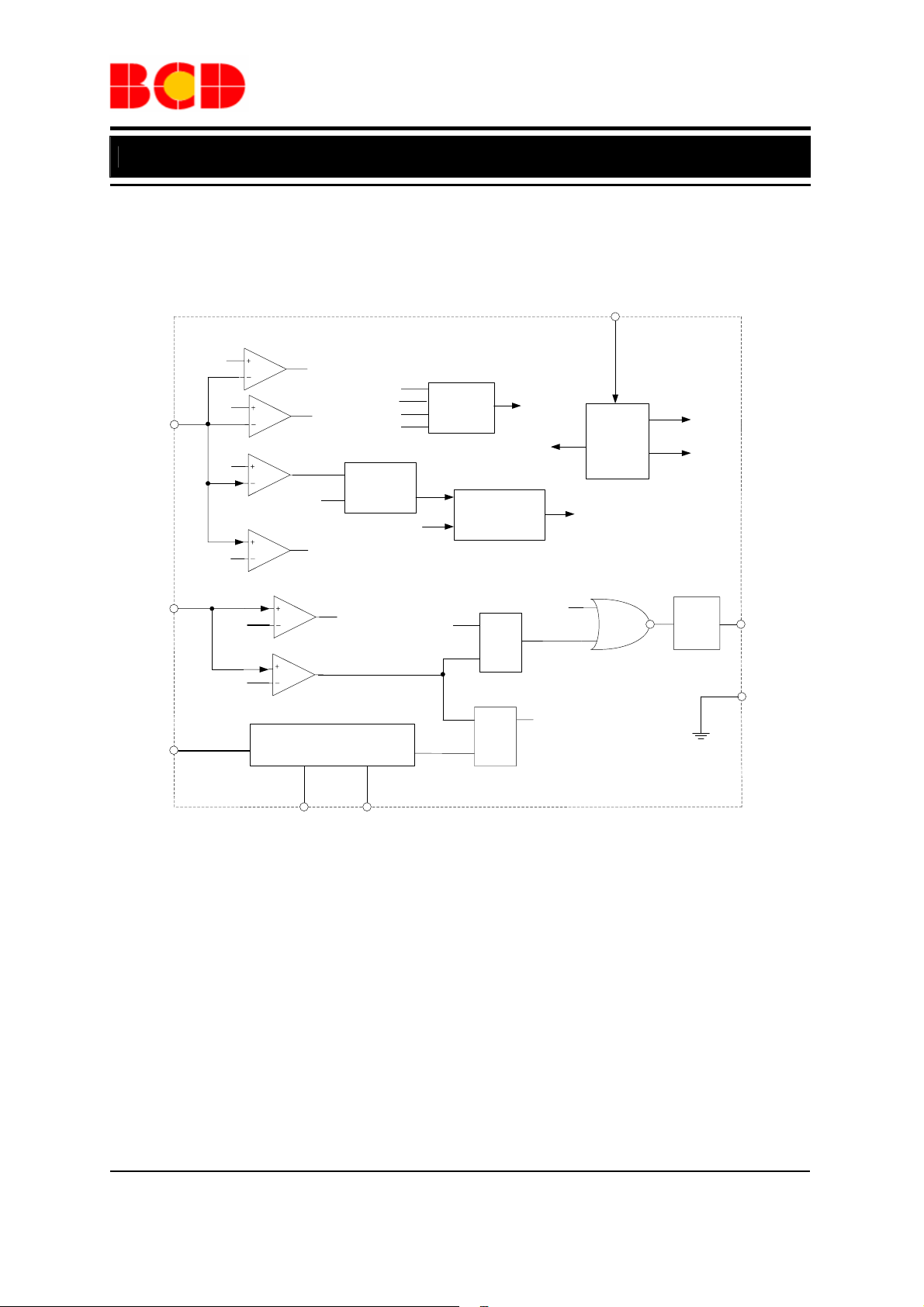
Functional Block Diagram
VCC
8
FB_OVP8V
COMP
FB
SHORT_OCP
1.75V
4
0.1V
4V
COMP
COMP
COMP
FB_ACC
Demag
CC_CTRL
CV_CTRL
VCC_OVP
FB_OVP
OTP
Tonsec
Detector
Protection
& Latch
Tons
CC_CTRL
pro
Constant
Current
Control
VCC_OVP
CC_ON
Regulator
&
Bias
Reference
UVLO
CS
DIM
5
COMP
4V
0.5V
1
COMP
SHORT_OCP
PEAK_CTRL
Dimming Control
23
RD
RI
CC_ON
R
Q
S
Q
S
R
Figure 3. Functional Block Diagram of AP1681
pro
CC_CTRL
pfm
Driver
6
7
OUT
GND
Jul. 2011 Rev. 1. 2 BCD Semiconductor Manufacturing Limited
3
Page 4
Preliminary Datasheet
Off-line Primary Side Regulation Controller for Dimmable LED Driver AP1681
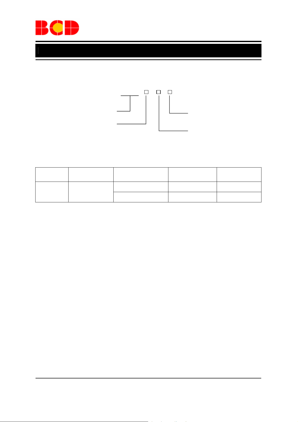
Ordering Information
AP1681 -
Package
Circuit Type
Package
M: SOIC-8
Temperature
Range
Part Number Marking ID Packing Type
G1: Green
TR: Tape & Reel
Blank: Tube
SOIC-8
-40 to 105°C
AP1681M-G1 1681M-G1 Tube
AP1681MTR-G1 1681M-G1 Tape & Reel
BCD Semiconductor's Pb-free products, as designated with "G1" suffix in the part number, are RoHS compliant
and green.
Jul. 2011 Rev. 1. 2 BCD Semiconductor Manufacturing Limited
4
Page 5

Preliminary Datasheet
Off-line Primary Side Regulation Controller for Dimmable LED Driver AP1681
Absolute Maximum Ratings (Note 1)
Parameter Symbol Value Unit
Power Supply Voltage
Driver Output Current I
Voltage at RD, RI, DIM, CS
FB Input Voltage
Operating Junction Temperature TJ 150 ºC
Storage Temperature T
Lead Temperature (Soldering, 10 sec) T
Power Dissipation at TA=50°C
Thermal Resistance
(Junction-to-Ambient)
ESD (Machine Model) 200 V
ESD (Human Body Model) 4000 V
V
CC
±300 mA
OUT
V
, VRI,
RD
V
, VCS
DIM
V
FB
-65 to 150 ºC
STG
300 ºC
LEAD
0.65 W
P
D
θ
JA
-0.3 to 30 V
-0.3 to 7 V
-40 to 10 V
150
°C/W
Note 1: Stresses greater than those listed under “Absolute Maximum Ratings” may cause permanent damage to
the device. These are stress ratings only, and functional operation of the device at these or any other conditions
beyond those indicated under “Recommended Operating Conditions” is not implied. Exposure to “Absolute
Maximum Ratings” for extended periods may affect device reliability.
Recommended Operating Conditions
Parameter Symbol Min Max Unit
Power Supply Voltage
Ambient Temperature TA -40 105 ºC
10.8 21.5 V
V
CC
Jul. 2011 Rev. 1. 2 BCD Semiconductor Manufacturing Limited
5
Page 6

Preliminary Datasheet
Off-line Primary Side Regulation Controller for Dimmable LED Driver AP1681
Electrical Characteristics
V
=15V, TA=25°C, unless otherwise specified.
CC
Parameter Symbol Conditions Min Typ Max Unit
UVLO Section
Start-up Threshold VTH (ST) 16.5 19 21.5
Minimal Operating Voltage V
(Min) After turn on 7.2 9 10.8
OPR
Standby Curr ent Section
Start-up Current IST
V
Before start up
CC=VTH
(ST)-0.5V,
1.7 10
Operating Current ICC Static 700 900 1100
V
µA
Drive Output Section
=12V
=20mA
=12V
=20V
=0 to V
=10mA
=20mA
=5mA
CC–ON
8 V
1 V
11 13 15 V
1 V
µs
I
Output High Level Voltage VOH
Output Low Level Voltage VOL
Output Voltage Rise Time tR C
Output Voltage Fall Time tF C
Output Clamp Vo ltage V
UVLO Saturation Voltage V
Maximum Switch On-time t
O-CLAMP
UVLO
ONP_MAX
GD-SOURCE
V
CC
I
GD-SINK
V
CC
=1nF 120 220 320 ns
L
=1nF 30 50 90 ns
L
I
GD-SOURCE
V
CC
V
I
SINK
CC
16.5
DIM Input Section
Voltage Gain to RI
∆V
RI
/∆V
DIM
Internal Source Current 11 20 35
-1.2 -1.1 -1.0
µA
Reload Threshold 0.8 1 1.25 V
RD and RI Section
RD Pin Voltage VRD 1.3 1.5 1.75 V
Maximum RD Current
150
µA
Maximum RI Current
250
µA
Current Sense Section
Current Sense Voltage VCS 450 500 560 mV
Maximum CS Current V
=0 120
DIM
µA
Leading Edge Blanking 600 ns
Jul. 2011 Rev. 1. 2 BCD Semiconductor Manufacturing Limited
6
Page 7

Preliminary Datasheet
Off-line Primary Side Regulation Controller for Dimmable LED Driver AP1681
Electrical Characteristics (Continued)
V
=15V, TA=25°C, unless otherwise specified.
CC
Parameter Symbol Conditions Min Typ Max Unit
Feedback Input Section
CV Feedback Threshold V
FB Pin Input Leakage
Current
Acceleration Start
Threshold
Over Voltage Protection V
3.0 4.0 5.0 V
FB-CV
V
I
FB
=4V 1.0 2 3.0
FB
µA
1.35 1.75 2.15 V
6.5 8 9.5 V
FB-OVP
Over Temperatur e Protection Section
Shutdown Temperature 140
Temperature Hysteresis 20
o
C
o
C
Typical Performance Characteristics
19.0
18.8
18.6
18.4
Start-up Voltage (V)
18.2
18.0
-40 -20 0 20 40 60 80 100 120
Ambient Temperature (oC)
Figure 4. Start-up Voltage vs. Ambient Temperature Figure 5. Minimal Operating Voltage vs.
10.0
9.5
9.0
Minimal Operating Voltage (V)
8.5
-40 -20 0 20 40 60 80 100 120
Ambient Temperature (oC)
Ambient Temperature
Jul. 2011 Rev. 1. 2 BCD Semiconductor Manufacturing Limited
7
Page 8

Preliminary Datasheet
Off-line Primary Side Regulation Controller for Dimmable LED Driver AP1681
Typical Performance Characteristics (Continued)
2.2
2.0
1.8
Start-up Current (µA)
1.6
940
920
900
880
860
840
Operating Current (µA)
820
1.4
-40 -20 0 20 40 60 80 100 120
Ambient Temperature (oC)
800
-40 -20 0 20 40 60 80 100 120
Ambient Temperature (oC)
Figure 6. Start-up Current vs. Ambient Temperature
Figure 7. Operating Current vs. Ambient Temperature
1000
900
800
700
600
500
400
300
Operating Current (µA)
200
100
0
0 5 10 15 20 25 30
Supply Voltage (V)
Figure 8. Operating Current vs. Supply Voltage Figure 9. Current Sense Voltage vs. Supply Voltage
540
520
500
480
Current Sense Voltage (mV)
460
20 22 24 26 28 30
Supply Voltage (V)
Jul. 2011 Rev. 1. 2 BCD Semiconductor Manufacturing Limited
8
Page 9

Preliminary Datasheet
Off-line Primary Side Regulation Controller for Dimmable LED Driver AP1681
Typical Performance Characteristics (Continued)
530
520
510
500
490
Current Sense Voltage (mV)
480
470
-40 -20 0 20 40 60 80 100 120
Ambient Temperature (oC)
Figure 10. Current Sense Voltage vs.
Ambient Temperature Ambient Temperature
4.3
4.2
4.1
4.0
3.9
3.8
CV Feedback Threshold (V)
3.7
3.6
20 22 24 26 28 30
Figure 12. CV Feedback Threshold vs. Figure 13. Over Voltage Protection vs.
Supply Voltage
Supply Voltage (V)
4.4
4.3
4.2
4.1
4.0
CV Feedback Threshold (V)
3.9
3.8
-40-200 20406080100120
Ambient Temperature (oC)
Figure 11. CV Feedback Threshold vs.
9.0
8.9
8.8
8.7
8.6
8.5
8.4
8.3
Over Voltage Protection (V)
8.2
8.1
8.0
-40 -20 0 20 40 60 80 100 120
Ambient Temperature (oC)
Ambient Temperature
Jul. 2011 Rev. 1. 2 BCD Semiconductor Manufacturing Limited
9
Page 10

Preliminary Datasheet
Off-line Primary Side Regulation Controller for Dimmable LED Driver AP1681
Typical Performance Characteristics (Continued)
3.0
15
2.5
2.0
1.5
FB Input Leakage Current (µA)
1.0
-40 -20 0 20 40 60 80 100 120
Ambient Temperature (oC)
Figure 14. FB Input Leakage Current vs. Figure 15. Output Clamp Voltage vs.
Ambient Temperature Supply Voltage
14
13
12
Output Clamp Voltage (V)
11
10
20 22 24 26 28 30
Supply Voltage (V)
1.70
1.65
1.60
1.55
RD Pin Voltage (V)
1.50
1.45
-40-200 20406080100120
Ambient Temperature (oC)
Figure 16. RD Pin Voltage vs. Ambient Temperature
Jul. 2011 Rev. 1. 2 BCD Semiconductor Manufacturing Limited
10
Page 11

Preliminary Datasheet
Off-line Primary Side Regulation Controller for Dimmable LED Driver AP1681
Typical Application
COMP
EE16
L=1.43mH
47k
ZCD
GD
CS
INV
AP1661
115T
11T
47
3N60
V
BUS
+
100pF
2R
630V
6.8 F
350V
120Vac
60Hz
Dimmer
EE16
L=4.5mH
47nF
~
~
1A/600V
V
REC
+
22nF
470k
560k
3.3k
1nF
GND
MULT
VCC
560k
AP1681 LED Application:
Dimmable LED Driver
Input: 120Vac/60Hz
18W Power
Output: 8 LEDs, 26V
5.0mA to 550mA
32 V
OPEN
LOAD
680k
220k
270k
1
F
330k 330k
100k
16k
0.47
0.47
F
0.47
F
VCC
DIM
F
RD
51k 100k
BAV20
BAV20
RI
47k
FB
OUT
CS
GND
330nF
14T
=0.3
φ
10k
AP1681
16k
2.2nF
630V
Figure 17. Typical Application of AP1681
100
3.0k
680k
68k
680k
0.16
FR105
95T
×3
SR
3A/150V
19T
=0.4
φ
TIW
EF20
L=2.54mH
4N60
1.3R
220
F
35V
+
Y2
1.5nF 3kV
27k
V
OUT
Jul. 2011 Rev. 1. 2 BCD Semiconductor Manufacturing Limited
11
Page 12

Preliminary Datasheet
Off-line Primary Side Regulation Controller for Dimmable LED Driver AP1681
Mechanical Dimensions
SOIC-8 Unit: mm(inch)
R0.150(0.006)
Jul. 2011 Rev. 1. 2 BCD Semiconductor Manufacturing Limited
12
Page 13

BCD Semiconductor Manufacturing Limited
IMPORTANT NOTICE
IMPORTANT NOTICE
BCD Semiconductor Manufacturing Limited reserves the right to make changes without further notice to any products or specifi-
BCD Semiconductor Manufacturing Limited reserves the right to make changes without further notice to any products or specifi-
cations herein. BCD Semiconductor Manufacturing Limited does not assume any responsibility for use of any its products for any
cations herein. BCD Semiconductor Manufacturing Limited does not assume any responsibility for use of any its products for any
particular purpose, nor does BCD Semiconductor Manufacturing Limited assume any liability arising out of the application or use
particular purpose, nor does BCD Semiconductor Manufacturing Limited assume any liability arising out of the application or use
of any its products or circuits. BCD Semiconductor Manufacturing Limited does not convey any license under its patent rights or
of any its products or circuits. BCD Semiconductor Manufacturing Limited does not convey any license under its patent rights or
other rights nor the rights of others.
other rights nor the rights of others.
http://www.bcdsemi.com
MAIN SITE
MAIN SITE
- Headquarters
BCD Semiconductor Manufacturing Limited
BCD Semiconductor Manufactur ing Limited
- Wafer Fab
No. 1600, Zi Xing Road, Shanghai ZiZhu Science-based Industrial Park, 200241, China
Shanghai SIM-BCD Semiconductor Manufacturing Limited
Tel: +86-21-24162266, Fax: +86-21-24162277
800, Yi Shan Road, Shanghai 200233, China
Tel: +86-21-6485 1491, Fax: +86-21-5450 0008
REGIONAL SALES OFFICE
Shenzhen Office
REGIONAL SALES OFFICE
Shanghai SIM-BCD Semiconductor Manufacturing Co., Ltd., Shenzhen Office
Shenzhen Office
Unit A Room 1203, Skyworth Bldg., Gaoxin Ave.1.S., Nanshan District, Shenzhen,
Shanghai SIM-BCD Semiconductor Manufacturing Co., Ltd. Shenzhen Office
China
Advanced Analog Circuits (Shanghai) Corporation Shenzhen Office
Tel: +86-755-8826 7951
Room E, 5F, Noble Center, No.1006, 3rd Fuzhong Road, Futian District, Shenzhen 518026, China
Fax: +86-755-8826 7865
Tel: +86-755-8826 7951
Fax: +86-755-8826 7865
- Wafer Fab
BCD Semiconductor Manufacturing Limited
Shanghai SIM-BCD Semiconductor Manufacturing Co., Ltd.
- IC Design Group
800 Yi Shan Road, Shanghai 200233, China
Advanced Analog Circuits (Shanghai) Corporation
Tel: +86-21-6485 1491, Fax: +86-21-5450 0008
8F, Zone B, 900, Yi Shan Road, Shanghai 200233, China
Tel: +86-21-6495 9539, Fax: +86-21-6485 9673
Taiwan Office
BCD Semiconductor (Taiwan) Company Limited
Taiwan Office
4F, 298-1, Rui Guang Road, Nei-Hu District, Taipei,
BCD Semiconductor (Taiwan) Company Limited
Tai wan
4F, 298-1, Rui Guang Road, Nei-Hu District, Taipei,
Tel: +886-2-2656 2808
Taiwan
Fax: +886-2-2656 2806
Tel: +886-2-2656 2808
Fax: +886-2-2656 2806
USA Office
BCD Semiconductor Corp.
USA Office
30920 Huntwood Ave. Hayward,
BCD Semiconductor Corporation
CA 94544, USA
30920 Huntwood Ave. Hayward,
Tel : +1-510-324-2988
CA 94544, U.S.A
Fax: +1-510-324-2788
Tel : +1-510-324-2988
Fax: +1-510-324-2788
 Loading...