

Page 1
Data Sheet
HIGH PERFORMANCE POWER FACTOR CORRECTOR AP1662
General Description
The AP1662 is an active power factor control IC
which is designed mainly for use as a pre-converter
in electronic ballast, AC-DC adapter and off-line
SMPS applications.
.
The IC includes an internal start-up timer for
stand-alone applications, a one-quadrant multiplier to
realize near unity power factor and a zero current
detector to ensure DCM boundary conduction
operation.
The totem pole output stage is capable of driving
power MOSFET with 600mA source current and
800mA sink current.
Designed with advanced BiCMOS process, the
AP1662 features low start-up current, low operation
current and low power dissipation. The AP1662 also
has rich protection features including over-voltage
protection, input under-voltage lockout with
hysteresis and multiplier output clamp to limit
maximum peak current.
The AP1662 meets IEC61000-3-2 standard even at
one-quadrant load and THD lower than 10% at
high-end line voltage and full load.
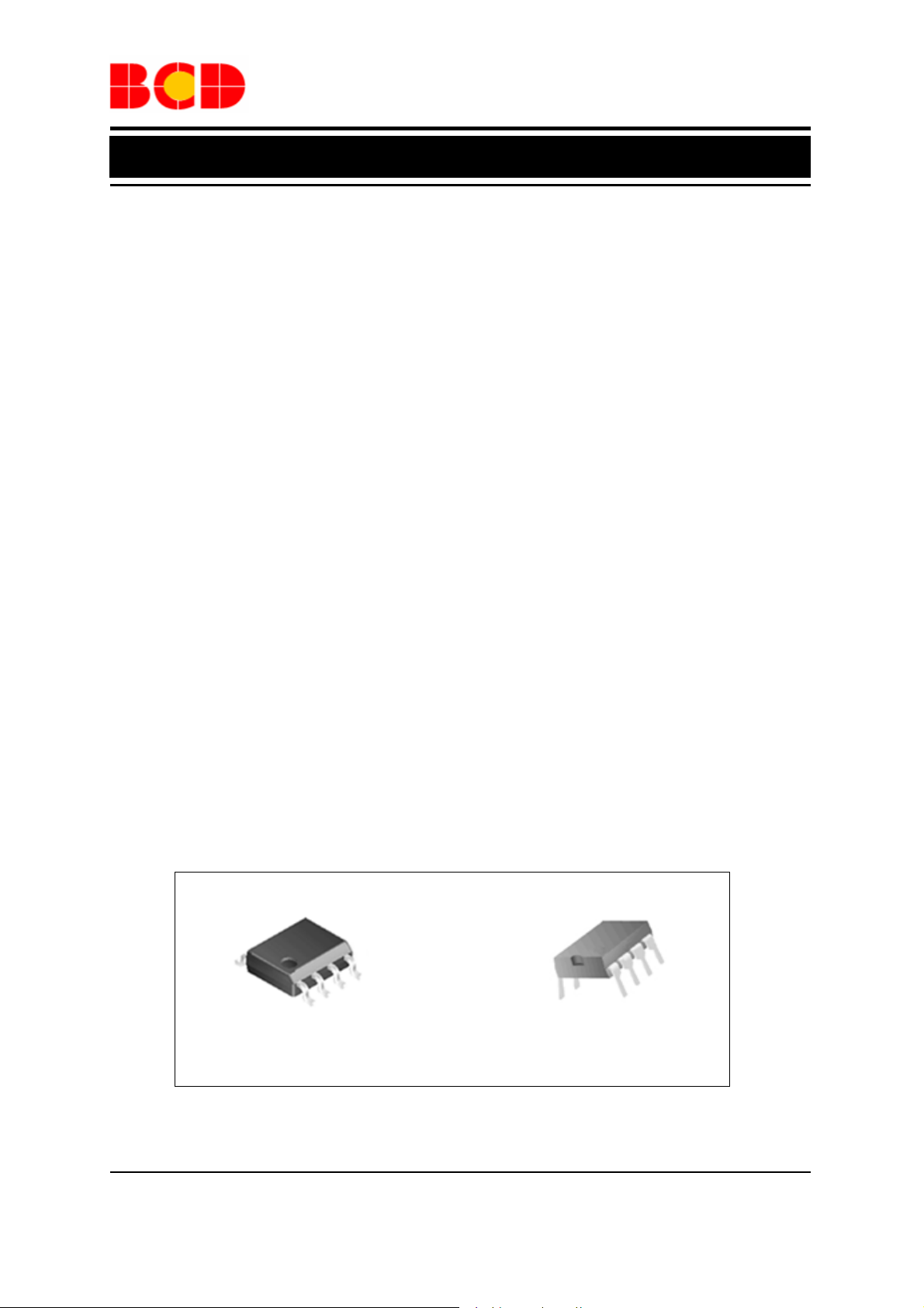
The IC is available in SOIC-8 and DIP-8 packages.
Features
Comply with IEC61000-3-2 Standard
•
• Proprietary Design for Minimum THD
• Zero Current Detection Control for DCM
Boundary Conduction Mode
• Adjustable Output Voltage with Precise
Over-voltage Protection
• Low Start-up Current with 40µA Typical Value
• Low Quiescent Current with 2.5mA Typical
Va lu e
• 1% Precision Internal Reference Voltage @
T
=25°C
J
• Internal Start-up Timer
• Disable Function for Reduced Current
Consumption
• Totem Pole Output with 600mA Source and
800mA Sink Current Capability
• Under-voltage Lockout with 2.5V Hysteresis
Applications
• Electronic Ballast
• AC-DC Adapter
• Off-line SMPS
• Single Stage PFC LED Driver
SOIC-8 DIP-8
Figure 1. Package Types of AP1662
Jul. 2012 Rev. 1. 3 BCD Semiconductor Manufacturing Limited
1
Page 2

Data Sheet
HIGH PERFORMANCE POWER FACTOR CORRECTOR AP1662
Pin Configuration
M Package
(SOIC-8)
INV VCC
1
8
COMP GD
2
7
MULT GND
3
6
CS ZCD
4
5
P Package
(DIP-8)
INV VCC
1
8
COMP GD
2
7
MULT GND
3
6
CS ZCD
4
5
Figure 2. Pin Configuration of AP1662 (Top View)
Jul. 2012 Rev. 1. 3 BCD Semiconductor Manufacturing Limited
2
Page 3
Data Sheet
HIGH PERFORMANCE POWER FACTOR CORRECTOR AP1662
Pin Description
Pin Number Pin Name Function
1 INV Inverting input of the error amplifier
2 COMP Output of the error amplifier
3 MULT Input of the multiplier
4 CS Input of the current control loop comparator
5 ZCD
6 GND
7 GD Gate driver output
Zero current detection input. If it is connected to GND, the
device is disabled
Ground. Current return for gate driver and control circuits of
the IC
8 VCC Supply voltage of gate driver and control circuits of the IC
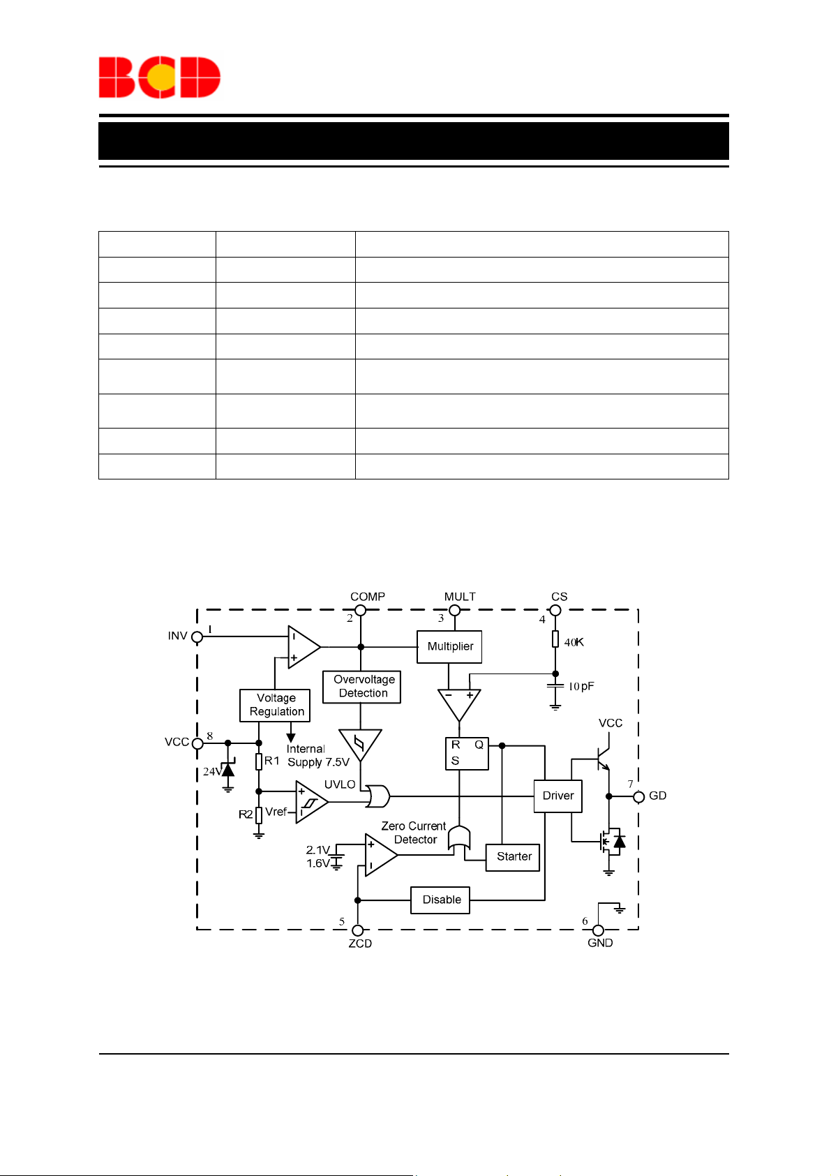
Functional Block Diagram
Figure 3. Functional Block Diagram of AP1662
Jul. 2012 Rev. 1. 3 BCD Semiconductor Manufacturing Limited
3
Page 4
Data Sheet
HIGH PERFORMANCE POWER FACTOR CORRECTOR AP1662
Ordering Information
AP1662 -
Circuit Type E1: Lead Free
Package
SOIC-8
G1: Green
Package Blank: Tube
M: SOIC-8
P: DIP-8
Temperature
Range
-40 to 105°C
TR: Tape & Reel
Part Number Marking ID
Lead Free Green Lead Free Green
AP1662M-E1 AP1662M-G1 1662M-E1 1662M-G1 Tube
AP1662MTR-E1 AP1662MTR-G1 1662M-E1 1662M-G1 Tape & Reel
Packing
Type
DIP-8
-40 to 105°C
AP1662P-E1 AP1662P-G1 AP1662P-E1 AP1662P-G1 Tube
BCD Semiconductor's Pb-free products, as designated with "E1" suffix in the part number, are RoHS compliant.
Products with “G1” suffix are available in green packages.
Jul. 2012 Rev. 1. 3 BCD Semiconductor Manufacturing Limited
4
Page 5
Data Sheet
HIGH PERFORMANCE POWER FACTOR CORRECTOR AP1662
Absolute Maximum Ratings (Note 1)
Parameter Symbol Value Unit
Power Supply Voltage VCC Self-limited V
Operating Supply Current ICC 30 mA
Input/Output of Error Amplifier,
Input of Multiplier
Current Sense Input VCS -0.3 to 7 V
V
INV
V
, V
MULT
COMP
,
-0.3 to 7 V
Zero Current Detector Input I
Power Dissipation and Thermal
characteristics @ T
=50°C
A
Thermal Resistance
(Junction to Ambient)
P
R
ZCD
TOT
θJA
mA
Sink 10
DIP-8 1
W
SOIC-8 0.65
DIP-8 100
ºC/W
SOIC-8 150
Operating Junction Temperature TJ -40 to 150 ºC
Source -50
Storage Temperature Range T
Lead Temperature (Soldering, 10
Seconds)
ESD (Human Body Model) V
ESD (Machine Model) V
-65 to 150 ºC
STG
260 ºC
T
LEAD
ESD(HBM)
ESD(MM)
3000 V
200 V
Note 1: Stresses greater than those listed under “Absolute Maximum Ratings” may cause permanent damage to
the device. These are stress ratings only, and functional operation of the device at these or any other conditions
beyond those indicated under “Recommended Operating Conditions” is not implied. Exposure to “Absolute
Maximum Ratings” for extended periods may affect device reliability.
Jul. 2012 Rev. 1. 3 BCD Semiconductor Manufacturing Limited
5
Page 6
Data Sheet
HIGH PERFORMANCE POWER FACTOR CORRECTOR AP1662
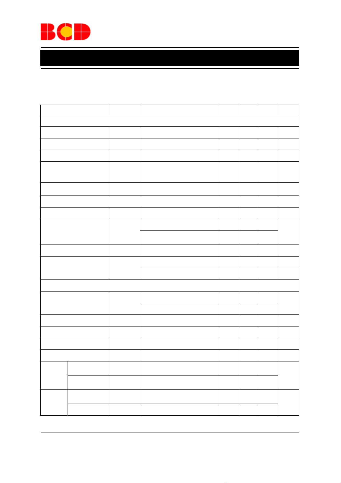
Electrical Characteristics
V
=12V, TJ =-25°C to 125°C, CO=1nF, unless otherwise specified.
CC
Parameter Symbol Test Conditions Min Typ Max Unit
Under Voltage Lockout Section
Turn-on Threshold V
Turn-off Threshold V
Hysteresis V
VCC Rising 11 12 13 V
CC-ON
VCC Falling 8.7 9.5 10.3 V
CC-OFF
2.2 2.5 2.8 V
CC-HYS
VCC Operating Range VCC After turn-on 10.3 22 V
Zener Voltage V
ICC=20mA 22 24 V
Z
Total Supply Current Section
Start-up Current I
START-UP
Operating Supply Current ICC
Quiescent Current IQ After turn on 2.5 3.75 mA
Quiescent Current IQ
VCC=11V before turn-on 40 70
Frequency=70kHz 3.5 5
In OVP condition
=2.7V
V
INV
≤150mV, VCC>V
V
ZCD
V
≤150mV, VCC<V
ZCD
CC-OFF
CC-OFF
1.4 2.2
2.2 mA
20 50 90
µA
mA
µA
Error Amplifier Section
=25ºC 2.465 2.5 2.535
T
Voltage Feedback Input
Threshold
V
INV
J
10.3V<VCC<20V 2.44 2.56
V
Line Regulation VCC=10.3V to 20V 2 5 mV
Input Bias Current I
V
INV
=0 to 3V -0.1 -1
INV
µA
Voltage Gain GV Open Loop 60 80 dB
Gain Bandwidth GB 1 MHz
Output
Voltage
Output
Current
Upper Clamp
Voltage
Lower Clamp
Voltage
Source
Current
Sink Current I
V
V
I
COMP-H
COMP-L
COMP-H
COMP-L
I
SOURCE
I
SINK
V
COMP
V
COMP
=0.5mA 5.15 5.55 5.85
V
=0.5mA 2.1 2.25 2.4
=4V, V
=2.4V -2 -4 -8
INV
mA
=4V, V
=2.6V 2.5 4.5
INV
Jul. 2012 Rev. 1. 3 BCD Semiconductor Manufacturing Limited
6
Page 7

Data Sheet
HIGH PERFORMANCE POWER FACTOR CORRECTOR AP1662
Electrical Characteristics (Continued)
V
=12V, TJ =-25°C to 125°C, CO=1nF, unless otherwise specified.
CC
Parameter Symbol Test Conditions Min Typ Max Unit
Multiplier Section
Linear Input Voltage
Range
Output Maximum
Slope
△V
0 to 3
V
MULT
△ VCS/
MULT
Gain k V
Current Sense Section
V
: 0 to 0.5V,
MULT
=Upper Clamp Voltage
V
COMP
=1V, V
MULT
COMP
1.65 1.9
=4V 0.6 0.75 0.9 1/V
0 to
3.5
V
Input Bias Current ICS VCS=0V -1
V
Current Sense Offset
Voltage
Current Sense
Reference Clamp
V
V
Delay to Output t
CS-OFFSET
CS-CLAMP
d(H-L
) 200 350
=0V 30
MULT
V
=2.5V 5
MULT
= Upper Clamp
V
COMP
Voltage, V
MULT
= 2.5V
1.6 1.7 1.8
µA
mV
V
ns
Zero Current Detection Section
Arming Voltage
(positive-going edge)
Triggering Voltage
(negative-going edge)
Upper Clamp Voltage V
Lower Clamp Voltage
Source Current
Capability
Sink Current
Capability
Sink Bias Current I
(Note 2) 2.1
V
ZCDA
(Note 2) 1.6
V
ZCDT
=20µA 4.5 5.1 5.9
I
ZCD
ZCD-H
V
ZCD-L
I
ZCD-SR
I
ZCD-SN
ZCD-B
I
=3mA 4.7 5.2 6.1
ZCD
I
= -3mA 0.3 0.65 1
ZCD
-2.5 -10
3
1V ≤ V
≤ 4.5 V 2
ZCD
V
V
V
V
mA
mA
µA
Disable Threshold V
Disable Hysteresis V
Restart Current After
Disable
ZCD-DIS
ZCD-HYS
I
ZCD-RES
150 200 250
100
V
ZCD<VDIS
, VCC>V
-80 -120
CC-OFF
mV
mV
µA
Note 2: Limits over the full temperature are guaranteed by design, but not tested in production.
Jul. 2012 Rev. 1. 3 BCD Semiconductor Manufacturing Limited
7
Page 8

K
Data Sheet
HIGH PERFORMANCE POWER FACTOR CORRECTOR AP1662
Electrical Characteristics (Continued)
V
=12V, TJ =-25°C to 125°C, CO=1nF, unless otherwise specified.
CC
Parameter Symbol Test Conditions Min Typ Max Unit
Drive Output Section
I
GD-SOURCE
V
Dropout Voltage
Output Voltage Rise
Time
Output Voltage Fall Time tF 30 70
Output Clamp Voltage V
UVLO Saturation VOS
OH
VOL I
t
R
O-CLAMP
I
GD-SOURCE
GD-SINK
40 80
I
GD-SOURCE
V
CC
V
CC
I
SIN
=200mA 2.5 3
=20mA 2 2.8
=200mA 0.9 1.9
=20V
=0 to V
=10mA
=5mA
CC-ON
,
9 11 13
1.1
Output Over Voltage Section
OVP Triggering Current I
Static OVP Threshold V
OVP
OVP_TH
35 40 45 µA
2.1 2.25 2.4
Starter
Start Timer Period t
START
75 130 300
V
ns
ns
V
V
V
µs
Jul. 2012 Rev. 1. 3 BCD Semiconductor Manufacturing Limited
8
Page 9

Data Sheet
HIGH PERFORMANCE POWER FACTOR CORRECTOR AP1662
Typical Performance Characteristics
3.0
2.5
2.0
1.5
1.0
Supply Current (mA)
0.5
0.0
0 5 10 15 20 25
Supply Voltage (V)
CO=1nF
f=70kHz
=25oC
T
J
12.5
12.0
11.5
11.0
10.5
Voltage (V)
10.0
9.5
9.0
-50 0 50 100 150
V
CC-OFF
Junction Temperature (oC)
V
CC-ON
Figure 4. Supply Current vs. Supply Voltage Figure 5. Start-up & UVLO vs. T
8
4
2
1
(mA)
CC
I
0.0625
0.03125
VCC=12V
0.5
C
=1nF
O
0.25
f=70kHz
0.125
-50 0 50 100 150
Junction Temperature (
Quiescent
Disabled or during OVP
Before start-up
o
C)
28
27
26
(V)
25
CC-CLAMP
V
24
23
22
-50 0 50 100 150
Junction Temperature (oC)
Figure 6. ICC Consumption vs. TJ Figure 7. VCC Zener Voltage vs. TJ
J
Jul. 2012 Rev. 1. 3 BCD Semiconductor Manufacturing Limited
9
Page 10

Data Sheet
HIGH PERFORMANCE POWER FACTOR CORRECTOR AP1662
Typical Performance Characteristics (Continued)
2.60
2.55
2.50
(V)
REF
V
2.45
2.40
-50 0 50 100 150
Junction Temperature (
Figure 8. Feedback Reference Voltage vs. TJ Figure 9. OVP Current vs. T
500
400
300
(ns)
200
d(H-L)
t
100
0
-50 0 50 100 150
Junction Temperature (
Figure 10. Delay-to-Output vs. TJ Figure 11. E/A Output Clamp Levels vs. TJ
VCC=12V
O
C)
VCC=12V
o
C)
43.0
42.5
42.0
41.5
41.0
(µA)
OVP
I
40.5
40.0
39.5
39.0
-50 0 50 100 150
Junction Temperature (
6.0
5.5
5.0
4.5
(V)
4.0
COMP
V
3.5
3.0
2.5
2.0
-50 0 50 100 150
Upper Clamp
Lower Clamp
Junction Temperature (oC)
VCC=12V
o
C)
J
VCC=12V
Jul. 2012 Rev. 1. 3 BCD Semiconductor Manufacturing Limited
10
Page 11

Data Sheet
HIGH PERFORMANCE POWER FACTOR CORRECTOR AP1662
Typical Performance Characteristics (Continued)
2.0
1.0
1.8
1.6
(V)
1.4
CS-CLAMP
V
1.2
1.0
-50 0 50 100 150
Junction Temperature (
VCC=12V
V
COMP
o
C)
=Upper Clamp
0.8
VCC=12V
V
=4V
0.6
0.4
Multiplier Gain
0.2
0.0
-50 0 50 100 150
Junction Temperature (
COMP
V
=1V
MULT
o
C)
Figure 12. V
CS-CLAMP
0
-2
-4
(mA)
ZCD
I
-6
-8
-50 0 50 100 150
Junction Temperature (
Figure 14. ZCD Source Capability vs. TJ Figure 15. ZCD Clamp Levels vs. TJ
vs. TJ Figure 13. Multiplier Gain vs. T
VCC=12V
V
ZCD
=Lower Clamp
o
C)
7
6
5
4
(V)
ZCD
3
V
2
1
0
-50 0 50 100 150
Junction Temperature (
Upper Clamp
Lower Clamp
VCC=12V
I
= + 2.5mA
ZCD
o
C)
J
Jul. 2012 Rev. 1. 3 BCD Semiconductor Manufacturing Limited
11
Page 12

Data Sheet
HIGH PERFORMANCE POWER FACTOR CORRECTOR AP1662
Typical Performance Characteristics (Continued)
200
190
180
170
160
(µS)
START
150
t
140
130
120
-50 0 50 100 150
Junction Temperature (
1.8
VCC=12V
o
C)
1.6
1.4
1.2
1.0
(V)
CS
0.8
V
0.6
0.4
0.2
0.0
0.00.51.01.52.02.53.03.54.04.5
V
=5.0
COMP
=4.5
COMP
V
V
=MAX
COMP
V
V
=4.0
COMP
V
(V)
MULT
COMP
V
V
V
V
=3.5
COMP
COMP
COMP
COMP
=3.2
=3.0
=2.8
=2.6
Figure 16. Start-up Timer vs. TJ Figure 17. Multiplier Characteristics
I
GD
(mA)
6
5
4
(V)
3
GD
V
2
1
0
0 200 400 600 800 1000
TJ=25oC
VCC=11V
SINK
Figure 18. Gate-driver Output Low Saturation Figure 19. Gate-driver Output High Saturation
VGD (V)
V
-2.0
CC
-2.5
V
CC
-3.0
V
CC
V
-3.5
CC
V
-4.0
CC
0 100 200 300 400 500 600 700
TJ=25oC
VCC=11V
SOURCE
I
(mA)
GD
Jul. 2012 Rev. 1. 3 BCD Semiconductor Manufacturing Limited
12
Page 13

Data Sheet
HIGH PERFORMANCE POWER FACTOR CORRECTOR AP1662
Typical Performance Characteristics (Continued)
15
1.1
(V)
V
1.0
0.9
0.8
GD_OFF
0.7
0.6
14
13
(V)
12
GD_CLAMP
V
11
VCC=20V
VCC=0V
10
-50 0 50 100 150
Junction Temperature (
o
C)
0.5
-50 0 50 100 150
Junction Temperature (oC)
Figure 20. Gate-driver Clamp vs. TJ Figure 21. UVLO Saturation vs. T
J
Jul. 2012 Rev. 1. 3 BCD Semiconductor Manufacturing Limited
13
Page 14

∆
×−×
=
Data Sheet
HIGH PERFORMANCE POWER FACTOR CORRECTOR AP1662
Functional Block Description
AP1662 is a high performance power factor
correction controller which operates in DCM
boundary conduction mode. The PFC converter's
switch will be turned on when the inductor current
reduces to zero and turned off when the sensed
inductor current reaches the required reference which
is decided by the output of multiplier.
Error Amplifier and Over-Voltage
Protection
The error amplifier regulates the PFC output voltage.
The internal reference on the non-inverting input of
the error amplifier is 2.5V. The error amplifier's
inverting input (INV) is connected to an external
resistor divider which senses the output voltage. The
output of error amplifier is one of the two inputs of
multiplier. A compensation loop is connected outside
between INV and the error amplifier output.
Normally, the compensation loop bandwidth is set
very low to realize high power factor for PFC
converter.
To make the over voltage protection fast, the internal
OVP function is added. If the output over voltage
happens, excess current will flow into the output pin
of the error amplifier through the feedback
compensation capacitor. (see Figure 22) The AP1662
monitors the current flowing into the error amplifier
output pin. When the detected current is higher than
40µA, the dynamic OVP is triggered. The IC will be
Figure 22. Error Amplifier and OVP Block
disabled and the drive signal is stopped. If the output
over voltage lasts so long that the output of error
amplifier goes below 2.25V, static OVP will take
place. Also the IC will be disabled until the output of
error amplifier goes back to its linear region. R1 and
R2 (see Fig. 22) will be selected as below:
1
V
R
R
O
1
−=
5.22
V
V
OVP
40
A
µ
R
1
=
Multiplier
The multiplier has two inputs. One (Pin 3) is the
divided AC sinusoidal voltage which makes the
current sense comparator threshold voltage vary from
zero to peak value. The other input is the output of
error amplifier (Pin 2). In this way, the input average
current wave will be sinusoidal as well as reflects the
load status. Accordingly a high power factor and
good THD are achieved. The multiplier transfer
character is designed to be linear over a wide
dynamic range, namely, 0V to 3V for Pin 3 and 2V to
5.8V for Pin 2. The relationship between the
multiplier output and inputs is described as below
equation:
VVkV
)5.2(
MULTCOMPCS
where VCS (Multiplier output) is the reference for the
current sense, k is the multiplier gain, V
COMP
voltage on pin 2 (error amplifier output) and V
the voltage on pin 3.
Current Sense/Current Sense
Comparator
The PFC switch's turn-on current is sensed through
an external resistor in series with the switch. When
the sensed voltage exceeds the threshold voltage (the
multiplier output), the current sense comparator will
become low and the external MOSFET will be turned
off. This insures a cycle-by-cycle current mode
control operation. The maximum current sense
reference is 1.8V. The max value usually happens at
startup process or abnormal conditions such as short
load.
is the
is
MULT
Jul. 2012 Rev. 1. 3 BCD Semiconductor Manufacturing Limited
14
Page 15

Data Sheet
HIGH PERFORMANCE POWER FACTOR CORRECTOR AP1662
Functional Block Description
(Continued)
Zero Current Detection
AP1662 is a DCM boundary conduction current
mode PFC controller. Usually, the zero current
detection (ZCD) voltage signal comes from the
auxiliary winding of the boost inductor. When the
ZCD pin voltage decreases below 1.6V, the gate
drive signal becomes high to turn on the external
MOSFET. 500mV of hysteresis is provided to avoid
false triggering. The ZCD pin can be used for
disabling the IC. Making its voltage below 0.15V or
short to the ground will disable the device thus
reduce the IC supply current consumption.
Typical Application
Figure 23. 85 to 265V Wide Range Input 90W PFC Demo Board Electrical Schematic Circuit
Jul. 2012 Rev. 1. 3 BCD Semiconductor Manufacturing Limited
15
Page 16

Data Sheet
HIGH PERFORMANCE POWER FACTOR CORRECTOR AP1662
Mechanical Dimensions
SOIC-8 Unit: mm(inch)
4.700(0.185)
5.100(0.201)
7
°
7
°
1.270(0.050)
TYP
0.100(0.004)
0.300(0.012)
1.350(0.053)
1.750(0.069)
0.675(0.027)
0.725(0.029)
D
2
D
1
:
0
0.320(0.013)
5.800(0.228)
6.200(0.244)
0.800(0.031)
°
8
°
8
0.200(0.008)
0
°
8
°
1°
5°
0.450(0.017)
0.800(0.031)
)
6
0
0
.
0
(
0
5
1
.
0
R
1.000(0.039)
0.330(0.013)
0.510(0.020)
R0.150(0.006)
3.800(0.150)
4.000(0.157)
0.190(0.007)
0.250(0.010)
0.900(0.035)
Note: Eject hole, oriented hole and mold mark is optional.
Jul. 2012 Rev. 1. 3 BCD Semiconductor Manufacturing Limited
16
Page 17

Data Sheet
HIGH PERFORMANCE POWER FACTOR CORRECTOR AP1662
Mechanical Dimensions (Continued)
DIP-8 Unit: mm(inch)
0.700(0.028)
°
6
1.524(0.060) TYP
7.620(0.300)TYP
°
6
5°
3.710(0.146)
4.310(0.170)
3.000(0.118)
3.600(0.142)
0.254(0.010)TYP
R0.750(0.030)
Φ3.000(0.118)
Depth
0.100(0.004)
0.200(0.008)
4
°
0.360(0.014)
0.560(0.022)
0.130(0.005)MIN
9.000(0.354)
9.400(0.370)
3.200(0.126)
3.600(0.142)
0.510(0.020)MIN
2.540(0.100) TYP
6.200(0.244)
6.600(0.260)
4
0.204(0.008)
0.360(0.014)
8.200(0.323)
9.400(0.370)
Note: Eject hole, oriented hole and mold mark is optional.
Jul. 2012 Rev. 1. 3 BCD Semiconductor Manufacturing Limited
17
Page 18

BCD Semiconductor Manufacturing Limited
IMPORTANT NOTICE
IMPORTANT NOTICE
BCD Semiconductor Manufacturing Limited reserves the right to make changes without further notice to any products or specifi-
BCD Semiconductor Manufacturing Limited reserves the right to make changes without further notice to any products or specifi-
cations herein. BCD Semiconductor Manufacturing Limited does not assume any responsibility for use of any its products for any
cations herein. BCD Semiconductor Manufacturing Limited does not assume any responsibility for use of any its products for any
particular purpose, nor does BCD Semiconductor Manufacturing Limited assume any liability arising out of the application or use
particular purpose, nor does BCD Semiconductor Manufacturing Limited assume any liability arising out of the application or use
of any its products or circuits. BCD Semiconductor Manufacturing Limited does not convey any license under its patent rights or
of any its products or circuits. BCD Semiconductor Manufacturing Limited does not convey any license under its patent rights or
other rights nor the rights of others.
other rights nor the rights of others.
http://www.bcdsemi.com
MAIN SITE
MAIN SITE
- Headquarters
BCD Semiconductor Manufacturing Limited
BCD Semiconductor Manufactur ing Limited
- Wafer Fab
No. 1600, Zi Xing Road, Shanghai ZiZhu Science-based Industrial Park, 200241, China
Shanghai SIM-BCD Semiconductor Manufacturing Limited
Tel: +86-21-24162266, Fax: +86-21-24162277
800, Yi Shan Road, Shanghai 200233, China
Tel: +86-21-6485 1491, Fax: +86-21-5450 0008
REGIONAL SALES OFFICE
Shenzhen Office
REGIONAL SALES OFFICE
Shanghai SIM-BCD Semiconductor Manufacturing Co., Ltd., Shenzhen Office
Shenzhen Office
Unit A Room 1203, Skyworth Bldg., Gaoxin Ave.1.S., Nanshan District, Shenzhen,
Shanghai SIM-BCD Semiconductor Manufacturing Co., Ltd. Shenzhen Office
China
Advanced Analog Circuits (Shanghai) Corporation Shenzhen Office
Tel: +86-755-8826 7951
Room E, 5F, Noble Center, No.1006, 3rd Fuzhong Road, Futian District, Shenzhen 518026, China
Fax: +86-755-8826 7865
Tel: +86-755-8826 7951
Fax: +86-755-8826 7865
- Wafer Fab
BCD Semiconductor Manufacturing Limited
Shanghai SIM-BCD Semiconductor Manufacturing Co., Ltd.
- IC Design Group
800 Yi Shan Road, Shanghai 200233, China
Advanced Analog Circuits (Shanghai) Corporation
Tel: +86-21-6485 1491, Fax: +86-21-5450 0008
8F, Zone B, 900, Yi Shan Road, Shanghai 200233, China
Tel: +86-21-6495 9539, Fax: +86-21-6485 9673
Taiwan Office
BCD Semiconductor (Taiwan) Company Limited
Taiwan Office
4F, 298-1, Rui Guang Road, Nei-Hu District, Taipei,
BCD Semiconductor (Taiwan) Company Limited
Tai wan
4F, 298-1, Rui Guang Road, Nei-Hu District, Taipei,
Tel: +886-2-2656 2808
Taiwan
Fax: +886-2-2656 2806
Tel: +886-2-2656 2808
Fax: +886-2-2656 2806
USA Office
BCD Semiconductor Corp.
USA Office
30920 Huntwood Ave. Hayward,
BCD Semiconductor Corporation
CA 94544, USA
30920 Huntwood Ave. Hayward,
Tel : +1-510-324-2988
CA 94544, U.S.A
Fax: +1-510-324-2788
Tel : +1-510-324-2988
Fax: +1-510-324-2788
 Loading...