

Page 1
AP1609
PWM/PFM DUAL MODE STEP-UP DC/DC CONVERTER
Features
• Input Voltage Range: 2.5~6V
• Output Voltage Range: 3.0~17V (±2.5%)
• PWM/PFM Switching Control
• Oscillator Frequency: 300KHz (±20%)
• High Efficiency: 91% (Typ.)
• Stand-by Current: I
• Built-in internal N-Channel MOS
• Lead Free Package: SOP-8L
• SOP-8L: Available in “Green” Molding Compound
(No Br, Sb)
• Lead Free Finish/ RoHS Compliant (Note 1)
1 = µA (Typ.)
STB
Applications
• Electronic Information Organizers
• Palmtops
• Cellular and Portable Phones
• Portable Audio Systems
• Various Multi-Function Power Supplies
General Description
The AP1609 is a high efficient step-up DC/DC converter. Large
output current is possible having a built in internal N channel
MOSFET, and using an external coil and diode.
Output voltage is programmable with 1.23V of standard voltage
supply internal, and using externally connected components,
output voltage (FB) can be set up at will.
With a 300KHz switching frequency, the size of the external
components can be reduced. Control switches from PFM to PWM
during light loads with the AP1609 (PWM/PFM switchable) and
the series are highly efficient from light loads to large output
currents.
During stand-by time (CE pin “Low”), current consumption is
reduced to 1µA.
Ordering Information
AP 1609 S X - 13
Package PackingLead Free
S : SOP-8L
L : Lead Free
G : Green
Device
AP1609SL-13 S SOP-8L 2500/Tape & Reel -13
Lead-free
Package
Code
Packaging
(Note 2)
AP1609SG-13 S SOP-8L 2500/Tape & Reel -13
Notes: 1. EU Directive 2002/95/EC (RoHS). All applicable RoHS exemptions applied. Please visit our website at
http://www.diodes.com/products/lead_free.html
2. Pad layout as shown on Diodes Inc. suggested pad layout document AP02001, which can be found on our website at
http://www.diodes.com/datasheets/ap02001.pdf
.
.
AP1609 Rev. 2 1 of 9 FEBRUARY 2009
www.diodes.com © Diodes Incorporated
13 : Tape & Reel
13” Tape and Reel
Quantity Part Number Suffix
Page 2
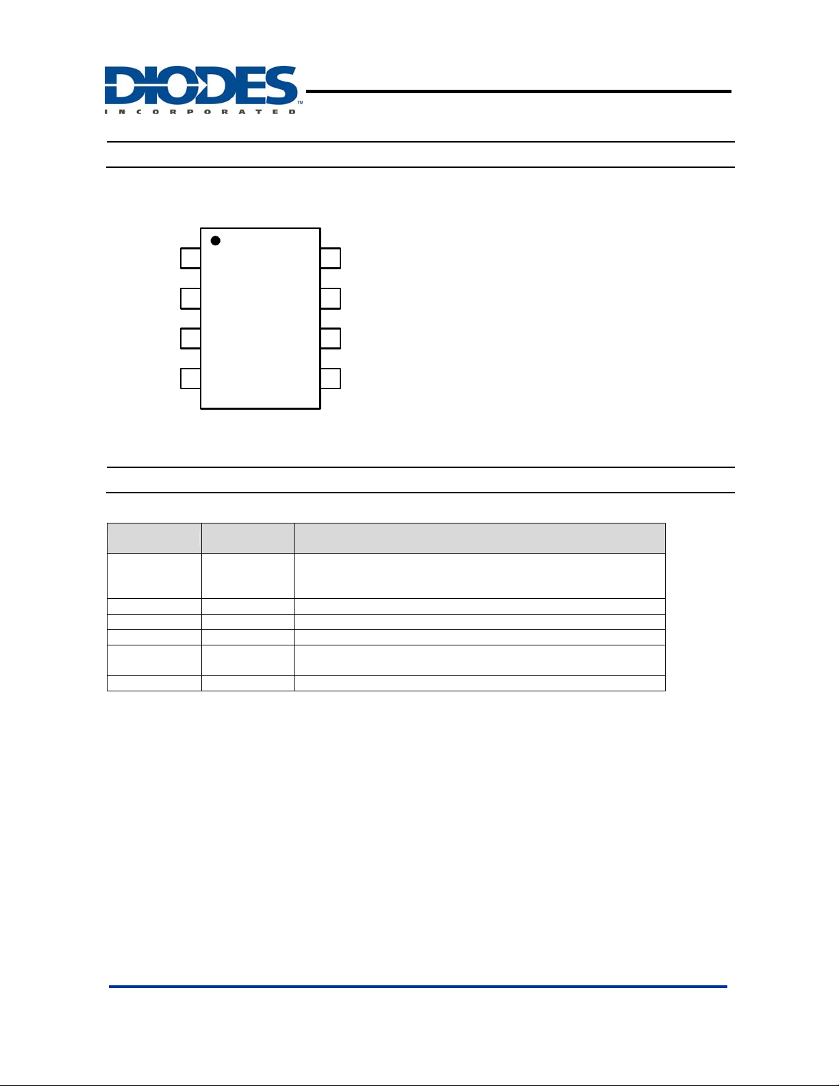
Pin Assignments
( Top View )
AP1609
PWM/PFM DUAL MODE STEP-UP DC/DC CONVERTER
CE
Vcc
FB
PGND
1
2
3
4
SOP-8L
8
GND
GND
7
LX
6
5
LX
Pin Descriptions
Pin Name Pin Number Description
Chip Enable:
CE 1
Vcc 2 IC signal power supply pin
FB 3 Feedback pin
PGND 4 Power MOSFET GND
LX 5, 6
GND 7, 8 GND Pin
AP1609 Rev. 2 2 of 9 FEBRUARY 2009
H: Enable
L: Disable
Switch Pin. Connect external inductor/diode here. Minimize
trace area at this pin to reduce EMI.
www.diodes.com © Diodes Incorporated
Page 3
Block Diagram
AP1609
PWM/PFM DUAL MODE STEP-UP DC/DC CONVERTER
Vcc
FB
Phase
Compensation
+
+
-
-
CE
Vref with
CE
PWM/PFM
Controller
PWM
Comparator
Ramp Wave
Generator,
OSC
Buffer,
Driver
GND
PGND
Absolute Maximum Ratings
Symbol Parameter Ratings Units
VCC V
VFB FB Pin Voltage -0.3 ~ V
VCE CE Pin Voltage -0.3 ~ V
VSW Switch Voltage (LX to GND) -0.3 ~ 18 V
ILX Switch Current -3 ~ 0.2 A
P
Continuous Total Power Dissipation 1200 mW
D
T
Operating Ambient Temperature -20 ~ +80
OPR
T
Storage Temperature -20 ~ +125
STG
Pin Voltage -0.3 ~ 7 V
IN
+0.3 V
CC
+0.3 V
CC
LX
o
C
o
C
AP1609 Rev. 2 3 of 9 FEBRUARY 2009
www.diodes.com © Diodes Incorporated
Page 4

AP1609
PWM/PFM DUAL MODE STEP-UP DC/DC CONVERTER
Electrical Characteristics
AP1609 ( F
Symbol Parameter Conditions Min Typ. Max Units
VFB FB Voltage 1.20 1.23 1.26 V
VCC Input Voltage 2.5 - 6 V
V
Output Voltage 3.0 - 17 V
OUT
Maximum Switching Output
Current
Drain-Source On-State
Resistance
Quiescent Current No Load, FB = 2V, CE = High - 80 130 μA
R
I
OUT
DS (ON)
I
CCQ
ISD Shutdown Current No Load, CE = Low - 1 - μA
Fosc Oscillator Frequency
MAXDTY Maximum Duty Ratio 80 - - %
PFMDTY PFM Duty Ratio No Load 15 25 35 %
V
CE “High” Voltage
CEH
V
CE “Low” Voltage Same as V
CEL
EFFI Efficiency - 91 - %
AP1609 Rev. 2 4 of 9 FEBRUARY 2009
OSC =
300kHz, V
= 5V ) TA = 25 oC
OUT
2.4 - - A
ID = 2.4A - 100 - mΩ
Measuring of EXT Waveform,
V
= Output Voltage +0.3V
IN
240 300 360 kHz
No External Components,
V
= 0V,
FB
Apply 0.65V
(min.) to CE,
CC
0.65 - - *V
Chip Enable
, Chip Disable - - 0.20 *VCC
CEH
www.diodes.com © Diodes Incorporated
CC
Page 5

Typical Application Circuit
(1) Normal Circuit
2.5V~6V
100
330K
100u
3.3u0.1u
0.1u
V
out
AP1609
PWM/PFM DUAL MODE STEP-UP DC/DC CONVERTER
CC
CE
GND
= 1.23
10uH
PGND
R
×
(1+ )
R
LX V
FB
1
, R
2
SS340
= 10K~100K
2
R
R
1
2
C
BP
Option
Vout
0.1u 100u
(2) HV Circuit
above 5.5V
470u
0.1u
ZD
5V
10uH
SS340
15V
R
R
1
C
BP
Option
330K
CE
CC
LX V
FB
0.1u 470u
3.3u
0.1u
V
out
GND
= 1.23
PGND
R
1
×
(1+ )
R
2
= 10K~100K
, R
2
R
2
AP1609 Rev. 2 5 of 9 FEBRUARY 2009
www.diodes.com © Diodes Incorporated
Page 6

)
)
g
(
)
y
y
PWM/PFM DUAL MODE STEP-UP DC/DC CONVERTER
Typical Performance Characteristics
210
180
150
120
90
60
30
Supply Current (uA
0
0.8
0.6
%
0.4
0.2
ulation
-0.2
-0.4
-0.6
Line Re
-0.8
-1
Vc c v s . Su pp ly Curr e n t
V
=Vcc
CE
33.544.555.56
Vcc ( V
1
0
33.544.555.56
Line Regulation
Load = 50mA
Vcc (V)
400
350
300
250
200
150
Frequency (KHz)
100
3 3.5 4 4.5 5 5.5 6
2
1.5
1
0.5
0
-0.5
-1
Load Regulation (%)
-1.5
-2
0 200 400 600 800 1000
AP1609
Vcc vs. Frequency
Load = 300mA
Vcc (V)
Load Regulation
Vcc = 5V
Load (mA)
100
Load vs. Efficienc
95
90
85
80
75
70
Efficiency
65
60
0 0.2 0.4 0.6 0.8 1 1.2 1.4
Vcc = 3.3V,Vout = 5V
Load (A)
100
95
90
85
80
75
Efficiency
70
65
60
0 0.2 0.4 0.6 0.8 1 1.2 1.4
Load vs. Efficienc
Vcc = 5V,Vout = 12V
Load (A)
AP1609 Rev. 2 6 of 9 FEBRUARY 2009
www.diodes.com © Diodes Incorporated
Page 7

PWM/PFM DUAL MODE STEP-UP DC/DC CONVERTER
Typical Performance Characteristics (Continued)
Temperature vs. Freque ncy
400
350
300
250
200
150
Frequency (KHz)
100
-50 -25 0 25 50 75 100
Temperature (oC)
Load = 300mA
Vcc = 5V
Temperature vs. V out
5
4
3
2
1
0
-1
-2
Vout / Vout (%)
-3
-4
-5
-50 -25 0 25 50 75 100
Vcc = 5V
Load = 100mA
Temperature (oC)
Temperature vs. Supply Current
200
180
160
140
120
100
80
60
40
Supply Current (uA)
20
0
-50 -25 0 25 50 75 100
AP1609
Vcc = 5V
Temperature (oC)
AP1609 Rev. 2 7 of 9 FEBRUARY 2009
www.diodes.com © Diodes Incorporated
Page 8

Marking Information
(1) SOP-8L
AP1609
PWM/PFM DUAL MODE STEP-UP DC/DC CONVERTER
( Top View )
8
5
Logo
Part Number
AP1609
WW X
YY
X
41
Package Information (All Dimensions in mm)
(1) Package Type: SOP-8L
0.254
0.62/0.82
7°~9°
Gauge Plane
Seating Plane
Detail "A"
0°/8°
7°~9°
1.27typ
4.85/4.95
0.3/0.5
3.85/3.95
1.30/1.50
5.90/6.10
1.75max.
0.10/0.20
0.15/0.25
Detail "A"
0.35max.
45°
L : Lead Free
G : Green
: Year : 08, 09,10~
YY
WW : Week : 01~52; 52
represents 52 and 53 week
X
: Internal Code
8x-0.60
5.4
6x-1.27
8x-1.55
Land Pattern Recommendation
(Unit: mm)
AP1609 Rev. 2 8 of 9 FEBRUARY 2009
www.diodes.com © Diodes Incorporated
Page 9

AP1609
PWM/PFM DUAL MODE STEP-UP DC/DC CONVERTER
IMPORTANT NOTICE
Diodes Incorporated and its subsidiaries reserve the right to make modifications, enhancements, improvements, corrections or other changes without further
notice to any product herein. Diodes Incorporated does not assume any liability arising out of the application or use of any product described herein; neither
does it convey any license under its patent rights, nor the rights of others. The user of products in such applications shall assume all risks of such use and will
agree to hold Diodes Incorporated and all the companies whose products are represented on our website, harmless against all damages.
LIFE SUPPORT
Diodes Incorporated products are not authorized for use as critical components in life support devices or systems without the expressed written approval of the
President of Diodes Incorporated.
AP1609 Rev. 2 9 of 9 FEBRUARY 2009
www.diodes.com © Diodes Incorporated
 Loading...