Diodes AP1534 User Manual

PWM CONTROL 2A STEP-DOWN CONVERTER
Description
AP1534 consists of step-down switching regulator with PWM
control. These devices include a reference voltage source,
oscillation circuit, error amplifier, internal PMOS.
AP1534 provides low-ripple power, high efficiency, and
excellent transient characteristics. The PWM control circuit is
able to vary the duty ratio linearly from 0 up to 99%. This
converter also contains an error amplifier circuit as well as a
soft-start circuit that prevents overshoot at startup. An
enable function, an over current protect function and a short
circuit protect function are built inside, and when OCP or
SCP happens, the operation frequency will be reduced from
300KHz to 50KHz. Also, an internal compensation block is
built in to minimize external component count.
With the addition of an internal P-channel Power MOS, a
coil, capacitors, and a diode connected externally, these ICs
can function as step-down switching regulators. They serve
as ideal power supply units for portable devices when
coupled with the SO-8 mini-packages, providing such
outstanding features as low current consumption. Since this
converter can accommodate an input voltage up to 18V, it is
also suitable for the operation via an AC adapter.
Pin Assignments
1
FB
2
EN
OCSET
3
V
4
CC
(Top View)
AP1534
SO-8
AP1534
V
8
SS
V
7
SS
Output
6
Output
5
Features
• Input voltage: 3.6V to 18V
• Output voltage: 0.8V to V
• Duty ratio: 0% to 99% PWM control
• Oscillation frequency: 300KHz typical
• Current limit, Enable function
• Thermal Shutdown function
• Built-in internal SW P-channel MOS
• SO-8: Available in “Green” Molding Compound
(No Br, Sb)
• Lead Free Finish/RoHS Compliant (Note 1)
Notes: 1. EU Directive 2002/95/EC (RoHS). All applicable RoHS exemptions applied. Please visit our website at
http://www.diodes.com/products/lead_free.html.
CC
Applications
• PC Motherboard
• LCD Monitor
• Graphic Card
• DVD-Video Player
• Telecom Equipment
• ADSL Modem
• Printer and other Peripheral Equipment
• Microprocessor Core Supply
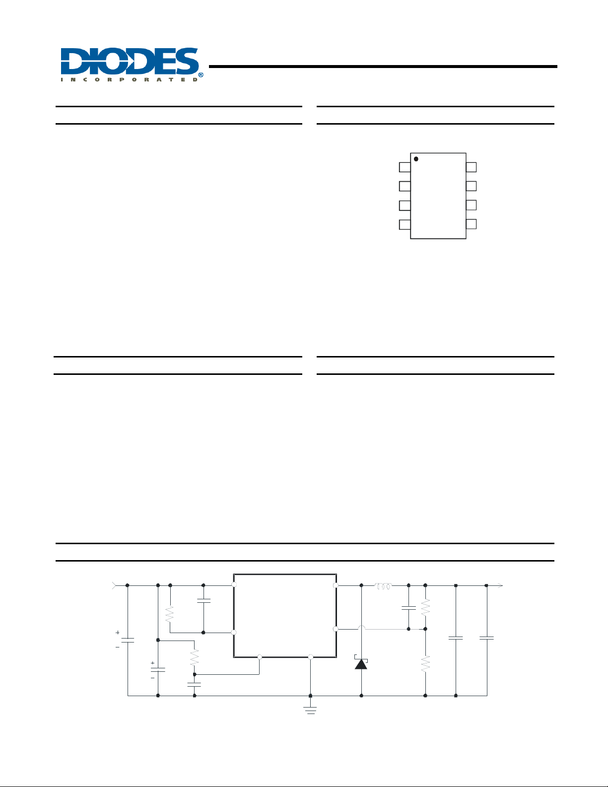
Typical Application Circuit
OCSET
Vcc
OCSET
EN
AP1534
Output
FB
V
SS
V
IN
C
IN
470uF
R
5.6K
CVcc
0.1uF
OCSET
C
Option
R
EN
100K
C
EN
0.1uF
22uH
L1
C
Optional
D1
B240A
(Note 2)
C
R
A
6.8K
R
B
1.3K
V
OUT
+
-
+
C
0.1uF 470uF
-
=5V/2A
C
OUT
Notes: 2. Suggested DIODES Power Schottky P/N: B240/B340 series.
AP1534
Document number: DS31314 Rev. 6 - 2
www.diodes.com
1 of 9
Note: V = V x (1+R /R )
R = 0.7K~5K
OUT FB A B
B
Ω
April 2011
© Diodes Incorporated

PWM CONTROL 2A STEP-DOWN CONVERTER
Pin Descriptions
Pin Name Pin No. Description
FB 1 Feedback pin
Power-off pin
H: Normal operation
EN 2
(Step-down operation)
L: Step-down operation stopped
(All circuits deactivated)
OCSET 3 Add an external resistor to set max output current
VCC
Output 5, 6
VSS
4 IC power supply pin
Switch Pin. Connect external inductor/diode here.
Minimize trace area at this pin to reduce EMI
7, 8 GND Pin
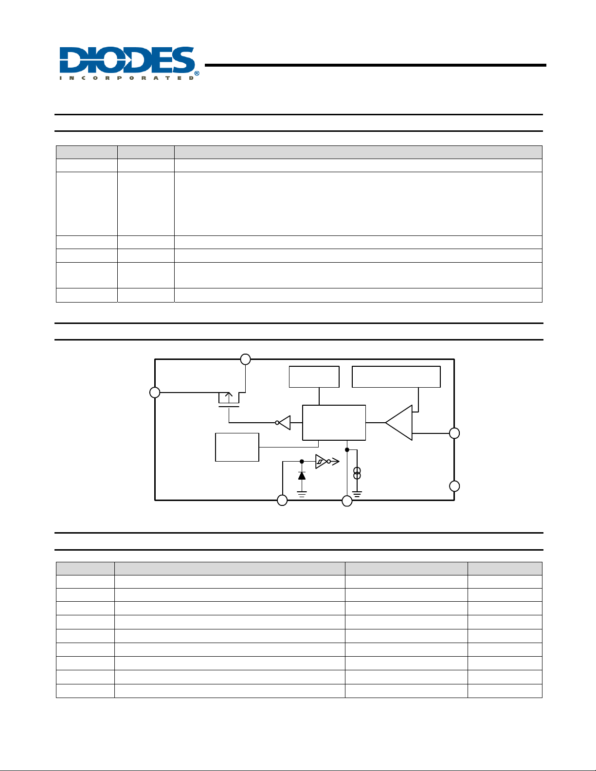
Functional Block Diagram
AP1534
Output
Oscillation
Circuit
Vcc
PWM-Switched
Control Circuit
Thermal
Shutdown
EN
EN
Reference Voltage
Source
100uA
OCSET
+
FB
-
VssV
Absolute Maximum Ratings
Symbol Parameter Rating Unit
ESD HBM Human Body Model ESD Protection 4.5 KV
ESD MM Machine Model ESD Protection 150 V
VCC
VFB
VEN
V
OUT
PD
TJ
T
ST
Caution: The absolute maximum ratings are rated values exceeding which the product could suffer physical damage.
These values must therefore not be exceeded under any conditions.
VCC Pin Voltage
Feedback Pin Voltage
EN Pin Voltage
Switch Pin Voltage
Power Dissipation Internally limited mW
Operating Junction Temperature Range -40 to +125
Storage Temperature Range -65 to +150
AP1534
Document number: DS31314 Rev. 6 - 2
2 of 9
www.diodes.com
VSS - 0.3 to VSS + 20
VSS - 0.3 to VCC
VSS - 0.3 to VIN
VSS - 1.0 to VIN
© Diodes Incorporated
V
V
V
V
o
C
o
C
April 2011

AP1534
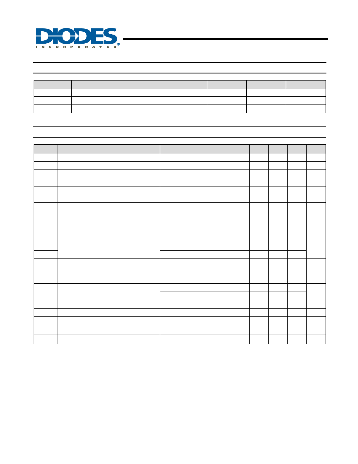
Recommended Operating Conditions
Symbol Parameter Min Max Unit
VIN
I
OUT
TA
Electrical Characteristics (V
Symbol Parameter Conditions Min Typ. Max Unit
VFB
IFB
ISW
I
SHDN
∆V
OUT
/ VIN
∆V
OUT
/V
OUT
f
OSC
f
OSC1
VIH
VIL
ISH
ISL
I
OCSET
R
Notes: 3. Test condition for SO-8: Device mounted on FR-4 substrate PC board, 2oz copper, with minimum recommended pad layout.
For better thermal performance, larger copper pad for heatsink is needed.
Internal MOSFET R
DS(ON)
EFFI Efficiency
T
SHDN
T
HYS
θ
JA
θ
JC
Input Voltage 3.6 18 V
Output Current 0 2 A
Operating Ambient Temperature -20 85
= 12V, TA = 25°C, unless otherwise specified)
IN
Feedback Voltage
Feedback Bias Current
Switch Current -- 2.0 - - A
Current Consumption During Power Off
Line Regulation
Load Regulation
Oscillation Frequency Measure waveform at SW pin 240 300 400 KHz
Frequency of Current Limit or Short Circuit
Protect
EN Pin Input Voltage
EN Pin Input Leakage Current
OCSET Pin Bias Current -- 75 90 105 µA
DS(ON)
Thermal shutdown threshold - 150 - °C
Thermal shutdown hysteresis - 55 - °C
Thermal Resistance Junction-to-Ambient SO-8 (Note 3) - 127 Thermal Resistance Junction-to-Case SO-8 (Note 3) - 28 -
PWM CONTROL 2A STEP-DOWN CONVERTER
o
C
I
= 0.1A
OUT
I
= 0.1A
OUT
V
= 0V
EN
V
= 5V~18V
IN
I
= 0.1 to 2A
OUT
Measure waveform at SW pin - 50 - KHz
Evaluate oscillation at SW pin 2.0 - -
Evaluate oscillation stop at SW pin - - 0.8
-- - 20 - µA
-- - -10 - µA
V
IN
V
IN
V
IN
= 5V, V
= 12V, V
= 12V, V
FB
= 0V
FB
OUT
= 0V
= 5V, I
OUT
= 2A
0.784 0.8 0.816 V
- 0.1 0.5 µA
- 10 - µA
- 1 2 %
- 0.2 0.5 %
- 160 -
- 100 -
- 91 - %
o
o
V
mΩ
C/W
C/W
AP1534
Document number: DS31314 Rev. 6 - 2
3 of 9
www.diodes.com
April 2011
© Diodes Incorporated
 Loading...