Diodes AP1510 User Manual

AP1510
PWM CONTROL 3A STEP-DOWN CONVERTER
Features
• Input voltage: 3.6V to 23V
• Output voltage: 0.8V to V
• Duty ratio: 0% to 100% PWM control
• Oscillation frequency: 300kHz typ.
• Current Limit, Enable function
• Thermal Shutdown function
• Built-in internal SW P-channel MOS
• SOP-8L Pb-Free Package
• SOP-8L: Available in “Green” Molding Compound
(No Br, Sb)
• Lead Free Finish/ RoHS Compliant (Note 1)
.
CC
Applications
• Cellular Phones
• PC Motherboard
• LCD Monitor
• Graphic Card
• DVD-Video Player
• Telecom Equipment
• ADSL Modem
• Printer and other Peripheral Equipment
• Microprocessor core supply
• Networking power supply
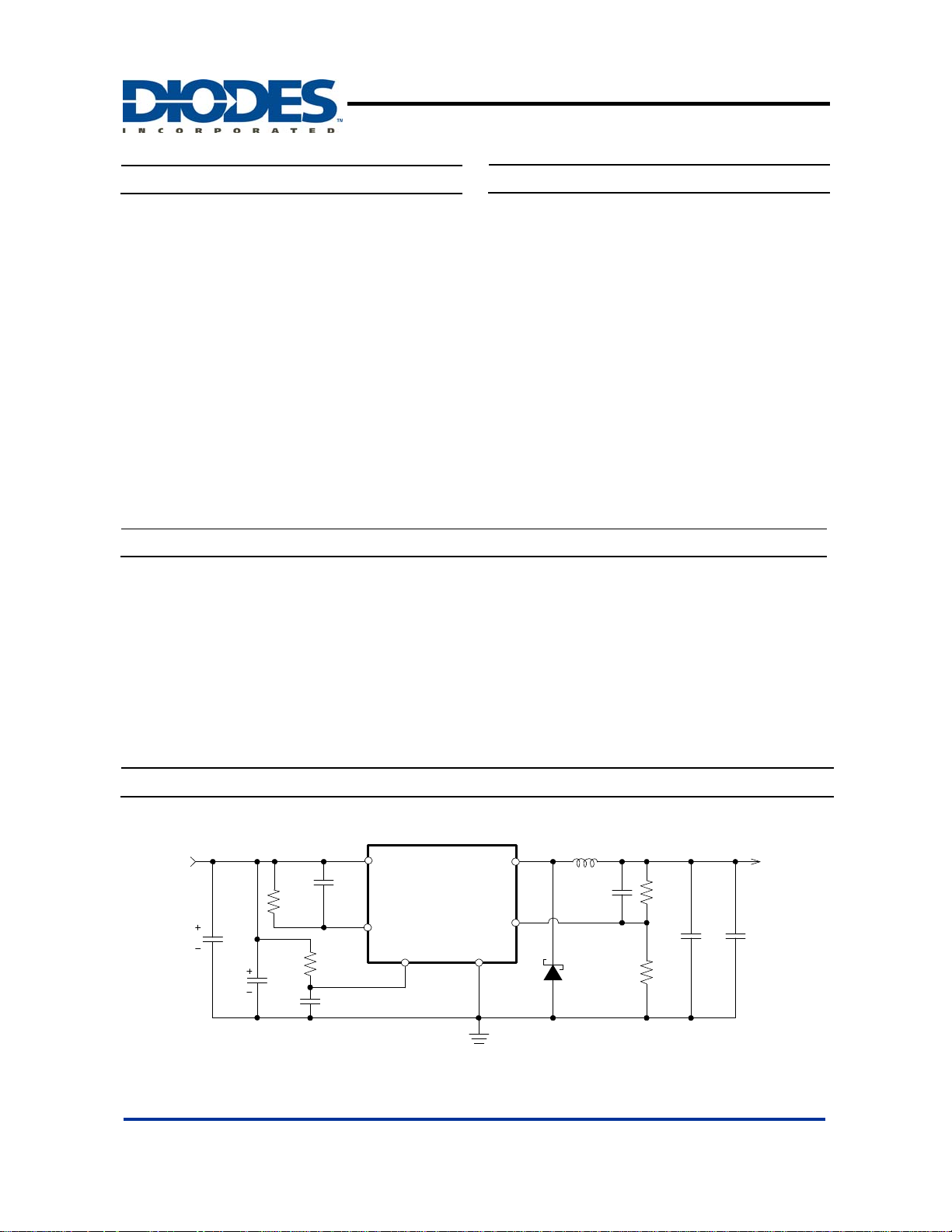
Typical Application Circuit
V
IN
C
IN
470uF
R
3.9K
CVcc
0.1uF
OCSET
C
Option
R
EN
100K
C
EN
0.1uF
OCSET
Vcc
OCSET
EN
AP1510
General Description
AP1510 consists of step-down switching regulator with PWM
control. These devices include a reference voltage source,
oscillation circuit, error amplifier and internal PMOS.
AP1510 provides low-ripple power, high efficiency and excellent
transient characteristics. The PWM control circuit is able to vary
the duty ratio linearly from 0 up to 100%. This converter also
contains an error amplifier circuit. An enable function, an over
current protection and a short circuit protection are built inside,
when OCP or SCP happens, the operation frequency will be
reduced from 300kHz to 30kHz. Also, an internal compensation
block is built in to minimum external component count.
With the addition of an internal P-channel Power MOS, a coil,
capacitors, and a diode connected externally, these ICs can
function as step-down switching regulators. They serve as ideal
power supply units for portable devices when coupled with the
SOP-8L package, providing such outstanding features as low
current consumption. Since this converter can accommodate an
input voltage up to 23V, it is also suitable for the operation via an
AC adapter.
V
=5V/3A
Output
FB
V
SS
L1
22uH
C
Optional
D1
R
C
A
6.8K
R
B
1.3K
OUT
+
+
C
0.1uF 470uF
-
-
C
OUT
Note: V
R
= VFB x (1+RA/RB)
OUT
=0.7K~5K ohm
B
AP1510 Rev. 7 1 of 9 JULY 2009
DS31018 www.diodes.com © Diodes Incorporated

Ordering Information
PWM CONTROL 3A STEP-DOWN CONVERTER
AP1510 S X - 13
AP1510
Package Packing
Device
AP1510SL-13 S SOP-8L 2500/Tape & Reel -13
Lead-free
AP1510SG-13 S SOP-8L 2500/Tape & Reel -13
Notes: 1. EU Directive 2002/95/EC (RoHS). All applicable RoHS exemptions applied. Please visit our website at
http://www.diodes.com/datasheets/ap02001.pdf.
http://www.diodes.com/products/lead_free.html
2. Pad layout as shown on Diodes Inc. suggested pad layout document AP02001, which can be found on our website at
Package
Code
Packaging
(Note 2)
Lead Free
L : Lead Free
G : Green
13 : Tape & ReelS : SOP-8L
13” Tape and Reel
Quantity Part Number Suffix
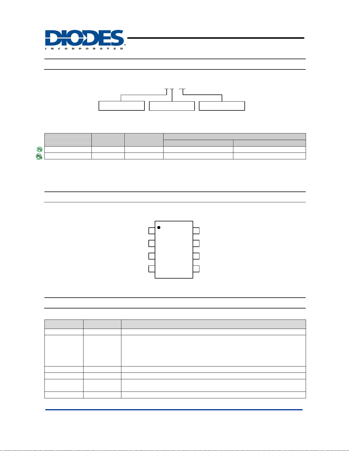
Pin Assignments
( Top View )
FB
EN
OCSET
CC
V
1
2
AP1510
3
4
8
7
6
5
Vss
Vss
Output
Output
SOP-8L
Pin Descriptions
Pin Name Pin NO. Description
FB 1 Feedback pin.
Enable Input pin
H: Normal operation
EN 2
OCSET 3 Add an external resistor to set max output current.
VCC 4 IC power supply pin
Output 5, 6
VSS 7, 8 GND Pin
AP1510 Rev. 7 2 of 9 JULY 2009
DS31018 www.diodes.com © Diodes Incorporated
(Step-down operation)
L: Step-down operation stopped
(All circuits deactivated)
Switch Pin. Connect external inductor/diode here. Minimize trace area at this
pin to reduce EMI.

y
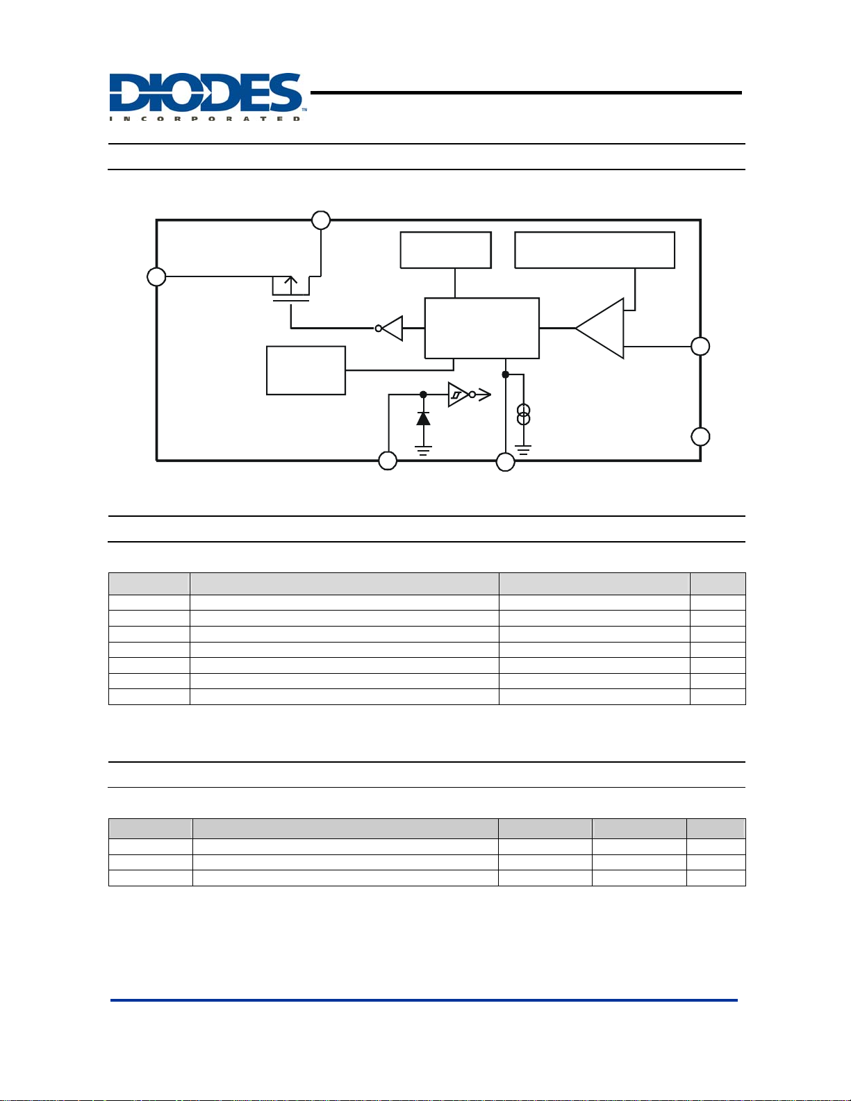
Block Diagram
AP1510
PWM CONTROL 3A STEP-DOWN CONVERTER
Output
Oscillation
Circuit
Reference Voltage
Source with Soft Start
Vcc
PWM-Switched
Control Circuit
+
FB
-
Thermal
Shutdown
EN
EN
100uA
OCSET
VssV
Absolute Maximum Ratings
Symbol Parameter Rating Unit
V
V
CC
V
Feedback Pin Voltage V
FB
V
EN Pin Voltage V
EN
V
Switch Pin Voltage VSS - 0.3 to VIN + 0.3 V
OUT
P
Power Dissipation Internall
D
T
Operating Junction Temperature Range -20 to +125
OP
T
Storage Temperature Range -65 to +150
ST
Caution: The absolute maximum ratings are rated values exceeding which the product could suffer physical damage. These values must therefore not be
exceeded under any conditions.
Pin Voltage VSS - 0.3 to VSS + 25 V
CC
- 0.3 to VCC V
SS
- 0.3 to VIN + 0.3 V
SS
limited mW
o
C
o
C
Recommended Operating Conditions
Symbol Parameter Min Max Unit
VIN Input Voltage 3.6 23 V
I
Output Current 0 3 A
OUT
TA Operating Ambient Temperature -25 85
o
C
AP1510 Rev. 7 3 of 9 JULY 2009
DS31018 www.diodes.com © Diodes Incorporated
 Loading...