

Page 1
AP1501
150KHz, 3A PWM BUCK DC/DC CONVERT ER
Features
• Output voltage: 3.3V, 5V, 12V and adjustable output
version
• Adjustable version output vo l tag e range, 1.23V to
• 150KHZ +
• Voltage mode non-synchronous PWM control
• Thermal-shutdown and current-limit protection
• ON/OFF shutdown control input
• Operating voltage can be up to 40V
• Output load current: 3A
• Low power standb y mode
• Built-in switching transistor on chip
• Lead Free packages: TO263-5L and TO220-5L(R)
• TO263-5L and TO220-5L(R): Available in “Green”
• Lead Free Finish/RoHS Compliant (Note 1)
4%
37V+
Molding Compound (No Br, Sb)
15% fixed switching frequency
Applications
• Simple High-efficiency step-down regulator
• On-card switching regulators
• Positive to negative converter
General Description
The AP1501 is a fully integrated step-down DC/DC converter,
with the ability to drive 3A load without the need of additional
driver components. The AP1501 operates at a switching
frequency of 150KHZ enabling the use of small size filter
components. As a result, board space is reduced and BOM costs
are lowered.
The AP1501 has integrated the shutdown function that allows
standby mode to be activated via an external logic signal input.
The internal compensation facilitates feedback control for line
and load regulation without the need of an external circuitry. The
AP1501 has a built-in Thermal shutdown and Current Limit
function to prevent damage from high operating temperature and
high current operating to the output switch.
Additional features include a guaranteed +/- 4% tolerance on the
output voltage under specified input and output load conditions,
and +/- 15% on oscillator frequency. The AP1501 offers both
fixed and a Adjustable output voltages. For fixed outputs the
AP1501 supports 3.3V, 5.0V and 12V. The package options
available are standard 5-lead TO263 and TO220(R) packages.
Ordering Information
AP1501 - XX
Output version
Blank : Adjustable
33 : 3.3V
50 : 5.0V
Package
K5 : TO263-5L
T5 : TO220-5L
T5R : TO220-5L(R)
12 : 12V
Device
Lead-free
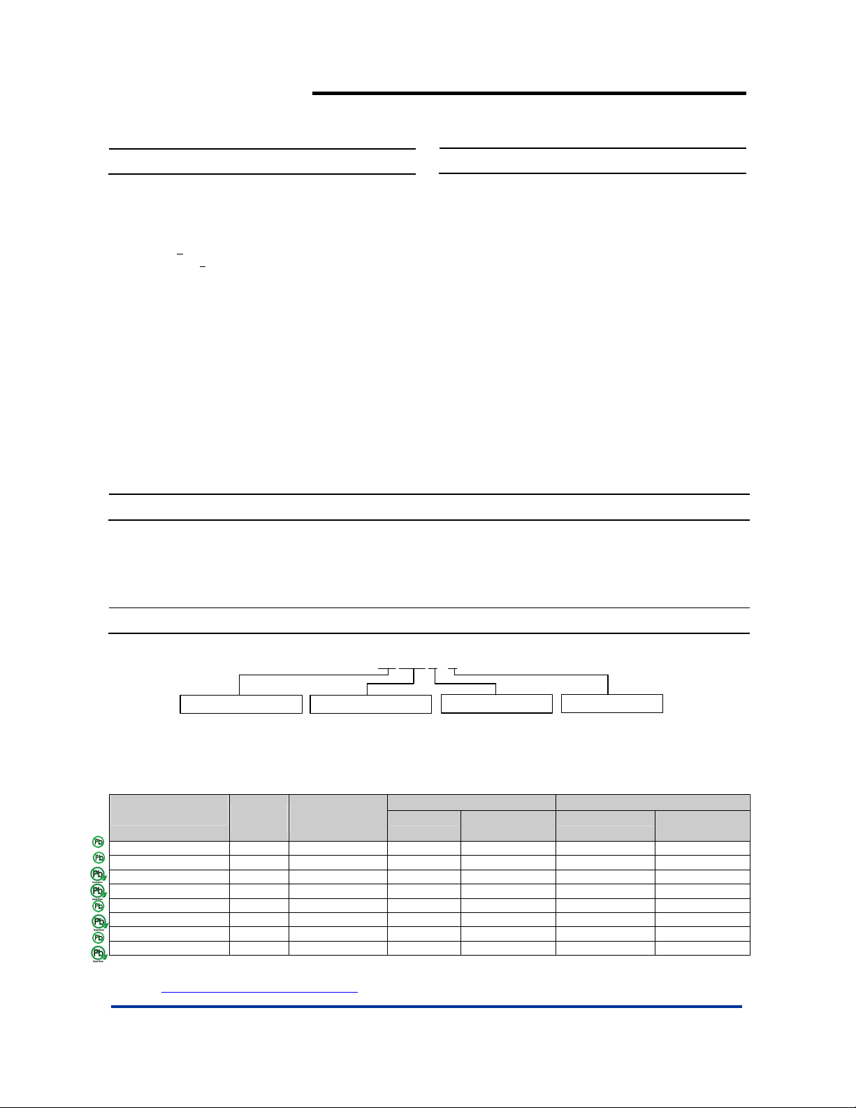
AP1501-XXK5L-U K5 TO263-5L 50 -U NA NA
Lead-free
AP1501-XXK5L-13 K5 TO263-5L NA NA 800/Tape & Reel -13
AP1501-XXK5G-U K5 TO263-5L 50 -U NA NA
AP1501-XXK5G-13 K5 TO263-5L NA NA 800/Tape & Reel -13
AP1501-XXT5L-U T5 TO220-5L 50 -U NA NA
Lead-free
AP1501-XXT5G-U T5 TO220-5L 50 -U NA NA
AP1501-XXT5RL-U T5R TO220-5L(R) 50 -U NA NA
Lead-free
AP1501-XXT5RG-U T5R TO220-5L(R) 50 -U NA NA
Notes: 1. EU Directive 2002/95/EC (RoHS). All applicable RoHS exemptions applied, see EU Directive 2002/95/EC Annex Notes.
2. Pad layout as shown on Diodes Inc. suggested pad layout document AP02001, which can be found on our website at
http://www.diodes.com/datasheets/ap02001.pdf.
Package
Code
Packaging
(Note 2)
AP1501 Rev. 11 1 of 12 JANUARY 2009
XXX X - X
Lead Free
L : Lead Free
G : Green
Packing
U : Tube
13 : Tape & Reel
Tube 13” Tape and Reel
Quantity Part Number
Suffix
.
Quantity Part Number
Suffix
www.diodes.com © Diodes Incorporated
Page 2
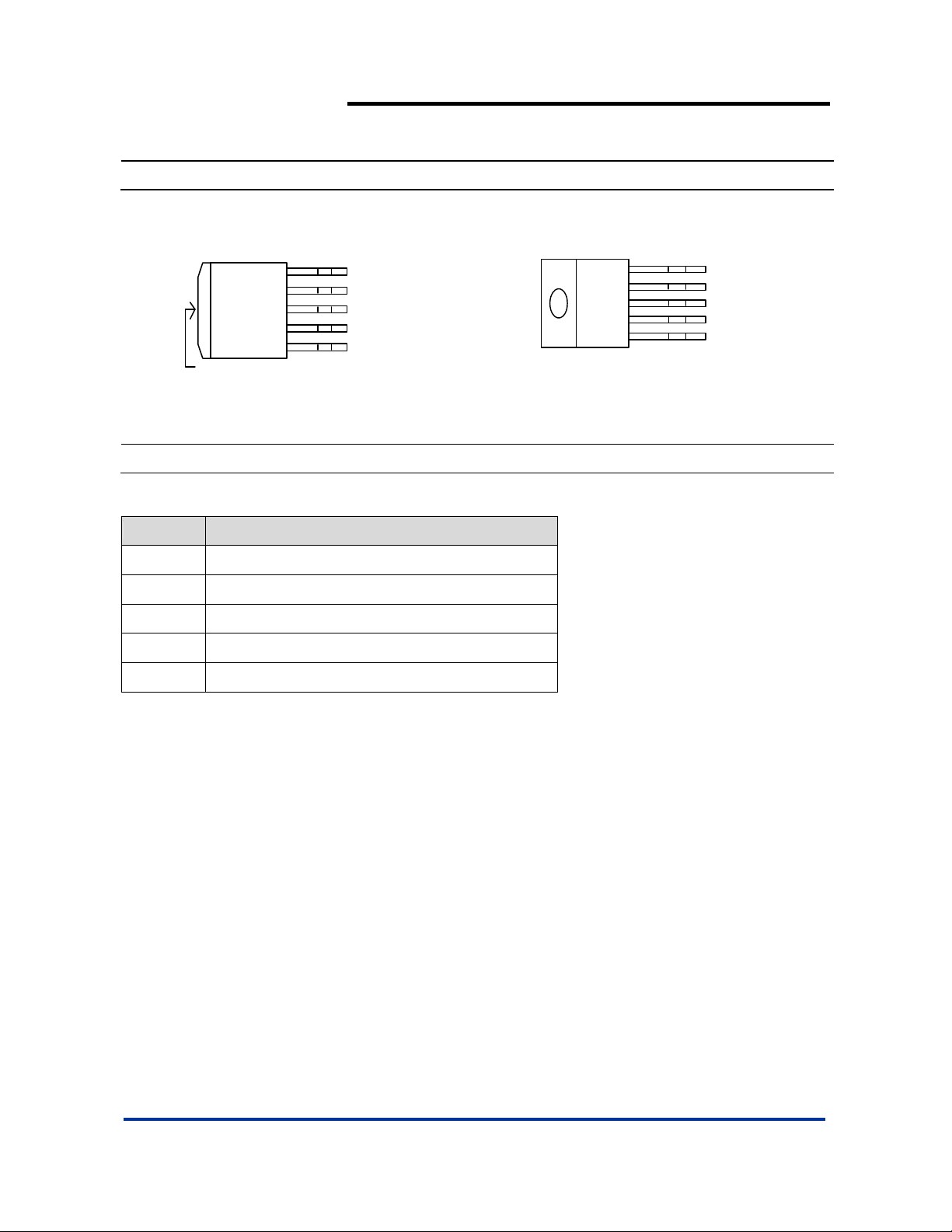
Pin Assignments
( Top View )
AP1501
150KHz, 3A PWM BUCK DC/DC CONVERT ER
( Top View )
5 SD
4 FB
3 Gnd
2 Output
1 V
Metal Tab GND
TO263-5L
Pin Descriptions
Name Description
VIN Operating voltage input
Output Switching output
Gnd Ground
FB Output voltage feedback control
SD ON/OFF shutdown
5 SD
4 FB
3 Gnd
2 Output
1 V
IN
TO220-5L/TO220-5L(R)
IN
AP1501 Rev. 11 2 of 12 JANUARY 2009
www.diodes.com © Diodes Incorporated
Page 3
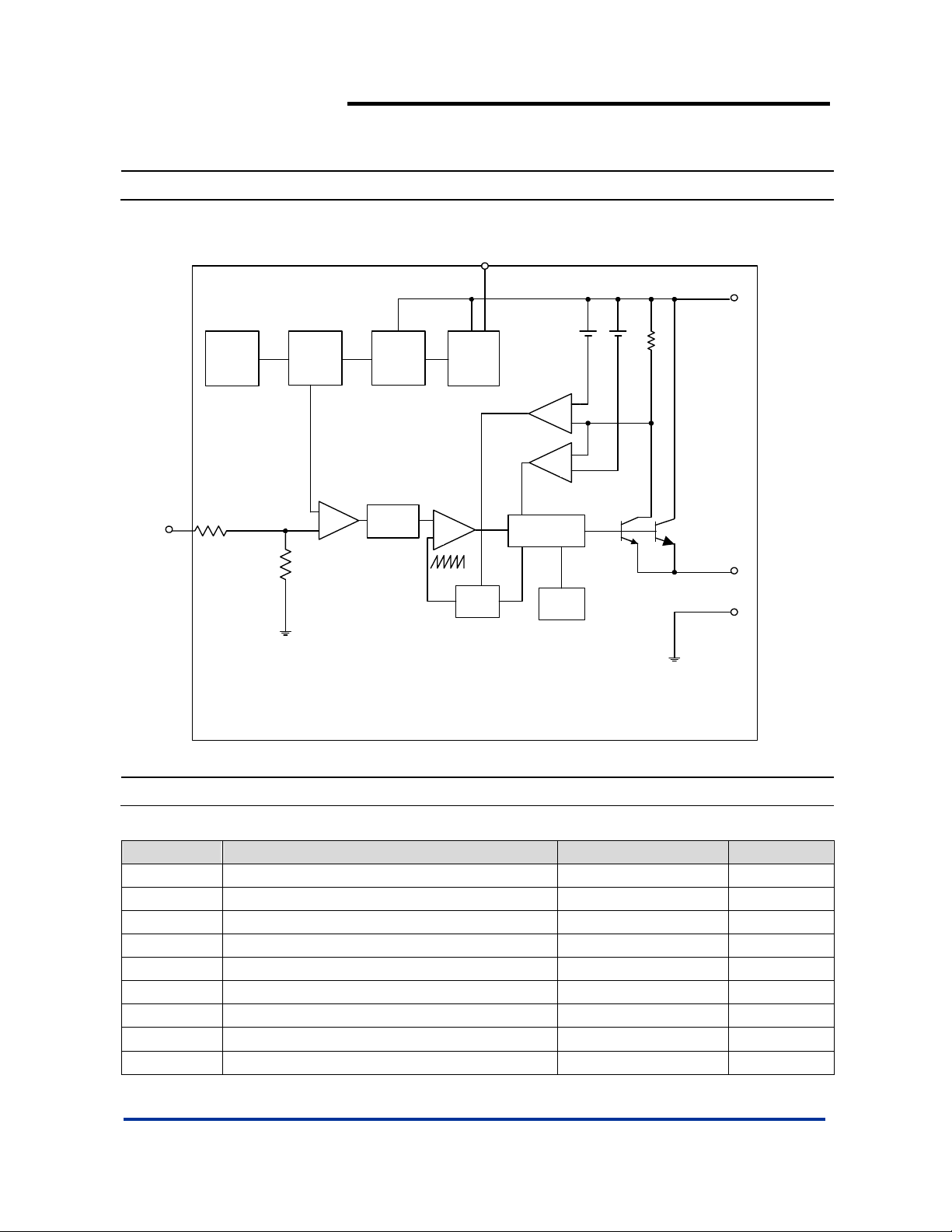
Block Diagram
Current
Source
bias
1.235V
Reference
2.5V
Regulator
AP1501
150KHz, 3A PWM BUCK DC/DC CONVERT ER
SD
V
IN
220mV200mV
Start
up
+
Comp
_
_
Comp
+
FB
+
_
Amp
Frequency
compen-
sation
_
Comp
+
150kHz
OSC.
Pre-driver
Thermal
Shutdown
3A
Switch
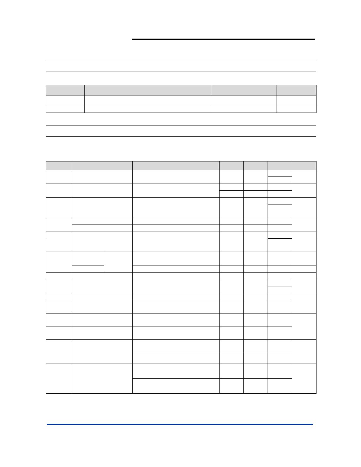
Absolute Maximum Ratings
Symbol Parameter Rating Unit
ESD MM Machine Model ESD Protection 400 V
VCC Supply Voltage +45 V
VSD ON/OFF Pin input Voltage -0.3 to +40 V
VFB Feedback Pin Voltage -0.3 to +40 V
V
Output Voltage to Ground -1 V
OUT
PD Power Dissipation Internally limited W
TST Storage Temperature -65 to +150
TJ Operating Junction Temperature -20 to +125
T
MJ
Maximum Junction Temperature 150
Output
Gnd
o
C
o
C
oC
AP1501 Rev. 11 3 of 12 JANUARY 2009
www.diodes.com © Diodes Incorporated
Page 4
f
(reg
)
AP1501
150KHz, 3A PWM BUCK DC/DC CONVERT ER
Recommended Operating Conditions
Symbol Parameter
Rating
VOP Operating Voltage 4.5 to 40 V
TA Oper at i n g Am bi ent Temperatur e -20 to 85
Electrical Characteristics (All Output Voltage Versions)
Unless otherwise specified, V
Specifications with boldface type are for full operating temperature range, the other type are for T
Symbol Parameter Conditions Min Typ. Max Unit
IFB Feedback Bias Current
F
Oscillator Frequency
OSC
V
Saturation Voltage
SAT
DC
Max. Duty Cycle(ON)
Min. Duty cycle(OFF)
ICL Current Limit
Output = 0
IL
Output = -1
IQ Quiescent Current
I
STBY
VIH
Standby Quiescent
Current
VIL
ON/OFF pin Logic Input
Threshold Voltage
ON/OFF Pin Logic
IH
Input Current
ON/OFF Pin Input
IL
Current
= 12V for 3.3V, 5V, adjustable version and V
IN
= 1.3V
V
FB
(Adjustable version only)
I
= 3A
OUT
No outside circuit
= 0V force driver on
V
FB
V
= 0V force driver on 100
FB
V
= 12V force driver off 0
FB
Peak current
no outside circuit
= 0V force driver on
V
FB
Output
Leakage
Current
No outside circuit
= 12V force driver off (Note 3)
V
FB
= 40V 2 60
V
IN
= 12V force driver of
V
FB
ON/OFF pin = 5V
= 40V
V
IN
Low
ulator ON
High (regulator OFF) 2.0
= 2.5V (OFF) 15 25
V
LOGIC
= 0.5V (ON) 0.02 5
V
LOGIC
= 24V for the 12V version. I
IN
J
40
127 150 173
110 173
1.3
3.6 4.0
200
150
= 0.5A
LOAD
= 25ºC.
5 10
1.3
60
100
1.4
1.5
5.5
6.5
250
350
0.6
Units
o
C
KHZ
nA
%
uA
mA
mA
uA
uA
V
A
V
θ
θ
Notes: 3 . Feedback pin removed from output and connected to 0V to force the output transistor switch ON. Feedback pin rem oved from output and
Thermal Resistance
JA
unction to Ambient
Thermal Resistance
JC
Junction to Case
connected to 12V for the 3.3V, 5V, and the ADJ. version, and 15V for the 12V version, to force the output transistor switch OFF.
4. Test condition: Device mounted with copper area of approximately 3 in
TO263-5L (Note 4) 37
TO220-5L(R) (Note 4) 31
TO263-5L (Note 4) 6
TO220-5L(R) (Note 4) 5
2
,1oz, no air flow.
o
C/W
o
C/W
AP1501 Rev. 11 4 of 12 JANUARY 2009
www.diodes.com © Diodes Incorporated
Page 5

150KHz, 3A PWM BUCK DC/DC CONVERT ER
Electrical Characteristics (Continued)
Specifications with boldface type are for full operating temperature range, the other type are for TJ = 25ºC.
AP1501-ADJ
AP1501-3.3V
AP1501-5V
AP1501-12V
Symbol Parameter Conditions V
VIN < 40V
V
FB
η
V
OUT
η
V
OUT
η
V
OUT
η
Output
Feedback
Efficiency V
Output Voltage
Efficiency V
Output Voltage
Efficiency V
Output Voltage
Efficiency V
4.5V <
0.2A < I
V
OUT
= 12V, I
IN
4.75V <
0.2A <
= 12V, I
IN
7V <
0.2A <
= 12V, I
IN
15V <
0.2A <
= 15V, I
IN
< 3A
LOAD
programmed for 3V
LOAD
VIN < 40V
I
< 3A
LOAD
LOAD
VIN < 40V
I
< 3A
LOAD
LOAD
VIN < 40V
I
< 3A
LOAD
LOAD
= 3A 73 %
= 3A 73 %
= 3A 80 %
= 3A 90 %
Typ. V
Min
1.193
1.18
1.23
3.168
3.135
4.8
4.75
11.52
11.4
3.3
5
12
AP1501
Unit
Max
1.267
1.28
3.432
3.465
5.2
5.25
12.48
12.6
V
V
V
V
AP1501 Rev. 11 5 of 12 JANUARY 2009
www.diodes.com © Diodes Incorporated
Page 6

s
150KHZ, 3A PWM BUCK DC/DC CONVERTER
Typical Performance Characteristics
Typical Performance Characteristic
Normalized Output Voltage
AP1501
Efficiency
OUTPUT VOLTAGE (V)
SATURATION VOLTAGE (V)
5.10
5.05
5.00
4.95
4.90
-50 -25 0 25 50 75 100 125
JUNCTION TEMPERATURE(oC)
VIN=20V, I
Normalized at T
Switch Saturation Voltage
1.60
1.40
1.20
1.00
0.80
0.60
1 : -40oC
2 : 25
3 : 125
1
2
3
0.5
o
C
o
C
1
SWITCH CURRENT(A)
23
LOAD
=3A
=25oC
J
100
95
90
85
80
EFFICIENCY (%)
75
70
65
5V
3.3V
8101520253035
JUNCTION TEMPERATURE(oC)
3A Load
40
Switch Current Limit
5.50
VIN=12V, V
5.00
4.50
4.00
SWITCH CURRENT LIMIT (A)
3.50
-50 -25 0 25 50 75 100 125
JUNCTION TEMPERATURE(
OUT
=5V
o
C)
Operating Quiescent Current
25.0
20.0
15.0
10.0
5.0
SUPPLY CURRENT (mA)
0.0
-50 -25 0 25 50 75 100 125
JUNCTION TEMPERATURE(oC)
Switch ON
Switch OFF
200.0
160.0
120.0
CURRENT (uA)
Shutdown Quiescent Current
1
2
80.0
40.0
0.0
3
10 20 30 40
SUPPLY VOLOTAGE (V)
V
ON/OFF
1 : -40
2 : 25
3 : 125
o
o
o
=5V
C
C
C
AP1501 Rev. 11 6 of 12 JANUARY 2009
www.diodes.com © Diodes Incorporated
Page 7

150KHz, 3A PWM BUCK DC/DC CONVERT ER
Typical Performance Characteristics (Continued)
Minimum Operating Supply Voltage
5.0
5.0
AP1501
ON/OFF Threshold Voltage
4.0
3.0
2.0
V
1.0
SUPPLY VOLTAGE (V)
0.0
OUT
I
LOAD
-50 -25 0 25 50 75 100 125
JUNCTION TEMPERATURE (oC)
ON/OFF Pin Current (Sinking)
150.0
120.0
90.0
60.0
CURRENT (uA)
30.0
VIN=40V
-40
0.0
1.45 10152022232425
=1.23V
=120mA
o
C TJ 125oC
≤≤
ON/OFF PIN VOLTAGE (V)
4.0
3.0
2.0
1.0
THRESHOLD VOLTAGE (V)
0.0
-50
0
-25
JUNCTION TEMPERATURE (oC)
Switch Frequency
200.0
150.0
100.0
50.0
FREQUENCY (kHz)
0.0
-50 -25 0 25 50 75 100 125
JUNCTION TEMPERATURE (oC)
25 50 75
100 125
Feedback Pin Bias Current
50.0
40.0
30.0
20.0
Adjustable Version Only
BIAS CURRENT (nA)
10.0
0.0
-50 -25 0 25 50 75 100 125
o
JUNCTION TEMPERATURE(
C)
AP1501 Rev. 11 7 of 12 JANUARY 2009
www.diodes.com © Diodes Incorporated
Page 8

×
Typical Application Circuit
(1) Fixed Type Circuit
12V
DC Input
12
Vin
Cin
Capacitor
(2) Adjustable Type Circuit
FB
4
AP1501
-33
SD
R2
35
Gnd
AP1501
150KHz, 3A PWM BUCK DC/DC CONVERT ER
Output
L1
33uH
Inductor
D1
B340A
R1
3.3V/3A
Output Load
Co
Capacitor
12V
DC Input
Cin
Capacitor
(3) Delay Start Circuit
12V
DC Input
Cin
Capacitor
FB
4
12
Vin
AP1501
SD
V
V
= V
out
= 1.23V
FB
R2 = 1K ~ 3K
R2
FB
4
12
AP1501
SD
R
DELAY
10K
C
DELAY
0.1uF
Vin
L1
Output
35
Gnd
47uH
D1
(Note 5)
5V/ 3A
Output Load
Co
Capacitor
R1
(1 +
FB
Output
35
Gnd
R2
)
R1
47uH
D1
(Note 5)
L1
5V/ 3A
Output Load
Co
Capacitor
Notes: 5. Suggested DIODES Power Schottky: B340A or PDS340 series.
AP1501 Rev. 11 8 of 12 JANUARY 2009
www.diodes.com © Diodes Incorporated
Page 9

AP1501
150KHz, 3A PWM BUCK DC/DC CONVERT ER
Functional Description
Pin Functions
+V
IN
This is the positive input supply for the IC switching regulator. A
suitable input bypass capacitor must be present at this pin to
minimize voltage transients and to supply the switching currents
needed by the regulator.
Ground
Circuit ground.
Output
Internal switch. The voltage at this pin switches between (+V
) and approximately – 0.5V, with a duty cycle of
V
SAT
approximately V
circuitry, the PC board copper area connected to this pin should
be kept a minimum.
Feedback
Senses the regulated output voltage to complete the feedback
loop.
ON/OFF
Allows the switching regulator circuit to be shutdown using logic
level signals thus dropping the total input supply current to
approximately 150uA. Pulling this pin below a threshold voltage
of approximately 1.3V turns the regulator on, and pulling this pin
above 1.3V (up to a maximum of 40V) shuts the regulator down.
If this shutdown feature is not needed, the ON/OFF pin can be
wired to the ground pin or it can be left open, in either case the
regulator will be in the ON condition.
Thermal Considerations
The AP1501 is available in 5-pin surface mount TO-263 and
TO-220.
The TO-220 package needs a heat sink under most conditions.
The size of the heat sink depends on the input voltage , the output
voltage, the load current and the ambient temperature. The
AP1501 junction temperature rises above ambient temperature
for a 3A load and different input and output voltages. The data
for these curves was taken with the AP1501 (TO-220 package)
operating as a buck switching regulator in an ambient
temperature of 25
are all approximate and there are many factors that can affect
these temperatures. Higher ambient temperatures require more
heat sinking.
The TO-263 surface mount package tab is designed to be
soldered to the copper on a printed circuit board. The copper
and the board are the heat sink for this package and the other
heat producing components, such as the catch diode and
inductor. The PC board copper area that the package is
soldered to should b e at least 0.4 in
2 or more square inches of 2 oz. Additional cop per area improv es
the thermal characteristics, but with copper areas greater than
approximately 6 in
are realized. If further thermal improvements are needed, double
sided, multilayer PC boards with large copper areas and/or
airflow are recommended.
The AP1501 (TO-263 package) junction temperature rises above
ambient temperature with a 2A load for various input and output
voltages. This data was taken with the circuit operating as a
buck switching regulator with all components mounted on a
/ VIN. To minimize coupling to sensitive
OUT
o
C (still air). These temperature rise numbers
2
, and ideally should have
2
, only small improvements in heat dissipation
IN
AP1501 Rev. 11 9 of 12 JANUARY 2009
www.diodes.com © Diodes Incorporated
PC board to simulate the junction temperature under actual
operating conditions. This curve can be used for a quick check
for the approximate junction temperature for various conditions,
but be aware that there are many factors that can affect the
junction temperature. When load currents higher than 2A are
used, double sided or multilayer PC boards with large copper
areas and/or airflow might be needed, especially for high ambient
temperatures and high output voltages.
For the best thermal performance, wide copper traces and
generous amounts of printed circuit board copper sh ou ld be used
in the board layout. (One exception to this is the output (switch)
–
pin, which should not have large areas of copper.) Large areas
of copper provide the best transfer of heat (lower thermal
resistance) to the surrounding air, and moving air lowers the
thermal resistance even further.
Package thermal resistance and junction temperature rise
numbers are all approximate, and there are many factors that will
affect these numbers. Some of these factors include board size,
shape, thickness, position, location, and even board temperature.
Other factors are, trace width, total printed circuit copper area,
copper thickness, single or double-sided, multilayer board and
the amount of solder on the board. The effectiveness of the
PC board to dissipate heat also depends on the size, quantity
and spacing of other components on the board, as well as
whether the surrounding air is still or moving.
Furthermore, some of these components such as t he catch diode
will add heat to the PC board and the heat can vary as the input
voltage changes. For the inductor, depending on the physical
size, type of core material and the DC resistance, it could either
act as a heat sink taking heat away from the board, or it could
add heat to the board.
Page 10

Marking Information
(1) TO263-5L
AP1501
150KHz, 3A PWM BUCK DC/DC CONVERT ER
( Top View )
Logo
Output Type :
1501 : ADJ
1501-33 : 3.3V
1501-50 : 5.0V
1501-12 : 12V
(2) TO220-5L(R)
Output Type :
1501: ADJ
1501-33: 3.3V
1501-50: 5.0V
1501-12: 12V
1501-XX
YY WW
( Top view )
X
1501-XX
YY WW X X
X
L : Lead Free
G : Green
ID code
Xth week : 01~52
Year :
Logo
L : Lead Free
G : Green
ID code
Xth week : 01~52
Year : "07" = 2007
"07" = 2007
"08" = 2008
~
"08" = 2008
~
AP1501 Rev. 11 10 of 12 JANUARY 2009
www.diodes.com © Diodes Incorporated
Page 11

Package Information
(1) Package Type: TO263-5L
AP1501
150KHz, 3A PWM BUCK DC/DC CONVERT ER
(2) Package Type: TO220-5L
AP1501 Rev. 11 11 of 12 JANUARY 2009
www.diodes.com © Diodes Incorporated
Page 12

150KHz, 3A PWM BUCK DC/DC CONVERT ER
Package Information (Continued)
(3) Package Type: TO220-5L(R) Mechanical drawing
AP1501
IMPORTANT NOTICE
Diodes Incorporated and its subsidiaries reserve the right to make modifications, enhancements, improvements, corrections or other changes without further
notice to any product herein. Diodes Incorporated does not assume any liability arising out of the application or use of any product described herein; neither
does it convey any license under its patent rights, nor the rights of others. The user of products in such applications shall assume all risks of such use and will
agree to hold Diodes Incorporated and all the companies whose products are represented on our website, harmless against all damages.
LIFE SUPPORT
Diodes Incorporated products are not authorized for use as critical components in life support devices or systems without the expressed written approval of the
President of Diodes Incorporated.
AP1501 Rev. 11 12 of 12 JANUARY 2009
www.diodes.com © Diodes Incorporated
 Loading...