

Page 1
AP139
300mA LOW-NOISE CMOS LDO
Features
• Very Low Dropout Voltage
• Low Current Consumption: Typ. 45μA, max. 60uA
• Output Voltage: 1.5V, 1.8V, 2.0V, 2.5V, 2.8V, 3.0V
3.3V, and 3.5V
• Guaranteed 300mA Output
• Input Range from 2.7 up to 5.5V
• Thermal Shutdown
• Current Limiting
• Stability with Low ESR Capacitors
• Low Temperature Coeff icient
• Lead Free Package: SOT25
• SOT25: Available in “Green” Molding Compound
(No Br, Sb)
• Lead Free Finish/RoHS Compliant (Note 1)
Applications
• Personal Communication Devices
• Home Electric/Electronic Appliances
• PC Peripherals
• Battery-Powered Devices
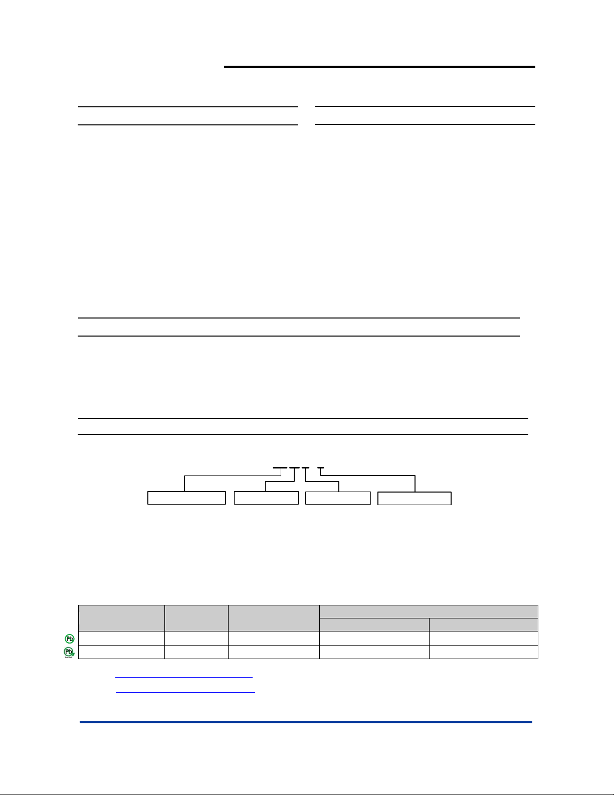
Ordering Information
AP139 - XX W X - 7
General Description
The AP139 is a positive voltage linear regulator utilizing CMOS
technology. The features that include low quiescent current
(45μA typ.), low dropout voltage, and high output voltage
accuracy, make it ideal for battery applications. EN input
connected to the device will produce a low bias current.
The space-saving SOT25 package is attractive for “pocket” and
“hand held” applications.
This rugged device has both thermal shutdown, and current limit
protections to prevent device failure under the “worst” operating
conditions.
In a low noise, regulated supply application, a 10nF capacitor is
necessary to be placed in between Bypass and Ground.
The AP139 is stable with a low E SR out put ca paci tor of 1.0μF or
greater.
Output Voltage
15 :1.5V
18 :1.8V
Package Packing
W : SOT25
Lead Free
L : Lead Free
G : Green
7 : Tape & Reel
20 :2.0V
25 :2.5V
28 :2.8V
30 :3.0V
33 :3.3V
35 :3.5V
Device
AP139-XXWL-7
Lead-free
AP139-XXWG-7
Notes: 1. EU Directive 2002/95/EC (RoHS). All applicable RoHS exemptions applied. Please visit our website at
http://www.diodes.com/products/lead_free.html
2. Pad layout as shown on Diodes Inc. suggested pad layout document AP02001, which can be found on our website at
http://www.diodes.com/datasheets/ap02001.pdf
Package
Code
W SOT25
W SOT25
Packaging
(Note 2)
.
.
Quantity Part Number Suffix
3000/Tape & Reel -7
3000/Tape & Reel -7
7” Tape and Reel
AP139 Rev. 6 1 of 7 FEBRUARY 2009
www.diodes.com © Diodes Incorporated
Page 2
AP139
300mA LOW-NOISE CMOS LDO
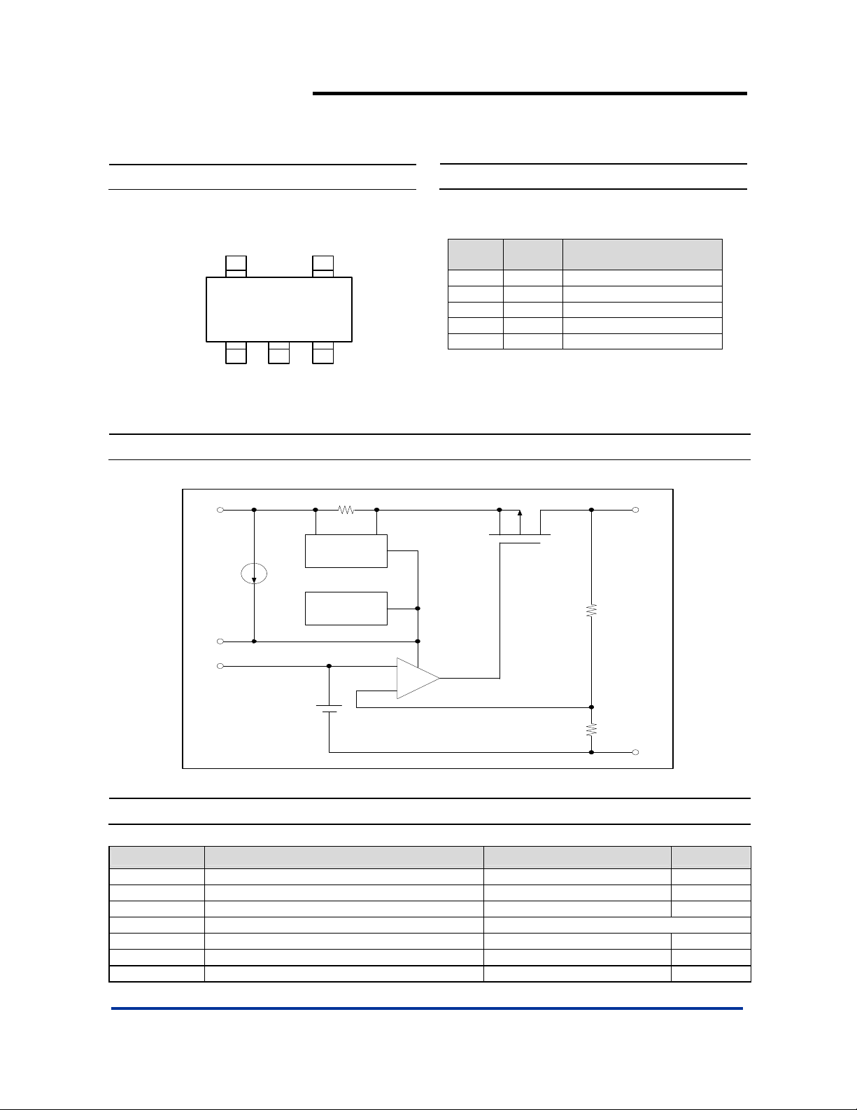
Pin Assignments
( Top View )
V
OUT
5 4
1 32
V
IN
Block Diagram
V
IN
1uA
AP139
GND
SOT25
BYP
EN
Current
Limit
Pin Descriptions
Pin
Name
V
GND 2 Ground
EN 3 Enable Pin
BYP 4 Bypass Signal Pin
V
Pin No. Description
1 Power Supply
IN
5 Output
OUT
V
OUT
BYP
Thermal
Shutdown
EN
-
AMP
+
Vref
R1
R2
GND
Absolute Maximum Ratings
Symbol Parameter Rating Unit
VIN Input Voltage +6 V
I
Output Current PD/(VIN-VO) mA
OUT
V
Output Voltage GND - 0.3 to VIN+ 0.3 V
OUT
ESD Classification B
TOP Operating Junction Temperature Range -40 to +125 ºC
TMJ Maximum Junction Temperature 150 ºC
PD Internal Power Dissipation 250 mW
AP139 Rev. 6 2 of 7 FEBRUARY 2009
www.diodes.com © Diodes Incorporated
Page 3
AP139
300mA LOW-NOISE CMOS LDO
Recommended Operating Conditions
Symbol Parameter Min Max Unit
V
IN
I
OUT
T
A
Electrical Characteristics (T
Symbol Parameter Test Conditions Min Typ. Max Unit
VIN Input Voltage
IQ Quiescent Current IO = 0mA - 45 60 μA
I
Standby Current V
STB
V
OUT
V
DROPOUT
I
Output Current 300 - - mA
OUT
I
Current Limit V
LIMIT
I
Short Circuit Current
short
△V
LINE
△V
LOAD
PSRR Power Supply Rejection
PSRR Power Supply Rejection
VEH
VEL Output OFF - - 0.8 V
IEN Enable Pin Current - - <0.1 μA
OTS
OTH
θ
Thermal Resistance SOT25 (Note 4) 226 ºC/W
JA
θ
Thermal Resistance SOT25 (Note 4) 34 ºC/W
JC
Notes: 3. V
4. Test conditions for SOT25: Devices mounted on FR-4 PC board, MRP, 1 oz. copper, single sided, calibrate at TJ=85 ºC, measure at TA=25 ºC,
no heat Sink, no air flow.
AP139 Rev. 6 3 of 7 FEBRUARY 2009
Input voltage
2.7 5.5 V
Output Current 0 300 mA
Operating Ambient Temperature
Output Voltage Accuracy I
V
Temperature
OUT
Coefficient
Dropout Voltage
Line Regulation I
Load Regulation I
= +25ºC, unless otherwise noted)
A
= 5.0V, V
IN
= 1mA, V
O
= 0V, VEN < VEL - 2.0 3.0 μA
OUT
= 5V -2 - 2 %
IN
- 50 - ppm/
I
= 1mA to 300mA,
O
V
= V
OUT
> 1.05V 300 450 - mA
OUT
V
= 5V, V
cc
= 1mA, V
OUT
= 1mA to 300mA, V
O
I
= 100mA,
O
= 2.2μF ceramic
C
O
= 100mA,
I
O
C
= 2.2μF ceramic,
O
C
= 20nF
BYP
O(NOM)
out
- 1.5%
< 1.05V
= (V
IN
V
+1V) to 5.5V - 0.1 0.3 %
OUT
= 5V - 0.3 1 %
IN
f = 1KHz - 60 f = 10KHz - 50 f = 100KHz - 40 f = 1KHz - 75 f = 10KHz - 55 f = 100KHz - 30 -
-40 85
Note 3
≥2.8V
O
- - 0.45 V
- 150 300 mA
- 5.5 V
Output ON 1.7 - - V
EN Input Threshold
Over Temperature
Shutdown
Over Temperature
Hysteresis
= V
OUT
+ V
DROPOUT.
IN(MIN)
- 130 -
- 20 -
www.diodes.com © Diodes Incorporated
°C
dB
dB
o
C
o
C
o
C
Page 4

Typical Application
IN OUT
300mA LOW-NOISE CMOS LDO
V
IN
AP139
BYP EN
GND
V
OUT
AP139
C1
1uF
C2
10nF
Typical Performance Characteristics
100
90
80
70
60
50
40
30
Quiescent Current (μ A)
20
10
0
3.5 4 4.5 5 5.5 6
Vcc Vs Qu iescent Cu rren t
TA=25℃
Vcc (V)
C3
1uF
0
-10
-20
-30
-40
-50
PSRR (dB)
-60
-70
-80
-90
1.0E+00 1.0E+01 1.0E+02 1.0E+03 1.0E+04 1.0E+05 1.0E+06
Powe r S u p p ly R e je c tion Ratio
Iout = 100mA
BP = 1nF
BP = 10nF
BP = 20nF
Frequency (Hz)
BP = 5nF
0
-10
-20
-30
-40
-50
PSRR (dB)
-60
-70
-80
-90
1.0E+00 1.0E+01 1.0E+02 1.0E+03
Pow e r Supply R e je c tio n R a tio
BP = 10nF
Frequency (Hz)
1.0E+04 1.0E+05
100mA
10mA
1mA
1.0E+06
AP139 Rev. 6 4 of 7 FEBRUARY 2009
www.diodes.com © Diodes Incorporated
Page 5

300mA LOW-NOISE CMOS LDO
Typical Performance Characteristics (Continued)
0
-10
-20
-30
-40
-50
PSRR (dB)
-60
-70
-80
-90
1.0E+00 1.0E+01 1.0E+02 1.0E+03 1.0E+04 1.0E+05 1.0E+06
400
Power Supply Rejection Ratio
BP=0
Frequency (Hz)
Vcc Vs Short C urrent
100mA
10mA
1mA
0.7
0.6
0.5
0.4
0.3
Current Limit (A)
0.2
0.1
0
1.5 1.8 2 2.5 2.8 3 3.3 3.5
Vout Vs Current Limit
Vout (V)
AP139
Vcc=5V
350
300
250
200
150
Short Current (mA)
100
50
0
3.5 4 4.5 5 5.5 6
Vcc (V)
Top to bottom
Vout=1.5V
Vout=1.8V
Vout=2.5V
Vout=3.3V
Functional Description
The AP139 of CMOS regulators contain a PMOS pass transistor,
voltage reference, error amplifier, over-current protection,
thermal shutdown.
The P-channel pass transistor receives data from the error
amplifier, over-current protection, and thermal protection circuits.
During normal operation, the error amplifier compares the output
voltage to a precision reference. The over-current and thermal
shutdown circuits become active when the junction temperature
exceeds 130
shutdown, the output voltage remains low. Normal operation is
restored when the junction temperature drops below 110
The AP139 switches from voltage mode to current mode when
the load exceeds the rated output current. This prevents
over-stress.
o
C, or the current exceeds 300mA. During thermal
o
C.
Enable
The enable pin normally floats high. When actively, pulled low,
the PMOS pass transistor shuts off, and all internal circuits are
powered down. In th is state, the quiescent cur rent is less than
2μA. This pin behaves much like an electronic switch.
External Capacitor
The AP139 is stable with a low ESR output capacitor to ground of
1.0μF or greater. It can keep stable even with higher ESR
capacitors. A second capacitor is recommended between the
input and ground to stabilize V
larger than 0.1μF to have a beneficial effect. All capacitors should
. The input capacito r should be
IN
be placed in close proximity to the pins. A “quiet” ground
termination is desirable.
AP139 Rev. 6 5 of 7 FEBRUARY 2009
www.diodes.com © Diodes Incorporated
Page 6

Marking Information
(1) SOT25
AP139
300mA LOW-NOISE CMOS LDO
( Top View )
5
7
4
XX : Identification code
Y
: Year 0~9
XX
W X
Y
: Week : A~Z : 1~26 week;
W
a~z : 27~52 week; z represents
52 and 53 week
: a~z : Lead Free
1 2 3
X
A~Z : Green
Part Number Package Identification Code
AP139-15W SOT25 N0
AP139-18W SOT25 N1
AP139-20W SOT25 N2
AP139-25W SOT25 N3
AP139-28W SOT25 N4
AP139-30W SOT25 N5
AP139-33W SOT25 N6
AP139-35W SOT25 N7
Package Information (All Dimensions in mm)
AP139 Rev. 6 6 of 7 FEBRUARY 2009
www.diodes.com © Diodes Incorporated
Page 7

AP139
300mA LOW-NOISE CMOS LDO
IMPORTANT NOTICE
Diodes Incorporated and its subsidiaries reserve the right to make modifications, enhancements, improvements, corrections or other changes without further
notice to any product herein. Diodes Incorporated does not assume any liability arising out of the application or use of any product described herein; neither
does it convey any license under its patent rights, nor the rights of others. The user of products in such applications shall assume all risks of such use and will
agree to hold Diodes Incorporated and all the companies whose products are represented on our website, harmless against all damages.
LIFE SUPPORT
Diodes Incorporated products are not authorized for use as critical components in life support devices or systems without the expressed written approval of the
President of Diodes Incorporated.
AP139 Rev. 6 7 of 7 FEBRUARY 2009
www.diodes.com © Diodes Incorporated
 Loading...