

Page 1
AP133
300mA, LOW QUIESCENT CURRENT, FAST TRANSIENT
LOW DROPOUT LINEAR REGULATOR
Features
• 300mA Low Dropout Regulator with EN
• Very low I
• Wide input voltage range: 2V – 6V
• Adjustable output: 1V – 5V
• High PSRR: 65dB at 1kHz
• Ultra-fast start-up time: 25µs
• Stable with low ESR, 1µF ceramic output capacitor
• Excellent Load/Line Transient Response
• Low dropout: 350mV at 300mA
• Current limit protection
• Short circuit protection
• Thermal shutdown protection
• Ambient temperature range: -40ºC to 85°C
• SOT25 and DFN2020- 6: Available in “Green ” Molding
Compound (No Br, Sb)
• Lead Free Finish/RoHS Compliant (Note 1)
: 40µA
Q
Applications
• Cellular Phones
• Smart Phones, PDAs
• MP3/MP4
• Bluetooth head set
• Low power application
Description
The AP133 is a 300mA, adjustable output voltage, low dropout
linear regulator. The device includes pass element, error
amplifier, band-gap, current limit and thermal shutdown circuitry.
The device is turned on when EN pin is set to logic high level.
The characteristics of low dropout voltage and less quiescent
current make it good for low power applications, for example,
battery powered devices. The typical quiescent current is
approximately 40μA from zero to maximum load.
Built-in current-limit and thermal-shutdown functions prevent
IC from damage in fault conditions.
The AP133 is available in SOT25 and DFN2020-6 packages.
Ordering Information
AP 133 - XX G - 7
Package
W : SOT25
SN : DFN2020-6
Device
Package
Code
AP133-WG-7 W SOT25 3000/Tape & Reel -7
AP133-SNG-7 SN DFN2020-6 3000/Tape & Reel -7
Notes: 1. EU Directive 2002/95/EC (RoHS). All applicable RoHS exemptions applied. Please visit our website at
http://www.diodes.com/products/lead_free.html
2. Pad layout as shown on Diodes Inc. suggested pad layout document AP02001, which can be found on our website at
http://www.diodes.com/datasheets/ap02001.pdf
AP133 Rev. 6 1 of 15 FEBRUARY 2009
Packaging
(Note 2)
.
.
www.diodes.com © Diodes Incorporated
Green
G : Green
Packing
7 : Tape & Reel
7” Tape and Reel
Quantity Part Number Suffix
Page 2
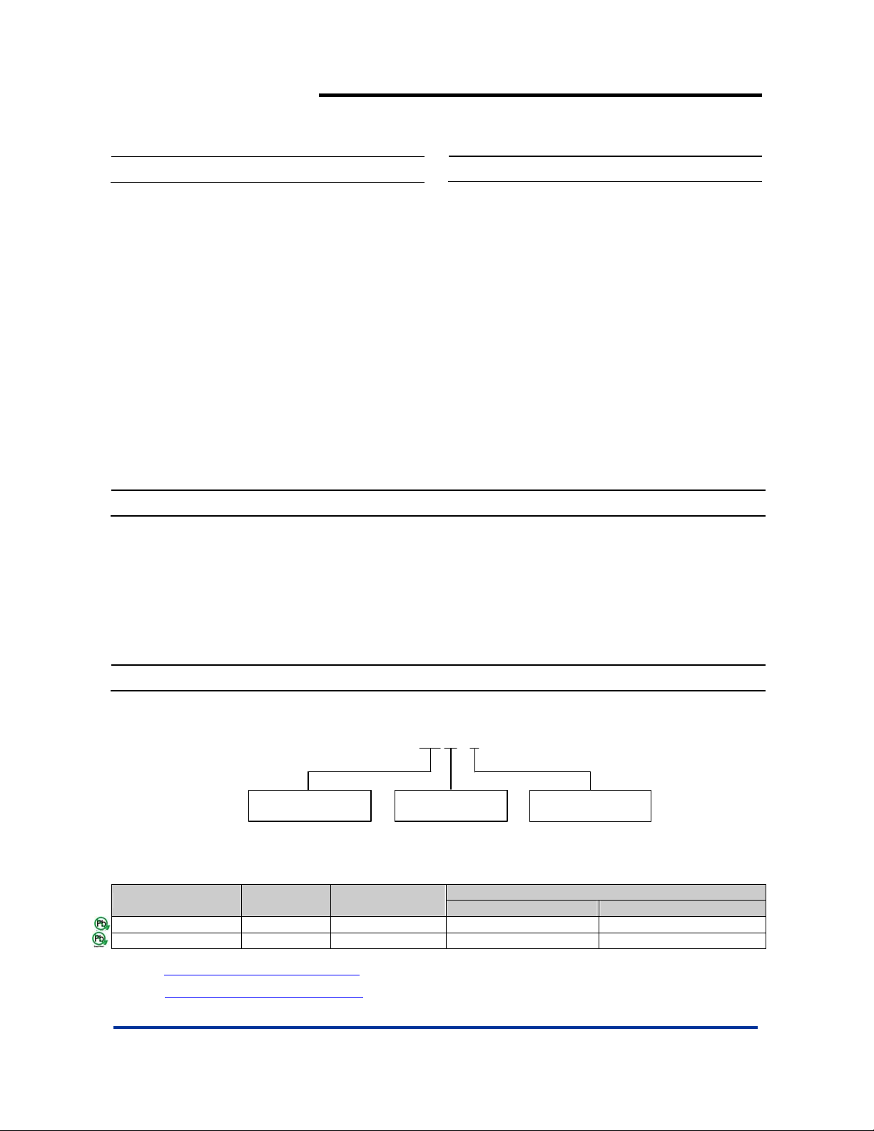
Pin Assignment
(Top View)
IN
1
AP133
300mA, LOW QUIESCENT CURRENT, FAST TRANSIENT
LOW DROPOUT LINEAR REGULATOR
(Top View)
5
OUT
EN
1
6
ADJ
2
GND
EN ADJ
SOT25
43
Pin Descriptions
Pin Name
IN 1 3
GND 2 2 Ground
EN 3 1 Enable input, active high
ADJ 4 6 Output feedback pin
NC 5 No connection
OUT 5 4
Pin Number
SOT25 DFN2020-6
Voltage input pin. Bypass to ground through at least 0.1µF
capacitor
Voltage output pin. Bypass to ground through 1µF ceramic
capacitor
2
GND
3
IN
DFN2020-6
Description
5
NC
OUT
4
AP133 Rev. 6 2 of 15 FEBRUARY 2009
www.diodes.com © Diodes Incorporated
Page 3
300mA, LOW QUIESCENT CURRENT, FAST TRANSIENT
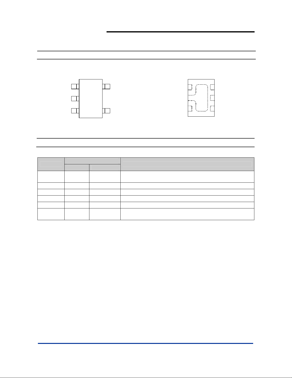
Functional Block Diagram
AP133
LOW DROPOUT LINEAR REGULATOR
IN
EN
Typical Application Circuit
V
IN
1uF
Enable
IN
EN
Gate
Driver
AP133
GND
Current Limit
and Thermal
Shutdown
0.8V
OUT
ADJ
R1
R2
OUT
FB
GND
V
OUT
1uF
⎛
⎜
1
VV
REFOUT
⎜
⎝
⎞
R
1
⎟
+=
⎟
R
2
⎠
AP133 Rev. 6 3 of 15 FEBRUARY 2009
www.diodes.com © Diodes Incorporated
Page 4
AP133
300mA, LOW QUIESCENT CURRENT, FAST TRANSIENT
LOW DROPOUT LINEAR REGULATOR
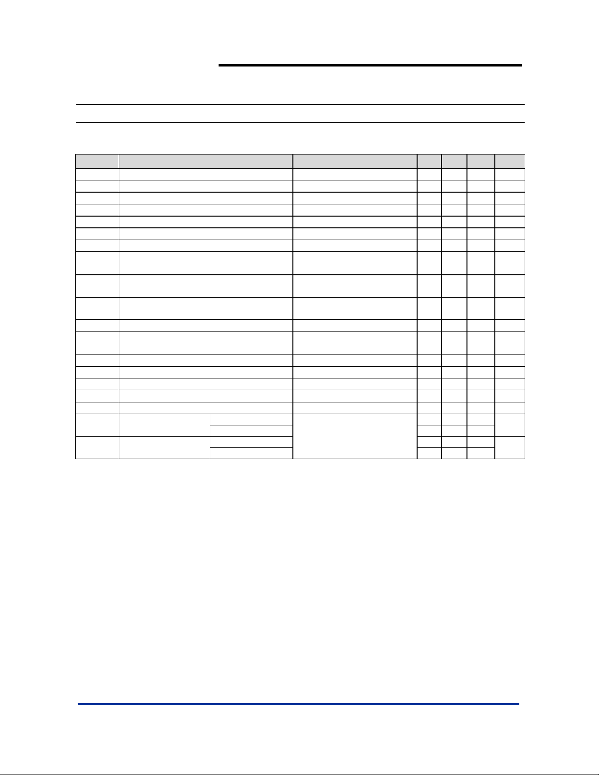
Absolute Maximum Ratings
Symbol Parameter Ratings Unit
VIN Input Voltage 7 V
OUT, ADJ, EN Voltage VIN + 0.3 V
Continuous Load Current Internal Limited
TOP Operating Junction Temperature Range -40 ~ 125 °C
TST Storage Temperature Range -65 ~150 °C
PD Power Dissipation (Note 3)
SOT25 740 mW
DFN2020-6 900 mW
TJ Maximum Junction Temperature 150 °C
Recommended Operating Conditions
Symbol Parameter Min Max Unit
V
I
OUT
T
Notes: 3. Ratings apply to ambient temperature at 25°C
AP133 Rev. 6 4 of 15 FEBRUARY 2009
Input voltage (No t e 4) 2 6 V
IN
Output Current 0 300 mA
Operating Ambient Temperature -40 85
A
4. At V
< 2.2V and TA< -20°C, the output current capability may be reduced.
IN
www.diodes.com © Diodes Incorporated
°C
Page 5
⎯
⎯
AP133
300mA, LOW QUIESCENT CURRENT, FAST TRANSIENT
LOW DROPOUT LINEAR REGULATOR
Electrical Characteristics
= 25oC, V
(T
A
Symbol Parameter Test Conditions Min Typ. Max Unit
I
Q
I
SHDN
I
LEAK
V
Dropout
V
REF
I
ADJ
V
OUT
ΔV
OUT
/ΔV
/V
IN
ΔV
OUT
/V
OUT
tST
PSRR
I
SHORT
I
LIMIT
V
IL
V
IH
I
EN
T
SHDN
T
HYS
θ
JA
θ
JC
AP133 Rev. 6 5 of 15 FEBRUARY 2009
= V
OUT
+1V, C
IN
Input Quiescent Current I
Input Shutdown Current VEN = 0V, I
Input Leakage Current VEN = 0V, OUT grounded
Dropout Voltage
ADJ reference voltage I
ADJ leakage
= 1uF, C
IN
OUT
= 1uF, V
= 2V, unless oth erwise stated)
EN
= 0~300mA
OUT
= 0
OUT
V
≥ 1.5V, I
OUT
= 0 0.8 V
OUT
= 300mA
OUT
40 60 uA
⎯
1 uA
⎯
1 uA
350 450 mV
1 uA
Output Voltage Accuracy -2 2 %
Line Regulation
Load Regulation I
Start-up Time
PSRR 1kHz, I
Short-circuit Current V
Current limit V
= V
V
IN
I
OUT
OUT
V
EN
I
OUT
= 5.0V, V
IN
OUT
+1V to 5.5V,
OUT
= 1mA
0.05 %/V
from 1mA to 300mA -1 1 %
= 0V to 2.0V,
= 300mA
= 0mA 65 dB
OUT
< 0.2V 120 mA
OUT
= 3V, R
= 3Ω 400 600 mA
OUT
25 us
EN Input Logic Low Voltage 0.4 V
EN Input Logic High Voltage 1.4 V
EN Input leakage V
= 0V or 5.5V -1 1 uA
EN
Thermal shutdown threshold 145
Thermal shutdown hysteresis 20
Thermal Resistance
Junction-to-Ambient
Thermal Resistance
Junction-to-Case
SOT25
DFN2020-6 142
SOT25 41
DFN2020-6 36
Device mounted on FR-4
substrate , 2oz copper, with
minimum recommended pad
layout.
176
www.diodes.com © Diodes Incorporated
°C
°C
o
C/W
o
C/W
Page 6

300mA, LOW QUIESCENT CURRENT, FAST TRANSIENT
Typical Performance Characteristics
AP133
LOW DROPOUT LINEAR REGULATOR
Output Voltag e vs . Temperature
3.3100
3.3050
3.3000
3.2950
Output Voltage (V)
3.2900
VIN=5V, Vout=3.3V
-50.0 -25.0 0.0 25.0 50.0 75.0 100.0 125.0
Temperature (°C)
Output Voltage vs. Input Voltage
2.0
1.8
1.6
1.4
1.2
1.0
0.8
0.6
Output Voltage (V)
0.4
0.2
0.0
0.01.02.03.04.05.06.0
Input Voltage (V)
IOUT=0mA
IOUT=150mA
1.8200
1.8150
1.8100
1.8050
Output Voltage (V)
1.8000
-50.0 -25.0 0.0 25.0 50.0 75.0 100.0 125.0
60
55
50
45
40
35
Quiescent Current (uA)
30
2.0 3.0 4.0 5.0 6.0
Output Voltage vs. Temperature
VIN=3.3V, Vout=1.8V
Temperature (°C)
Quiescent Current vs. Input Voltage
=1.2V
V
OUT
IOUT=0mA
IOUT=300mA
Input Voltag e (V)
Quiescent Current vs. I
V
=2.8V
OUT
60.00
55.00
50.00
45.00
40.00
35.00
Quiescent Current (uA)
30.00
0.00 50.00 100.00 150.00 200.00 250.00 300.00
Vin=3.3V
Vin=5V
I
OUT
OUT
(mA)
Quiescent Current vs. Temperature
50
45
40
35
Quiescent Current (uA)
30
-50.0 -25.0 0.0 25.0 50.0 75.0 100.0 125.0
VOUT=1.2V VIN=3.3V
VOUT=3.3V VIN=5.0V
Temperature (°C)
AP133 Rev. 6 6 of 15 FEBRUARY 2009
www.diodes.com © Diodes Incorporated
Page 7

300mA, LOW QUIESCENT CURRENT, FAST TRANSIENT
LOW DROPOUT LINEAR REGULATOR
Typical Performance Characteristics (Continued)
ADJ Pin Voltage vs. Input Voltage
V
OUT
0.8020
0.8015
0.8010
0.8005
0.8000
0.7995
ADJ Pin Voltage (V)
0.7990
2.0 3.0 4.0 5.0 6.0
Input Voltage (V)
450
400
350
300
250
200
150
100
50
Dropout Voltage (mV)
0
0.0 50.0 100.0 150.0 200.0 250.0 300.0
Dropout Voltage vs. I
=3.3V
I
(mA)
OUT
AP133
OUT
25°C
90°C
-45°C
Current Limit Protection
Time (50us/div)
Short Circuit Protection
Current Limit vs. Temperature
800
750
700
650
600
550
Current Limit (mA)
500
-50-30-101030507090
Vin=3.3V, Vout=1.2V
Vin=5.0V, Vout=3.3V
Temperature (°C)
Short Circuit Protection
Time (1ms/div)
Time (2ms/div)
AP133 Rev. 5 7 of 15 FEBRUARY 2009
www.diodes.com © Diodes Incorporated
Page 8

300mA, LOW QUIESCENT CURRENT, FAST TRANSIENT
LOW DROPOUT LINEAR REGULATOR
Typical Performance Characteristics (Continued)
AP133
Short Circuit Current vs. Input Voltage
150
140
130
120
110
100
90
80
70
Short Circuit Current (mA)
2.0 3.0 4.0 5.0 6.0
Input Voltage (V)
Thermal Shutdown Protection
Time (20ms/div)
Short Circuit Current vs. Temperature
150
140
130
120
110
100
90
Short Circuit Current (mA)
80
-50-30-101030507090
Vin=3.3V, Vout=1.2V
Vin=3.3V, Vout=1.8V
Vin=5.0V, Vout=3.3V
Temperature (°C)
PSRR
-20.00
-30.00
-40.00
-50.00
-60.00
PSRR (dB)
-70.00
-80.00
-90.00
100 1000 10000 100000
Freque ncy (Hz)
Line Transient Response
Time (20us/div)
Line Transient Response
Time (20us/div)
AP133 Rev. 5 8 of 15 FEBRUARY 2009
www.diodes.com © Diodes Incorporated
Page 9

300mA, LOW QUIESCENT CURRENT, FAST TRANSIENT
LOW DROPOUT LINEAR REGULATOR
Typical Performance Characteristics (Continued)
Line Transient Response
AP133
Line Transient Response
Time (20us/div)
Load Transient Response
Time (100us/div)
Load Transient Response
Time (20us/div)
Load Transient Response
Time (100us/div)
Load Transient Response
Time (20us/div)
AP133 Rev. 5 9 of 15 FEBRUARY 2009
www.diodes.com © Diodes Incorporated
Time (100us/div)
Page 10

300mA, LOW QUIESCENT CURRENT, FAST TRANSIENT
LOW DROPOUT LINEAR REGULATOR
Typical Performance Characteristics (Continued)
Start-up Time
AP133
Start-up Time
Time (5us/div)
Start-up Time
Time (5us/div)
Time (5us/div)
Start-up Time
Time (5us/div)
AP133 Rev. 5 10 of 15 FEBRUARY 2009
www.diodes.com © Diodes Incorporated
Page 11

AP133
300mA, LOW QUIESCENT CURRENT, FAST TRANSIENT
LOW DROPOUT LINEAR REGULATOR
Application Note
Input Capacitor
A1μF ceramic capacitor is recommended to connect between
and GND pins to decouple input power supply glitch and
V
IN
noise. The amount of the capacitance may be increased
without limit. This i nput capacitor must be located as close as
possible to the device to assure input stability and less noise.
For PCB layout, a wide copper trace is required for both V
GND. A lower ESR capacitor allows the use of less
capacitance, while higher ESR type require more capacitance.
IN
and
Output Capacitor
The output capacitor is required to stabilize and help transient
response for LDO. The AP133 is stable with very small ceramic
output capacitors. The recommended capacitance is from 1μF
to 4.7μF, Equivalent Series Resistance (ESR) is from 10mΩ to
100mΩ, and temperature characteristics is X7R or X 5R . H igh er
capacitance values help to improve load/line transient
response. The output capacitance may be increased to keep
low undershoot/overshoot. Place output capacitor as close as
possible to OUT and GND pins, and keep the leads as short as
possible.
Adjustable Opera ti on
The AP133 provides output voltage from 1.0V to 5.0V through
external resistor divider as shown below.
EN
AP133
IN
RR
OUT
ADJ
GN
D
⎛
⎜
VV
REFOUT
⎜
⎝
⎛
V
OUT
⎜
21
⎜
V
REF
⎝
⎞
R
1
⎟
1
+=
⎟
R
2
⎠
⎞
⎟
−= 1
⎟
⎠
V
OUT
C
OUT
R1
R2
2
V
IN
C
IN
Enable
The output voltage is calculated by:
Where V
Rearranging the equation will give the following that is used for
adjusting the output to a particular voltage:
To maintain the s tability of the internal ref erence voltage, R
needs to be kept smaller than 250kΩ.
=0.8V (the internal reference voltage)
REF
No Load Stability
Other than external resistor divider, no minimum load is
required to keep the device stable. The device will remain
stable and regulated in no load condition.
AP133 Rev. 6 11 of 15 FEBRUARY 2009
www.diodes.com © Diodes Incorporated
ON/OFF Input Operation
The AP133 is turned on by setting the EN pin high, and is
turned off by pulling it low. If this feature is not used, the EN pin
should be tied to IN pin to keep the regulator output on at all
time. To ensure proper operation, the signal source used to
drive the EN pin must be able to swing above and below the
specified turn-on/off voltage thresholds listed in the Electrical
Characteristics section under V
and VIH.
IL
Current Limit Protection
When output current at OUT pin is higher than current limit
threshold, the current limit protection will be triggered and
clamp the output current to approximately 600mA to prevent
over-current and to protect the regulator from damage due to
overheating.
Short Circuit Protection
When OUT pin is short-circuit to GND or OUT pin voltage is
less than 200mV, short circuit protection will be triggered and
clamp the output current to approximately 120mA. This feature
protects the regulator from over-current and damage due to
overheating.
Thermal Shutdown Protection
Thermal protection disables the output when the junction
temperature rises to approximately +145°C, allowing the device
to cool down. When the junction temperature reduces to
approximately +125°C the output circuitry is enabled again.
Depending on power dissipation, thermal resistance, and
ambient temperature, the thermal protection circuit may cycle
on and off. This cycling limits the heat dissipation of the
regulator, protecting it from damage due to overheating.
Ultra Fast Start-up
After enabled, the AP133 is able to provide full power in as little
as tens of microseconds, typically 25µs, without sacrificing low
ground current. This f ea ture will help load circ uit ry m o ve in a n d
out of standby mode in real time, eventually extend battery life
for mobile phones and other portable devices.
Fast Transient Response
Fast transient response LDOs can also extend battery life.
TDMA-based cell phone protocols such as Global System for
Mobile Communications (GSM) have a transmit/receive duty
factor of only 12.5 percent, enabling power savings by putting
much of the baseba nd circuitr y into standby mod e in between
transmit cycles. In baseband circuits, the load often transitions
virtually instantaneously from 100µA to 100mA. To meet this
load requirement, the LDO must react very quickly without a
large voltage drop or overshoot — a requirement that cannot
be met with conventional, general-purpose LDOs.
The AP133’s fast transient response from 0 to 300mA provides
stable voltage supply for fast DSP and GSM chipset with fast
changing load.
Small Overshoot and Undershoot
The AP133 has small and controlled overshoot and undershoot
in load and line transitions. This helps to protect supplied circuit
from damage and operation error caused by glitches. This
feature also permits the usage of small value ou tput decoup ling
capacitor with AP133.
Page 12

300mA, LOW QUIESCENT CURRENT, FAST TRANSIENT
Application Note
Low Quiescent Current
Cellular phone baseband internal digital circuits typically
operate from 1.8V to 2.6V. When the Li+ battery voltage falls to
3.2-3.3V, most phones shut off, giving at least 500-600mV of
headroom for the baseband digital LDO, so dropout is not
critical. Output noise and the PSRR are not critical specs for
the digital circuits. Nonetheless, this supply requires low
quiescent curren t at light loads becau se this LDO stays on at
all times. Figure below shows how the digital supply current of
a representative GSM chipset core varies as a function of time.
In the standby mode, the microprocessor consumes only
around 200µA. Since the phone stays in standby for the
longest percentage of time, using a 40µA quiescent current
LDO, instead of 140µA, saves 100µA and extends the standby
time by 340µA/240µA, or 1.417 times.
AP133
LOW DROPOUT LINEAR REGULATOR
The baseband internal analog circuit is typically 2.4V-3.0V, and
it requires 200-600mV dropout. This LDO is on all the time, so it
requires low quiescent current as well. The cellular phone
real-time clock LDO needs a very low quiescent current, since
this LDO is on all the time even though the handset is powered
off.
The AP133, consuming only around 40µA for all input range
and output loading, provides great power saving in portable
and low power applications.
Wide Output Range
The AP133, with a wide output range of 1.0V to 5.0V, provides
a versatile LDO solution for many portable applications.
High PSRR
The RF circuit consists of receive and transmit sections, which
typically require 2.6V-3.0V supply volta ge. The R F circuits su ch
as LNA (low-noise amplifier), up/down-converter, mixer, PLL,
VCO, and IF stage, require low noise and high PSRR LDOs.
The temperature-compensated crystal oscillator circuit requires
very high PSRR at RF power amplifier burst frequency. For
instance, minimum 65dB PSRR at 217Hz is recommended for
the GSM handsets.
In order to provide good audio quality, the audio power supply
for hand-free, game, MP3, and multimedia applications in
cellular phones, require low-noise and high PSRR at audio
frequency range (20Hz-20kHz).
The AP133, with PSRR of 70dB at 1kHz in best case, is
suitable for some of these applications that require high PSRR.
AP133 Rev. 6 12 of 15 FEBRUARY 2009
www.diodes.com © Diodes Incorporated
Page 13

Marking Information
(1) SOT25
AP133
300mA, LOW QUIESCENT CURRENT, FAST TRANSIENT
LOW DROPOUT LINEAR REGULATOR
( Top View )
W X
7
4
XX : Identification code
Y
: Year 0~9
: Week : A~Z : 1~26 week;
W
a~z : 27~52 week; z represents
52 and 53 week
X
: A~Z : Green
(2) DFN2020-6
5
XX
Y
1 2 3
Part Number Package Identification Code
AP133-W SOT25 NB
( Top View )
XX
: Identification Code
X X
Y
W
X
Y : Year : 0~9
: Week : A~Z : 1~26 week;
W
a~z : 27~52 week; z represents
52 and 53 week
X
: A~Z : Green
Part Number Package Identification Code
AP133-SN DFN2020-6 NB
AP133 Rev. 6 13 of 15 FEBRUARY 2009
www.diodes.com © Diodes Incorporated
Page 14

300mA, LOW QUIESCENT CURRENT, FAST TRANSIENT
Package Information (All Dimensions in mm)
(1) Package Type: SOT25
AP133
LOW DROPOUT LINEAR REGULATOR
(2) Package Type: DFN2020-6
0.57/0.63
0.05 C
0.08 C
B
1.95/2.075
0.15 C
2x-
0/0.05
2x
0.76/0.96
1
.
0
R
0.65nom.
C
0.15
Bottom View
1.95/2.075
1.45/1.65
Marking
0.15max.
A
0.30/0.40
0.2/0.3
Pin#1 ID
0.43mon.
(Active area depth)
Seating plane
C
0.05
M C A B
AP133 Rev. 6 14 of 15 FEBRUARY 2009
www.diodes.com © Diodes Incorporated
Page 15

Taping Orientation
AP133
300mA, LOW QUIESCENT CURRENT, FAST TRANSIENT
LOW DROPOUT LINEAR REGULATOR
Notes: 5. The taping orientation of the other package type can be found on our website at http://www.diodes.com/datasheets/ap02007.pdf
IMPORTANT NOTICE
Diodes Incorporated and its subsidiaries reserve the right to make modifications, enhancements, improvements, corrections or other changes without further
notice to any product herein. Diodes Incorporated does not assume any liability arising out of the application or use of any product described herein; neither
does it convey any license under its patent rights, nor the rights of others. The user of products in such applications shall assume all risks of such use and will
agree to hold Diodes Incorporated and all the companies whose products are represented on our website, harmless against all damages.
LIFE SUPPORT
Diodes Incorporated products are not authorized for use as critical components in life support devices or systems without the expressed written approval of the
President of Diodes Incorporated.
AP133 Rev. 6 15 of 15 FEBRUARY 2009
www.diodes.com © Diodes Incorporated
 Loading...