Page 1

AP1184
4A ULTRA LOW DROPOUT POSITIVE ADJUSTABLE OR
FIXED-MODE REGULATOR
Features
General Description
• 0.85V maximum dropout voltage at 4A load current
• Built-in Thermal shutdown
• Output current limiting
• Adjustable or fixed output voltage1.5V, 1.8V, 2.5V,
3.3V, 5.0V
• Fast transient response
• Good noise rejection
• Packages: TO220-5L and TO263-5L
• Lead Free Finish/ RoHS Complian (Note 1)
AP1184 is a 4A regulator with extremely low dropout voltage.
This product is specifically designed to provide well regulated
supply for applications requiring 2.8V or lower voltages from 3.3V
ATX power supplies where high efficiency of the switch can be
achieved without the cost and complexity associated with
switching regulator. One such application is the new graphic
chipsets that requires anywhere from 2.4V to 2.7V supply.
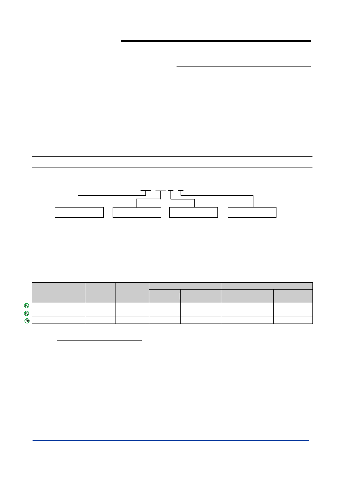
Ordering Information
XX
Vout
Package
K5 : TO263-5L
T5 : TO220-5L
AP1184
Blank : Adj
15 = 1.5V
18 = 1.8V
25 = 2.5V
33 = 3.3V
50 = 5.0V
Device
AP1184K5XXL-U K5 TO263-5L 50 -U NA NA
Lead-free
AP1184K5XXL-13 K5 TO263-5L NA NA 800/Tape & Reel -13
Lead-free
AP1184T5XXL-U T5 TO220-5L 50 -U NA NA
Lead-free
Notes: 1. EU Directive 2002/95/EC (RoHS). All applicable RoHS exemptions applied, see EU Directive 2002/95/EC Annex Notes.
2. Pad layout as shown on Diodes Inc. suggested pad layout document AP02001, which can be found on our website at
http://www.diodes.com/datasheets/ap02001.pdf
Package
Code
Packaging
(Note 2)
.
L X
XX
-
Quantity
-
Lead Free
L : Lead Free
Tube 13” Tape and Reel
Part Number
Suffix
Packing
U : Tube
13 : Tape & Reel
Quantity
Part Number
Suffix
AP1184 Rev. 5 1 of 12 SEPTEMBER 2008
www.diodes.com © Diodes Incorporated
Page 2

A
Pin Assignments
FRONT VIEW
5
4
3
2
1
Tab is Vout
AP1184
4A ULTRA LOW DROPOUT POSITIVE ADJUSTABLE OR
FIXED-MODE REGULATOR
Vin
Vctrl
Vout
Adj(GND)
Vsense
FRONT VIEW
5
4
3
2
1
Tab is Vout
Vin
Vctrl
Vout
Adj(GND)
Vsense
TO263-5L
Pin Descriptions
Pin Numbers with standard type are for TO220-5L, TO263-5L packages.
Name I/O Description
Adj
(GND)
resistor divider from this pin to the Vout pin and ground sets the output voltage. (GND
only for fixed mode)
This pin is the positive side of the reference that allows remote load sensing to achieve
Vsense I
excellent load regulation. A minimum of 10uF capacitor must be connected from this pin
to ground to insure stability.
The input of the regulator. Typically a large storage capacitor is connected from this pin
Vin I
to ground to insure that the input voltage does not sag below the minimum dropout
voltage during the load transient response. This pin must always be higher than Vout in
order for the device to regulate.
This pin is the supply pin for the internal control circuit as well as the base drive for the
Vctrl I
pass transistor. This pin must always be higher than the Vout pi n in ord er to regu late the
device. A minimum of 100uF capacitor must be connected from this pin to ground to
insure stability.
Vout O
The output of the regulator. A minimum of 100uF capacitor must be connected from this
pin to ground to insure stability.
Block Diagram
TO220-5L
Vin
Vctrl
CURRENT
LIMIT
THERMAL
SHUTDOWN
+
+
-
1.25V
+
+
-
Vout
Vsense
Adj
AP1184 Rev. 5 2 of 12 SEPTEMBER 2008
www.diodes.com © Diodes Incorporated
Page 3

AP1184
4A ULTRA LOW DROPOUT POSITIVE ADJUSTABLE OR
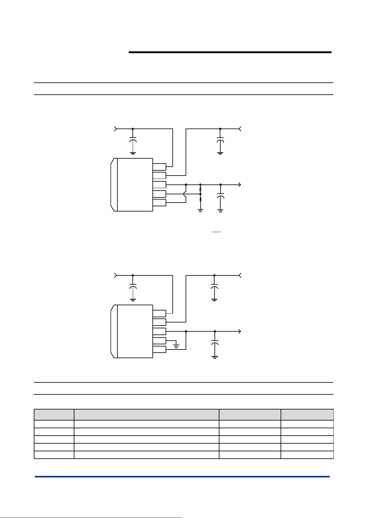
Typical Application Circuit
(1) Adjustable Regulator
3.3V
FIXED-MODE REGULATOR
5V
470µF
Vctrl
Vout
Vsense
Tab is Vout
(2) 3.3V to 2.5V Fixed Mode Regulator
3.3V
470µF
Vctrl
Vout
GND
Vsense
Vin
Adj
Vin
V:Note +×=
OUT
V
REF
R1
R2
121
121
1(
470µF
Ω
Ω
2.5V/ 4A
470µF
R
2
)
R
1
5V
470µF
2.5V/ 4A
470µF
Tab is Vout
Absolute Maximum Ratings
Symbol Parameter Rating Unit
VIN Input Voltage 16 V
V
Control Input voltage 18 V
ctrl
PD Power dissipation Internally limited
TST Storage temperature Range -65 to +150
TOP Operation Junction Temperature Range 0 to +125
AP1184 Rev. 5 3 of 12 SEPTEMBER 2008
www.diodes.com © Diodes Incorporated
o
C
o
C
Page 4

AP1184
4A ULTRA LOW DROPOUT POSITIVE ADJUSTABLE OR
FIXED-MODE REGULATOR
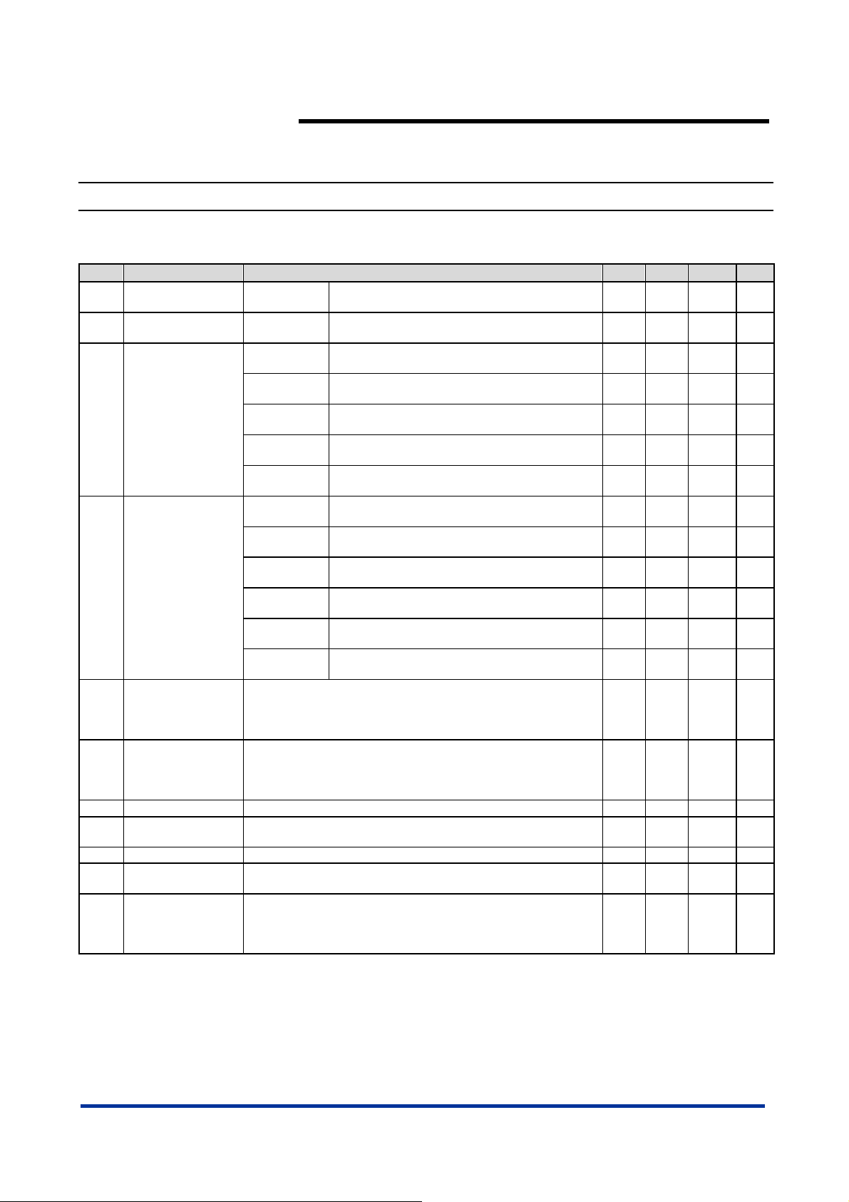
Electrical Characteristics (Under Operating Conditions)
Unless otherwise specified, these specifications apply over, Cin = 1uF, C
V
out
= V
sense
Sym. Parameter Test Condition Min Typ. Max Unit
=10mA, TA = 25oC, (Vin-V
I
V
Reference Voltage AP1184-Adj
REF
Line Regulation AP1184-XXX
AP1184-1.5
AP1184-1.8
V
Output Voltage
out
AP1184-2.5
AP1184-3.3
AP1184-5.0
AP1184-Adj
AP1184-1.5
Load
Regulation
AP1184-1.8
AP1184-2.5
AP1184-3.3
AP1184-5.0
= 0V for all conditions below.
V
adj
Dropout Voltage
–V
(V
)
ctrl
out
Dropout Voltage
(Vin – V
out
)
Current Limit
Minimum Load
Current
= 2.05V, Io = 1.5A
V
in
V
= 2.05V, Io = 3A
in
= 2.05V, Io = 4A
V
in
V
= 0V for all conditions below.
adj
V
= 2.75V, Io = 1.5A
ctrl
= 2.75V, Io = 3A
V
ctrl
V
=2.75V, Io =4A
ctrl
V
= 2.75V, Vin = 2.05V, ΔVo = 100mV, V
ctrl
V
= 5V, Vin = 3.3V, V
ctrl
Thermal Regulation 30mS Pulse 0.01 0.02 %/W
Ripple Rejection
Vctrl = 5V, Vin = 5V, Io = 4A, Vadj = 0V, Tj = 25, Vripple =1Vpp
at 120Hz
Vadj = 0V for all conditions below.
Control Pin Current
Vctrl = 2.75V, Vin = 2.05V, Io = 1.5A
Vctrl = 2.75V, Vin = 2.05V, Io = 3A
Vctrl = 2.75V, Vin = 2.05V, Io = 4A
o
= VIN+1V
V
ctrl
= 10mA, V
I
O
V
= VIN+1V
ctrl
= 10mA, TA = 25oC, 2.2VVIN12V
I
OUT
= VIN+1V
V
ctrl
= 10mA, TA = 25oC, 2.5VVIN12V
I
OUT
V
= VIN+1V
ctrl
= 10mA, TA = 25oC, 3.2VVIN12V
I
OUT
= VIN+1V
V
ctrl
= 10mA, TA = 25oC, 4.0VVIN12V
I
OUT
V
= VIN+1V
ctrl
= 10mA, TA = 25oC, 5.7VVIN12V
I
OUT
= VIN+1V
V
ctrl
0mA<Io<4A, T
(V
- V
IN
= 3V, 0mA<Io<4A, TA = 25oC
V
IN
= 4V
V
ctrl
= 3.3V, 0mA<Io<4A, TA = 25oC
V
IN
V
= 4.3V
ctrl
= 4V, 0mA<Io<4A, TA = 25oC
V
IN
= 5V
V
ctrl
= 5V, 0mA<Io<4A, TA = 25oC
V
IN
V
= 6V
ctrl
= 8V, 0mA<Io<4A, TA = 25oC
V
IN
V
= 9V
ctrl
OUT
A
) =2V ,V
OUT
= 0V 5 10 mA
adj
= 10uF, and Tj = 0 to 150oC. Typical value refer to TA = 25oC.
out
) = 0.7V,
out
+0.7V<VIN<12V, TA = 25oC
1.225 1.250 1.275 V
0.2 %
1.470 1.500 1.530 V
1.764 1.800 1.836 V
2.450 2.500 2.550 V
3.235 3.300 3.365 V
4.900 5.000 5.100 V
= 25oC
= VIN + 1V
ctrl
1 %
12 15 mV
15 18 mV
20 25 mV
26 33 mV
40 50 mV
1.10
0.26
0.50
0.70
adj
= 0V
4.2 A
60 70 dB
6
30
33
1.15
1.18
1.25
0.38
0.60
0.85
25
60
70
V
mA
V
AP1184 Rev. 5 4 of 12 SEPTEMBER 2008
www.diodes.com © Diodes Incorporated
Page 5

AP1184
4A ULTRA LOW DROPOUT POSITIVE ADJUSTABLE OR
FIXED-MODE REGULATOR
Electrical Characteristics (Continued)
Unless otherwise specified, these specifications apply over, Cin = 1uF, C
V
= V
t
ou
sense
.
Sym. Parameter Test Condition Min Typ. Max Unit
I
adj
Adjust Pin Current
= 2.75V, Vin = 2.05,V
V
ctrl
adjj
= 0
= 10uF, and Tj = 0 to 150oC. Typical value refer to TA = 25oC.
out
50 150 µA
θ
Thermal Resistance
JA
Junction-to-Ambient
θ
Thermal Resistance
JC
Junction-to-Case
Notes: 3. AP1184-ADJ incorporates an internal thermal shutdown that protects the device when the junction temperature exceeds the allowable
maximum junction temperature.
4. Test conditions for TO263-5L : Devise mounted on 2oz copper, minimum recommended pad layout , FR-4 PCB.
5. Test conditions for TO220-5L : with copper area of approximately 3in
TO263-5L: Control Circuitry/Power Transistor (Note 4)
TO220-5L: Control Circuitry/Power Transistor (Note 5)
TO263-5L: Control Circuitry/Power Transistor (Note 4)
TO220-5L: Control Circuitry/Power Transistor (Note 5)
2
, 1oz.
61
31
7
5
O
C/W
O
C/W
O
C/W
O
C/W
Package Max Pd. Remarks
TO263-5L/TO220-5L 2.4W~4.4W With heat sink or amount of copper board needed.
Functional Descriptions
Introduction
The AP1184 regulator is a 5 terminal device designed specifically to provide extremely low dropout voltages comparable to the PNP type
without the disadvantage of the extra power dissipation due to the base current associated with PNP regulators. This is done by bringing
out the control pin of the regulator that provides the base current to the power NPN and connecting it to a voltage that is greater than the
voltage present at the
motherboard with an ATX style power supply that provides 5V and 3.3V to the board. One such application is the new graphic chip sets
that require anywhere from 2.4V to 2.7V supply. The AP1184 can easily be programmed with the addition of two external resistors to any
voltages within the range of 1.25V to 15.5V. Another major requirement of these graphic chips is the need to switch the load current from
zero to several amps in tens of nanoseconds at the processor pins, which translates to an approximately 300 to 500ns of current step at
the regulator. In addition, the output voltage tolerances are also extremely tight and they include the transient response as part of the
specification.
The AP1184 is specifically designed to meet the fast current transient needs as well as providing an accurate initial voltage, reducing the
overall system cost with the need for fewer number of output capacitors. Another feature of the device is its true remote sensing capability
that allows accurate voltage setting at the load rather than at the device.
Output Voltage Setting
The AP1184-ADJ can be programmed to any voltages in the range of 1.25V to 15.5V with the addition of R1 and R2 external resistors
according to the following formula:
V
pin. This flexibility makes the AP1184 ideal for applications where dual inputs are available such as a computer
in
AP1184 Rev. 5 5 of 12 SEPTEMBER 2008
www.diodes.com © Diodes Incorporated
Page 6

AP1184
4A ULTRA LOW DROPOUT POSITIVE ADJUSTABLE OR
Functional Descriptions (Continued)
Vout = Vref (1+R2/R1) + Iadj * R2 where : Vref = 1.25V & Iadj=50uA Typically
FIXED-MODE REGULATOR
Vin
Vctrl
AP1184-ADJ
Adj
Iadj=50uA
Vsense
Vref
R1+
R2+
Vout
The AP1184-ADJ keeps a constant 1.25V between the Vsense pin and the Adj pin. By placing a resistor R1 across these two pins and
connecting the Vsense and Vout pin together, a constant current flows through R1, adding to the Iadj current and into the R2 resistor
producing a voltage equal to the (1.25/R1)*R2 + Iadj*R2. This voltage is then added to the 1.2 5V to set the output voltage. This is
summarized in the above equation. Since the minimum load current requirement of the AP1184-ADJ is 10mA, R1 is ty pically selected to
be a 121Ω resistor so that it automatically satisfies this condition. Notice that since the Iadj is typically in the range of 50uA it only adds a
small error to the output voltage and should be considered when very precise output voltage setting is required.
Load Regulation
Since the AP1184 has separate pins for the output (Vout) and the sense (Vsense), it is ideal for providing true remote sensing of the
output voltage at the load. This means that the voltage drops due to parasitic resistance such as PCB traces between the regulator and
the load are compensated for using remote sensing. Figure following shows a typical application of the AP1184-ADJ with remote sensing.
Vin
Vctrl
Vin
Vctrl
AP1184-ADJ
Adj
Vout
Vsense
R1
R
L
R2
Stability
The AP1184-XXX requires the use of an output capacitor as part of the frequency compensation in order to make the regulator stable.
Typical designs for the microprocessor applications use standard electrolytic capacitors with typical ESR in the range of 50 to 100mΩ
and an output capacitance of 100uF to 1000uF. Fortunately as the capacitance increases, the ESR dec reases resulting in a fixed RC
time constant. The AP1184-XXX takes advantage of the phenomena in making the overall regulator loop stable. For most applications a
minimum of 100uF aluminum electrolytic capacitor insures both stability and good transient response.
Thermal Design
The AP1184-XXX incorporates an internal thermal shutdown that protects the device when the junction temperature exceeds the
allowable maximum junction temperature. Although this device can operate with junction temperatures in the range of 150
recommended that the selected heat sink be chosen such that during maximum continuous load operation, the junction temperature is
kept below this number. The example below shows the steps in selecting the proper surface mount package.
o
C, it is
AP1184 Rev. 5 6 of 12 SEPTEMBER 2008
www.diodes.com © Diodes Incorporated
Page 7

AP1184
4A ULTRA LOW DROPOUT POSITIVE ADJUSTABLE OR
FIXED-MODE REGULATOR
Functional Descriptions (Continued)
Assuming, the following conditions:
= 2.5V
V
out
V
= 3.3V
in
V
= 5V
ctrl
I
= 2A DC Avg.
out
Calculate the maximum power dissipation using the following equation:
= I
P
P
Using table below select the proper package and the amount of copper board needed.
* ( Vin - V
d
out
= 2 * (3.3-2.5) + (2/60) * (5-2.5) = 1.68W
d
Package Copper Area θ
TO263-5L Pad Size-1.4”X1.4” 25-45 2.4W-4.4W 2.0W-3.6W
Notes: 6. Above table is based on the maximum junction temperature of 135oC.
As shown in the above table, any of the two packages will do the job.
out
) + ( I
/60) * ( V
out
ctrl
- V
)
out
(oC/W) Max Pd (TA = 25oC) Max Pd (TA = 45oC)
JA
AP1184 Rev. 5 7 of 12 SEPTEMBER 2008
www.diodes.com © Diodes Incorporated
Page 8

4A ULTRA LOW DROPOUT POSITIVE ADJUSTABLE OR
Performance Characteristics
1200
Vpower = 2.05 V
1100
1000
Tj = 20 oC
900
Tj = 120 oC
Vcontrol Dropout Voltage (mV)
800
0
V
control
0.5
1.5
1.0
Output Current (A)
2.0
2.5 3.0 3.5 4.0
Dropout Voltage vs Output Current
FIXED-MODE REGULATOR
800
Vcontrol = 2.75 V
750
700
650
600
550
500
450
400
350
300
250
200
150
Vpower Dropout Voltage (mV)
100
50
0
0
V
power
0.5
Dropout Voltage vs Output Current
Tj = 120 oC
1.0
1.5 2.0
Output Current (A)
AP1184
Tj = 20 oC
2.5
3.0 3.5 4.0
1. 253
1. 252
1. 251
1. 250
1. 249
Reference Voltage (V)
1. 248
1. 247
20
0
40 60 80 100 120
Junction Temperature (oC)
Reference Voltage vs Junction Temperature
0. 15
0. 14
0. 12
0. 10
0. 08
0. 06
0. 04
Load Regulation (%)
0. 02
0
0.5 1.0 1.5 2.0 2.5 3.0 3.5 4.0
0
Load Regulation vs Output Current
Tj = 120 oC
Tj = 20 oC
Output Current (A)
AP1184 Rev. 5 8 of 12 SEPTEMBER 2008
www.diodes.com © Diodes Incorporated
Page 9

4A ULTRA LOW DROPOUT POSITIVE ADJUSTABLE OR
Performance Characteristic (Continued)
AP1184
FIXED-MODE REGULATOR
Transient Response
V
CONTROL
= 3.3V
V
POWER
= 2.5V
V
OUT
C
CONTROL
= 100uF
C
POWER
C
= 0.1uF
ADJ
= 470uF
C
OUT
I
LOAD
10mA to 4A
= 5.0V
=10uF
AP1184 Rev. 5 9 of 12 SEPTEMBER 2008
www.diodes.com © Diodes Incorporated
Page 10

Marking Information
(1) TO263-5L
1184-XX: Voltage
1184: Adj
1184-15 : 1.5V
1184-18 : 1.8V
1184-25 : 2.5V
1184-33 : 3.3V
1184-50 : 5.0V
AP1184
4A ULTRA LOW DROPOUT POSITIVE ADJUSTABLE OR
FIXED-MODE REGULATOR
( Top View )
Logo
1184-XX
YY WW
X
X
L : Lead Free
ID code
Xth week : 01~52
Year :
"07" = 2007
"08" = 2008
~
(2) TO220-5L
1184-XX: Voltage
1184: Adj
1184-15: 1.5V
1184-18: 1.8V
1184-25: 2.5V
1184-33: 3.3V
1184-50: 5.0V
( Top view )
1184-XX
YY WW X X
Logo
L : Lead Free Package
ID code
Xth week: 01~52
Year:
"07" = 2007
"08" = 2008
~
AP1184 Rev. 5 10 of 12 SEPTEMBER 2008
www.diodes.com © Diodes Incorporated
Page 11

4A ULTRA LOW DROPOUT POSITIVE ADJUSTABLE OR
Package Information (All Dimensions in mm)
(1) Package Type: TO263-5L
AP1184
FIXED-MODE REGULATOR
(2) Package Type: TO220-5L
AP1184 Rev. 5 11 of 12 SEPTEMBER 2008
www.diodes.com © Diodes Incorporated
Page 12

AP1184
4A ULTRA LOW DROPOUT POSITIVE ADJUSTABLE OR
FIXED-MODE REGULATOR
IMPORTANT NOTICE
Diodes Incorporated and its subsidiaries reserve the right to make modifications, enhancements, improvements, corrections or other changes without further
notice to any product herein. Diodes Incorporated does not assume any liability arising out of the application or use of any product described herein; neither
does it convey any license under its patent rights, nor the rights of others. The user of products in such applications shall assume all risks of such use and will
agree to hold Diodes Incorporated and all the companies whose products are represented on our website, harmless against all damages.
LIFE SUPPORT
Diodes Incorporated products are not authorized for use as critical components in life support devices or systems without the expressed written approval of the
President of Diodes Incorporated.
AP1184 Rev. 5 12 of 12 SEPTEMBER 2008
www.diodes.com © Diodes Incorporated
 Loading...