Diodes AP1117, AP1117I User Manual

AP1117/AP1117I
1A DROPOUT POSITIVE ADJUSTABLE OR FIXED-MODE REGULATOR
Description
AP1117 is a low dropout positive adjustable or fixed-mode regulator
with 1A output current capability. The product is voltage specifically
designed to provide well-regulated supply for low IC applications such
as high-speed bus termination and low current 3.3V logic supply.
AP1117 is also well suited for other applications such as VGA cards.
AP1117 is guaranteed to have lower than 1.4V dropout at full load
current making it ideal to provide well-regulated outputs of 1.25 to 5.0
with 6.4V to 18V input supply. AP1117 is available both in commercial
temperature grade (AP1117) and in industrial temperature range
(AP1117I) (TO252 and SOT223).
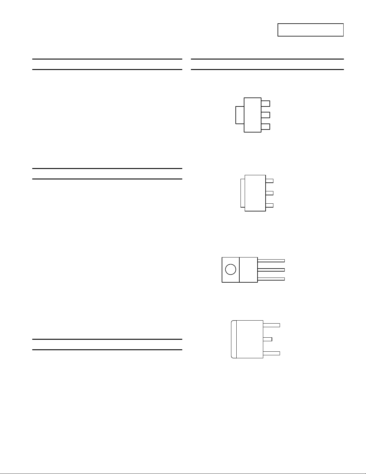
Pin Assignments
SOT89-3
( Top View )
3
2
1
Tab is V
( Top View )
OUT
SOT223
VIN
OUT
V
Adj (GND)
Features
3
VIN
1.4V Maximum Dropout at Full Load Current
Fast Transient Response
Output Current Limiting
Built-in Thermal Shutdown
Good Noise Rejection
3-Terminal Adjustable or Fixed 1.5V, 1.8V,2.5V, 3.3V, 5.0V
Operating Junction Temperature range
0°C T
-20°C T
-40°C T
Lead-Free Packages: SOT223, TO252, SOT89-3, TO263 and
TO220-3
Totally Lead-Free; RoHS Compliant (Notes 1 & 2)
SOT223, TO252, SOT89-3, TO263 and TO220-3: Available in
“Green” Molding Compound (No Br, Sb)
Halogen and Antimony Free. “Green” Device (Note 3)
+125°C (All packages)
J
+125°C (see ordering information)
J
+125°C (see ordering information)
J
( Front View )
( Top View )
2
1
Tab is V
Tab is VOUT
OUT
TO220-3
3
2
1
TO252 and TO263
3
2
VOUT
VOUT
Adj (GND)
V
IN
V
OUT
Adj (GND)
IN
V
Applications
PC Peripheral
Communication
Consumer Equipment
Notes: 1. No purposely added lead. Fully EU Directive 2002/95/EC (RoHS) & 2011/65/EU (RoHS 2) compliant.
2. See http://www.diodes.com quality/lead_free.html for more information about Diodes Incorporated’s definitions of Halogen and Antimony free, "Green"
and Lead-Free.
3. Halogen and Antimony free "Green” products are defined as those which contain <900ppm bromine, <900ppm chlorine (<1500ppm total Br + Cl) and
<1000ppm antimony compounds.
1
Tab is VOUT
Adj (GND)
AP1117/AP1117I
Document number: DS31009 Rev. 23 - 2
1 of 13
www.diodes.com
June 2013
© Diodes Incorporated

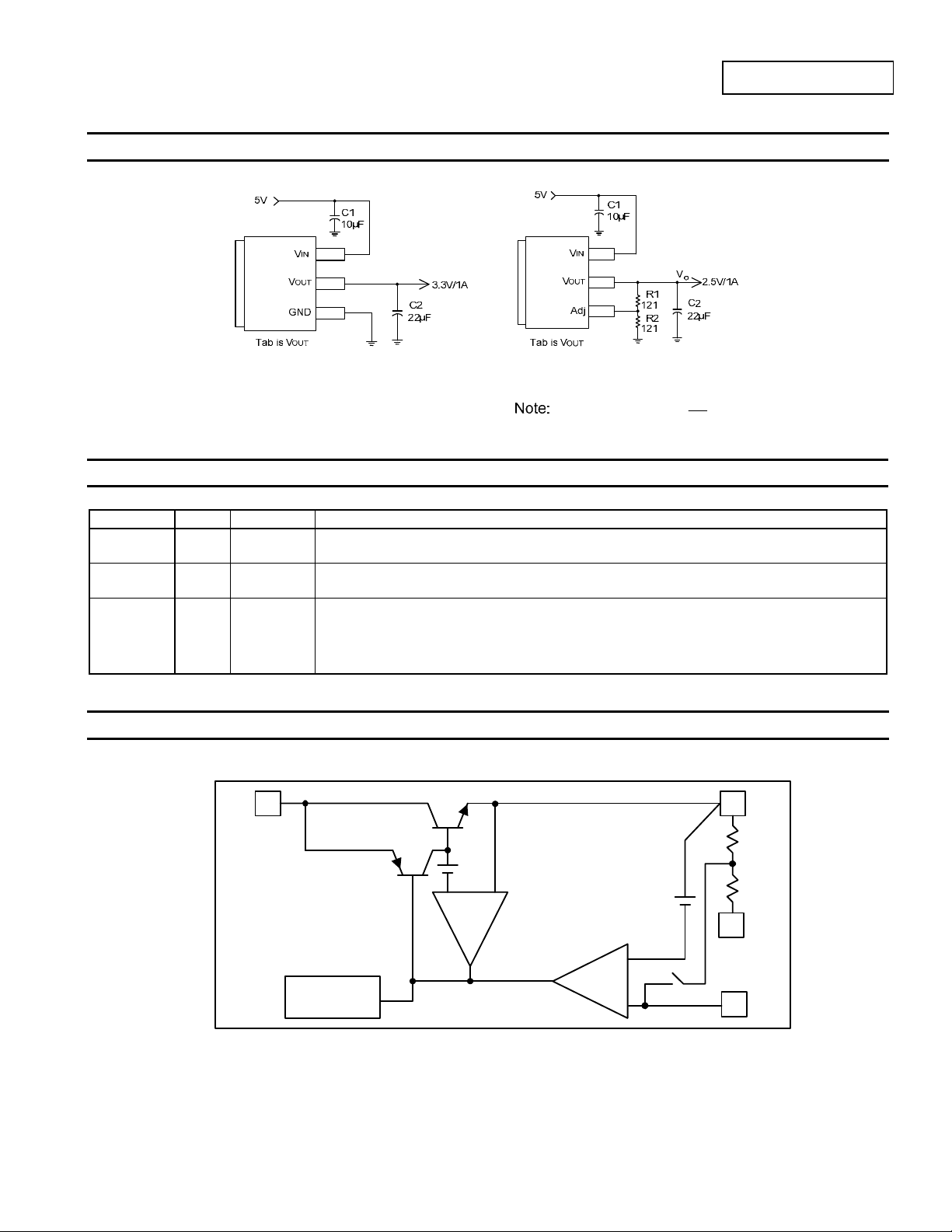
Typical Applications Circuit
AP1117/AP1117I
( 5V/3.3V fixed output )
( 5V/2.5V ADJ output )
Pin Descriptions
Pin Number I/O Pin Name Function
1 I Adj (GND)
2 O V
3 I VIN
OUT
A resistor divider from this pin to the V
Fixed-Mode).
The output of the regulator. A minimum of 4.7µF capacitor (0.15 ESR 0.5) must be connected
from this pin to ground to insure stability.
The input pin of regulator. Typically a large storage capacitor is connected from this pin to ground to
insure that the input voltage does not sag below the minimum dropout voltage during the load
transient response. This pin must always be 1.3V higher than V
properly. A minimum of 4.7µF capacitor (0.15 ESR 0.5) must be connected from this pin to
ground to insure stability.
pin and ground sets the output voltage (Ground only for
OUT
Functional Block Diagram
3
V
IN
R
2
)
(1 VV
REFo
R
1
in order for the device to regulate
OUT
2
V
OUT
AP1117/AP1117I
Document number: DS31009 Rev. 23 - 2
Thermal
Shutdown
+
+
www.diodes.com
-
CURRENT
LIMIT
2 of 13
+
1.25V
-
+
1
GND
(FIXED)
1
Adj
June 2013
© Diodes Incorporated

AP1117/AP1117I
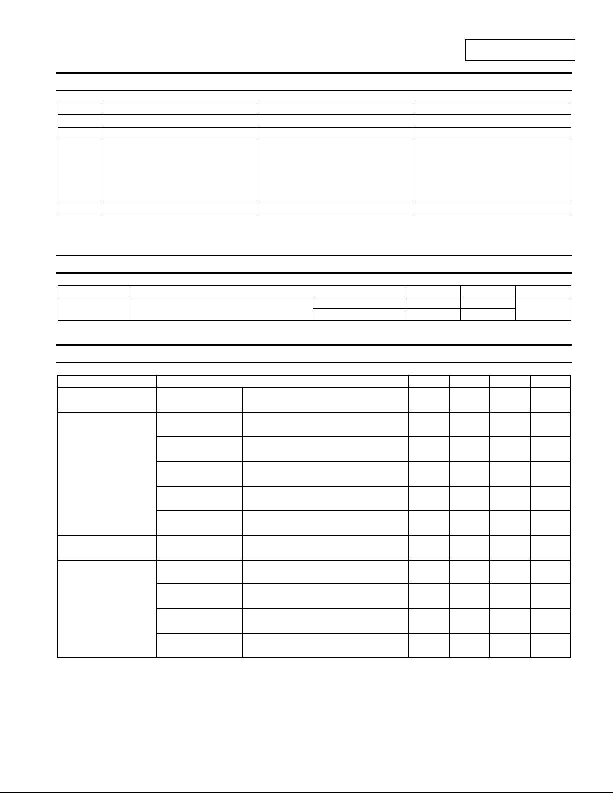
Absolute Maximum Ratings (@T
= +25°C, unless otherwise specified.)
A
Symbol Parameter Rating Unit
VIN
TMJ
DC Supply Voltage -0.3 to +18 V
Maximum Junction Temperature +150 °C
Power Dissipation
PD
SOT89-3
SOT223
TO220-3
TO252
Internally limited by maximum junction
temperature of +150°C (Note 4)
mW
TO263
TST
Notes: 4. AP1117 contains an internal thermal limiting circuit that is designed to protect the regulator in the event that the maximum junction temperature
exceeded. When activated, typically at +150°C, the regulator output switches off and then back on as the die cools
Storage Temperature -65 to +150 °C
.
Recommended Operating Conditions (@T
= +25°C, unless otherwise specified.)
A
Symbol Parameter Min Max Unit
TOP Operating Junction Temperature Range
Note: 11. 22uF is suggested for Cin/C
value when application is required to work under 0℃.
out
AP1117 0 +125
AP1117I -40 +125
°C
Electrical Characteristics (@T
= +25°C, unless otherwise specified.)
A
Parameter Conditions Min Typ Max Unit
T
= +25°C, (VIN-
Reference Voltage AP1117-ADJ
AP1117-1.5
AP1117-1.8
Output Voltage
AP1117-2.5
AP1117-3.3
AP1117-5.0
Line Regulation AP1117-XXX
AP1117-ADJ
AP1117-1.5
Load Regulation
AP1117-1.8
AP1117-2.5
Notes: 5. See thermal regulation specifications for changes in output voltage due to heating effects. Line and load regulation are measured at a constant junction
temperature by low duty cycle pulse testing. Load regulation is measured at the output lead = 1/18” from the package.
6. Line and load regulation are guaranteed up to the maximum power dissipation of 15W. Power dissipation is determined by the difference between input
and output differential and the output current. Guaranteed maximum power dissipation will not be available over the full input/output range.
A
I
= 10mA
O
= 10mA, TA = +25°C,
I
OUT
3V V
I
3.3V V
I
4V V
I
4.8V V
I
6.5V V
I
T
V
T
V
T
V
T
V
T
12V
IN
= 10mA, TA = +25°C,
OUT
12V
IN
= 10mA, TA = +25°C,
OUT
12V
IN
= 10mA, TA = +25°C,
OUT
12V
IN
= 10mA, TA = +25°C,
OUT
12V
IN
= 10mA,V
O
= 25°C
A
= 3.3V,V
IN
= +25°C (Notes 5, 6)
A
= 3V, 0mA < IO < 1A,
IN
= +25°C (Notes 5, 6)
A
= 3.3V, 0mA < IO < 1A,
IN
= +25°C (Notes 5, 6)
A
= 4V, 0mA < IO < 1A,
IN
= +25°C (Notes 5, 6)
A
) = 1.5V
OUT
+1.5V < V
OUT
= 0, 0mA < IO < 1A,
ADJ
IN
< 12V,
1.225 1.250 1.275 V
1.470 1.500 1.530 V
1.764 1.800 1.836 V
2.450 2.500 2.550 V
3.235 3.300 3.365 V
4.900 5.000 5.100 V
— — 0.2 %
— — 1 %
— 12 15 mV
— 15 18 mV
— 20 25 mV
AP1117/AP1117I
Document number: DS31009 Rev. 23 - 2
3 of 13
www.diodes.com
June 2013
© Diodes Incorporated

AP1117/AP1117I
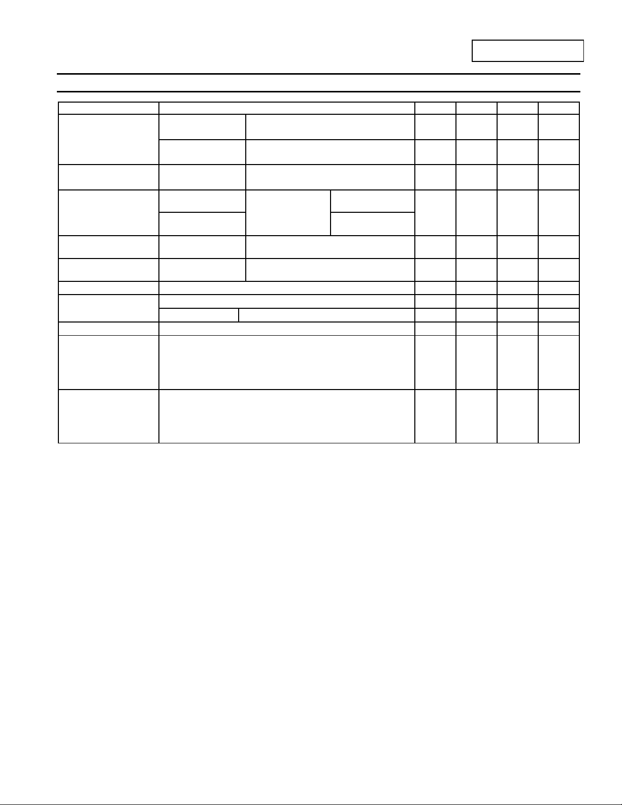
Electrical Characteristics (cont.) (@T
= +25°C, unless otherwise specified.)
A
Parameter Conditions Min Typ Max Unit
V
= 5V, 0 I
IN
T
= +25°C (Notes 5, 6)
A
V
= 8V, 0 I
IN
= +25°C (Notes 5, 6)
T
A
I
= 800mA, V
OUT
0°C T
V
OUT
Load Regulation
(cont.)
Dropout Voltage
(V
IN-VOUT
)
AP1117-3.3
AP1117-5.0
AP1117-ADJ/1.5/1.8
2.5/3.3/5.0
AP1117-ADJ/1.5/1.8
Dropout Voltage
IN-VOUT
)
(V
2.5/3.3/5.0
AP1117I-ADJ/1.5/1.8
I
OUT
V
= 1A,
OUT
= 1% V
2.5/3.3/5.0
Current Limit
Minimum Load Current
(Note 7)
Thermal Regulation
Ripple Rejection
Temperature Stability
AP1117-ADJ/1.5/1.8
2.5/3.3/5.0
AP1117-XXX
T
= +25°C, 30ms pulse
A
F = 180Hz, C
= 25µF Tantalum, I
OUT
AP1117-XXX
= 10mA
I
O
V
IN
(V
IN-VOUT
0°C T
= V
OUT
+125°C
J
+3V
SOT89-3: Control Circuitry/Power Transistor (Note 8)
Thermal Resistance
JA
Junction-to-Ambient
SOT223: Control Circuitry/Power Transistor (Note 9)
TO252: Control Circuitry/Power Transistor (Note 8)
JA
TO220-3: Control Circuitry/Power Transistor (Note 8)
TO263: Control Circuitry/Power Transistor (Note 8)
SOT89-3: Control Circuitry/Power Transistor (Note 8)
Thermal Resistance
JC
Junction-to-Case
SOT223: Control Circuitry/Power Transistor (Note 9)
TO252: Control Circuitry/Power Transistor (Note 8)
TO220-3: Control Circuitry/Power Transistor (Note 8)
TO263: Control Circuitry/Power Transistor (Note 8)
Notes: 7. Quiescent current is defined as the minimum output current required in maintaining regulation. At 12V input/output differential the device is guaranteed
to regulate if the output current is greater than 10mA.
8. Test conditions for SOT89-3, TO220-3, TO252 and TO263: Devices mounted on FR-4 substrate, single sided PC board, 2oz copper,with minimum
recommended pad layout, no air flow. The case point of
9. Test conditions for SOT223: Devices mounted on FR-4 substrate, single sided PC board, 2oz copper, with 5mm x 5mm thermal pad layout, no air flow.
The case point of
is located on the thermal tab.
JC
JC
1A,
OUT
1A,
OUT
= 1%
OUT
+125°C
J
0°C T
J
OUT
-40°C T
) = 5V
= 1A
OUT
is located on the thermal tab.
+125°C
+125°C
J
— 26 33 mV
— 40 50 mV
— 1.2 1.3 V
— 1.3 1.4 V
1. 1 — — A
— 5 10 mA
— 0.008 0.040 %/W
— — — —
— 60 70 dB
— 0.5 — %
—
—
—
—
—
—
—
—
—
—
164
107
73
78
60
42
15
12
3.5
3.5
—
—
—
—
—
—
—
—
—
—
°C/W
°C/W
AP1117/AP1117I
Document number: DS31009 Rev. 23 - 2
4 of 13
www.diodes.com
June 2013
© Diodes Incorporated
 Loading...