

Page 1
AP1117/AP1117I
1A DROPOUT POSITIVE ADJUSTABLE OR FIXED-MODE REGULATOR
Description
AP1117 is a low dropout positive adjustable or fixed-mode regulator
with 1A output current capability. The product is voltage specifically
designed to provide well-regulated supply for low IC applications such
as high-speed bus termination and low current 3.3V logic supply.
AP1117 is also well suited for other applications such as VGA cards.
AP1117 is guaranteed to have lower than 1.4V dropout at full load
current making it ideal to provide well-regulated outputs of 1.25 to 5.0
with 6.4V to 18V input supply. AP1117 is available both in commercial
temperature grade (AP1117) and in industrial temperature range
(AP1117I) (TO252 and SOT223).
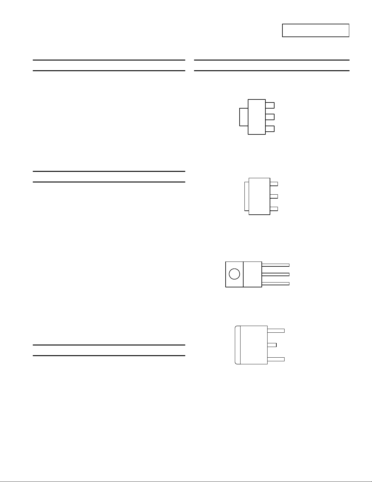
Pin Assignments
SOT89-3
( Top View )
3
2
1
Tab is V
( Top View )
OUT
SOT223
VIN
OUT
V
Adj (GND)
Features
3
VIN
1.4V Maximum Dropout at Full Load Current
Fast Transient Response
Output Current Limiting
Built-in Thermal Shutdown
Good Noise Rejection
3-Terminal Adjustable or Fixed 1.5V, 1.8V,2.5V, 3.3V, 5.0V
Operating Junction Temperature range
0°C T
-20°C T
-40°C T
Lead-Free Packages: SOT223, TO252, SOT89-3, TO263 and
TO220-3
Totally Lead-Free; RoHS Compliant (Notes 1 & 2)
SOT223, TO252, SOT89-3, TO263 and TO220-3: Available in
“Green” Molding Compound (No Br, Sb)
Halogen and Antimony Free. “Green” Device (Note 3)
+125°C (All packages)
J
+125°C (see ordering information)
J
+125°C (see ordering information)
J
( Front View )
( Top View )
2
1
Tab is V
Tab is VOUT
OUT
TO220-3
3
2
1
TO252 and TO263
3
2
VOUT
VOUT
Adj (GND)
V
IN
V
OUT
Adj (GND)
IN
V
Applications
PC Peripheral
Communication
Consumer Equipment
Notes: 1. No purposely added lead. Fully EU Directive 2002/95/EC (RoHS) & 2011/65/EU (RoHS 2) compliant.
2. See http://www.diodes.com quality/lead_free.html for more information about Diodes Incorporated’s definitions of Halogen and Antimony free, "Green"
and Lead-Free.
3. Halogen and Antimony free "Green” products are defined as those which contain <900ppm bromine, <900ppm chlorine (<1500ppm total Br + Cl) and
<1000ppm antimony compounds.
1
Tab is VOUT
Adj (GND)
AP1117/AP1117I
Document number: DS31009 Rev. 23 - 2
1 of 13
www.diodes.com
June 2013
© Diodes Incorporated
Page 2
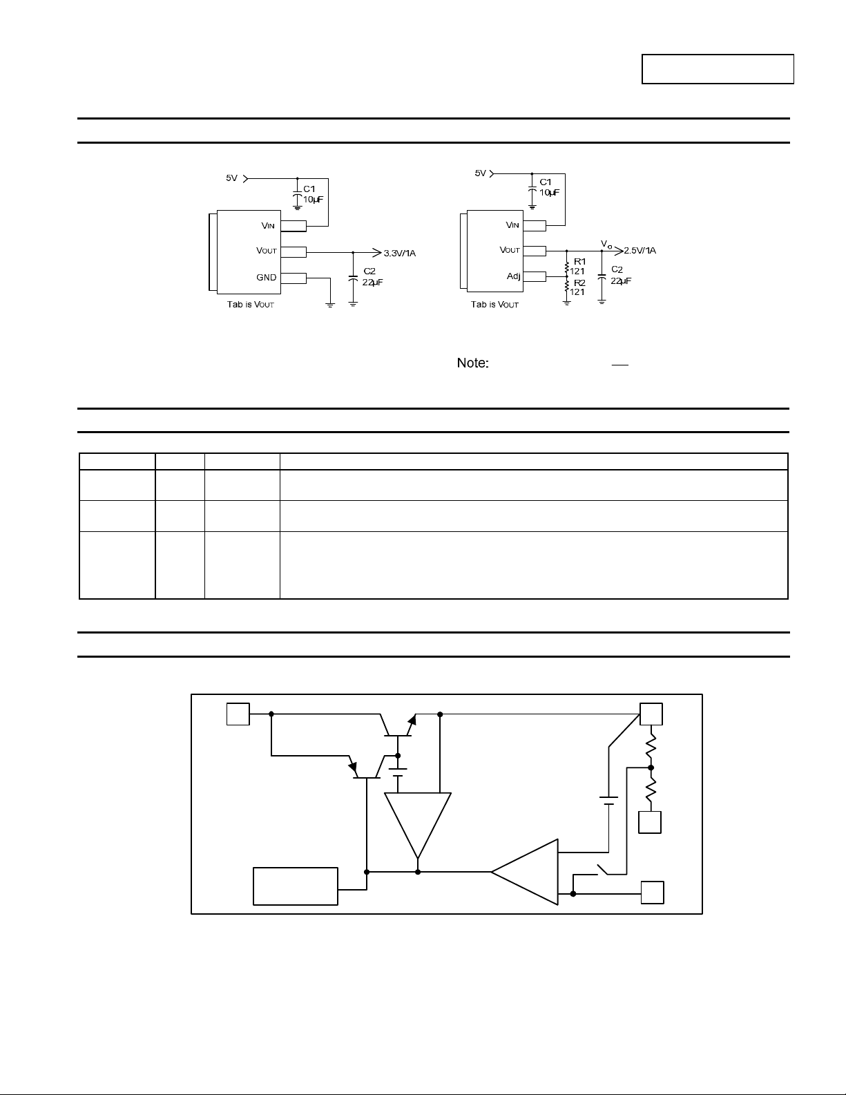
Typical Applications Circuit
AP1117/AP1117I
( 5V/3.3V fixed output )
( 5V/2.5V ADJ output )
Pin Descriptions
Pin Number I/O Pin Name Function
1 I Adj (GND)
2 O V
3 I VIN
OUT
A resistor divider from this pin to the V
Fixed-Mode).
The output of the regulator. A minimum of 4.7µF capacitor (0.15 ESR 0.5) must be connected
from this pin to ground to insure stability.
The input pin of regulator. Typically a large storage capacitor is connected from this pin to ground to
insure that the input voltage does not sag below the minimum dropout voltage during the load
transient response. This pin must always be 1.3V higher than V
properly. A minimum of 4.7µF capacitor (0.15 ESR 0.5) must be connected from this pin to
ground to insure stability.
pin and ground sets the output voltage (Ground only for
OUT
Functional Block Diagram
3
V
IN
R
2
)
(1 VV
REFo
R
1
in order for the device to regulate
OUT
2
V
OUT
AP1117/AP1117I
Document number: DS31009 Rev. 23 - 2
Thermal
Shutdown
+
+
www.diodes.com
-
CURRENT
LIMIT
2 of 13
+
1.25V
-
+
1
GND
(FIXED)
1
Adj
June 2013
© Diodes Incorporated
Page 3
AP1117/AP1117I
Absolute Maximum Ratings (@T
= +25°C, unless otherwise specified.)
A
Symbol Parameter Rating Unit
VIN
TMJ
DC Supply Voltage -0.3 to +18 V
Maximum Junction Temperature +150 °C
Power Dissipation
PD
SOT89-3
SOT223
TO220-3
TO252
Internally limited by maximum junction
temperature of +150°C (Note 4)
mW
TO263
TST
Notes: 4. AP1117 contains an internal thermal limiting circuit that is designed to protect the regulator in the event that the maximum junction temperature
exceeded. When activated, typically at +150°C, the regulator output switches off and then back on as the die cools
Storage Temperature -65 to +150 °C
.
Recommended Operating Conditions (@T
= +25°C, unless otherwise specified.)
A
Symbol Parameter Min Max Unit
TOP Operating Junction Temperature Range
Note: 11. 22uF is suggested for Cin/C
value when application is required to work under 0℃.
out
AP1117 0 +125
AP1117I -40 +125
°C
Electrical Characteristics (@T
= +25°C, unless otherwise specified.)
A
Parameter Conditions Min Typ Max Unit
T
= +25°C, (VIN-
Reference Voltage AP1117-ADJ
AP1117-1.5
AP1117-1.8
Output Voltage
AP1117-2.5
AP1117-3.3
AP1117-5.0
Line Regulation AP1117-XXX
AP1117-ADJ
AP1117-1.5
Load Regulation
AP1117-1.8
AP1117-2.5
Notes: 5. See thermal regulation specifications for changes in output voltage due to heating effects. Line and load regulation are measured at a constant junction
temperature by low duty cycle pulse testing. Load regulation is measured at the output lead = 1/18” from the package.
6. Line and load regulation are guaranteed up to the maximum power dissipation of 15W. Power dissipation is determined by the difference between input
and output differential and the output current. Guaranteed maximum power dissipation will not be available over the full input/output range.
A
I
= 10mA
O
= 10mA, TA = +25°C,
I
OUT
3V V
I
3.3V V
I
4V V
I
4.8V V
I
6.5V V
I
T
V
T
V
T
V
T
V
T
12V
IN
= 10mA, TA = +25°C,
OUT
12V
IN
= 10mA, TA = +25°C,
OUT
12V
IN
= 10mA, TA = +25°C,
OUT
12V
IN
= 10mA, TA = +25°C,
OUT
12V
IN
= 10mA,V
O
= 25°C
A
= 3.3V,V
IN
= +25°C (Notes 5, 6)
A
= 3V, 0mA < IO < 1A,
IN
= +25°C (Notes 5, 6)
A
= 3.3V, 0mA < IO < 1A,
IN
= +25°C (Notes 5, 6)
A
= 4V, 0mA < IO < 1A,
IN
= +25°C (Notes 5, 6)
A
) = 1.5V
OUT
+1.5V < V
OUT
= 0, 0mA < IO < 1A,
ADJ
IN
< 12V,
1.225 1.250 1.275 V
1.470 1.500 1.530 V
1.764 1.800 1.836 V
2.450 2.500 2.550 V
3.235 3.300 3.365 V
4.900 5.000 5.100 V
— — 0.2 %
— — 1 %
— 12 15 mV
— 15 18 mV
— 20 25 mV
AP1117/AP1117I
Document number: DS31009 Rev. 23 - 2
3 of 13
www.diodes.com
June 2013
© Diodes Incorporated
Page 4
AP1117/AP1117I
Electrical Characteristics (cont.) (@T
= +25°C, unless otherwise specified.)
A
Parameter Conditions Min Typ Max Unit
V
= 5V, 0 I
IN
T
= +25°C (Notes 5, 6)
A
V
= 8V, 0 I
IN
= +25°C (Notes 5, 6)
T
A
I
= 800mA, V
OUT
0°C T
V
OUT
Load Regulation
(cont.)
Dropout Voltage
(V
IN-VOUT
)
AP1117-3.3
AP1117-5.0
AP1117-ADJ/1.5/1.8
2.5/3.3/5.0
AP1117-ADJ/1.5/1.8
Dropout Voltage
IN-VOUT
)
(V
2.5/3.3/5.0
AP1117I-ADJ/1.5/1.8
I
OUT
V
= 1A,
OUT
= 1% V
2.5/3.3/5.0
Current Limit
Minimum Load Current
(Note 7)
Thermal Regulation
Ripple Rejection
Temperature Stability
AP1117-ADJ/1.5/1.8
2.5/3.3/5.0
AP1117-XXX
T
= +25°C, 30ms pulse
A
F = 180Hz, C
= 25µF Tantalum, I
OUT
AP1117-XXX
= 10mA
I
O
V
IN
(V
IN-VOUT
0°C T
= V
OUT
+125°C
J
+3V
SOT89-3: Control Circuitry/Power Transistor (Note 8)
Thermal Resistance
JA
Junction-to-Ambient
SOT223: Control Circuitry/Power Transistor (Note 9)
TO252: Control Circuitry/Power Transistor (Note 8)
JA
TO220-3: Control Circuitry/Power Transistor (Note 8)
TO263: Control Circuitry/Power Transistor (Note 8)
SOT89-3: Control Circuitry/Power Transistor (Note 8)
Thermal Resistance
JC
Junction-to-Case
SOT223: Control Circuitry/Power Transistor (Note 9)
TO252: Control Circuitry/Power Transistor (Note 8)
TO220-3: Control Circuitry/Power Transistor (Note 8)
TO263: Control Circuitry/Power Transistor (Note 8)
Notes: 7. Quiescent current is defined as the minimum output current required in maintaining regulation. At 12V input/output differential the device is guaranteed
to regulate if the output current is greater than 10mA.
8. Test conditions for SOT89-3, TO220-3, TO252 and TO263: Devices mounted on FR-4 substrate, single sided PC board, 2oz copper,with minimum
recommended pad layout, no air flow. The case point of
9. Test conditions for SOT223: Devices mounted on FR-4 substrate, single sided PC board, 2oz copper, with 5mm x 5mm thermal pad layout, no air flow.
The case point of
is located on the thermal tab.
JC
JC
1A,
OUT
1A,
OUT
= 1%
OUT
+125°C
J
0°C T
J
OUT
-40°C T
) = 5V
= 1A
OUT
is located on the thermal tab.
+125°C
+125°C
J
— 26 33 mV
— 40 50 mV
— 1.2 1.3 V
— 1.3 1.4 V
1. 1 — — A
— 5 10 mA
— 0.008 0.040 %/W
— — — —
— 60 70 dB
— 0.5 — %
—
—
—
—
—
—
—
—
—
—
164
107
73
78
60
42
15
12
3.5
3.5
—
—
—
—
—
—
—
—
—
—
°C/W
°C/W
AP1117/AP1117I
Document number: DS31009 Rev. 23 - 2
4 of 13
www.diodes.com
June 2013
© Diodes Incorporated
Page 5

DROPOUT VO
T
A
G
OUTP
O
A
G
A
O
OUTPU
T VOLTAG
E C
HANG
E (%
OUT
PUT VOLTAGE DE
TIO
%
O
P
O
G
O
O
A
CUR
R
A
Typical Performance Characteristics
2.0
1.8
1.6
1.4
E (V)
1.2
L
T = 25°C
J
1.0
0.8
0.6
T = 125°C
J
0.4
0.2
0
0
250 500 750 1000
OUTPUT CURRENT (mA)
Dropout V oltage vs. Output Current
2
AP1117/AP1117I
0.20
0
N (%)
TI
-0.20
E DEVI
-0.40
LT
UT V
-0.80
-1
-40 0 25 50 75 100 125
1
I = 800mA
LOAD
TEMPERATURE (°C)
Load R egulation v s. Temperature
)
1.5
1
0.5
0
-0.5
-1
)
N (
VIA
0.8
0.6
0.4
0.2
-1.5
-2
-40 -25 0 25 50 75 100 125 150
TEMPERATURE (°C)
Percent Change in Output Voltage vs. Temperature
7.5
C = 1µF
IN
C = 10µF Tantalum
OUT
6.5
N (mV)
5.5
40
E DEVIATI
20
LTA
0
INPUT VOLTAGE (V)
UT V
-20
UT
-40
0 20 40 60 80 100 120 140 160 180 200
TIME (µs)
Line Transient Resp onse
0
24
30
C = 1µF
IN
C = 10µF Tantalum
OUT
20
Preload = 100mA
10
)
0
ENT (
-10
-20
D
2
L
1
0
OUTPUT VOLTAGE DEVIATION (mV)
-1
010
6 8 10 12
INPUT VOLTAGE (V)
Line Reg ulation
20 30 40 50 60 70 80 90 100
TIME (µs)
Load Transient Response
AP1117/AP1117I
Document number: DS31009 Rev. 23 - 2
5 of 13
www.diodes.com
June 2013
© Diodes Incorporated
Page 6

AP1117/AP1117I
Application Information
Load Regulation
For improved load regulation the AP1117-ADJ should have the upper feedback resistor, R1, connected as close as possible to V
lower resistor, R2, connected as close as possible to the load GND return. This helps reduce any parasitic resistance in series with the load.
Stability and Decoupling Capacitors
Input Capacitors
To ensure stable operation, the input supply must be low impedance up to a frequency of a few MHz. This requires a closely placed input
decoupling capacitor of 4.7µF minimum. This can be either ceramic or solid tantalum. The ESR of this capacitor must be less than 0.5.
Output Capacitor
The AP1117 also requires a closely placed output capacitor as part of the device frequency compensation. As part of its improved performance
over industry standard 1117, the AP1117 is suitable for use with MLCC (Multi-Layer Ceramic Chip) capacitors. A minimum output capacitor of
4.7µF ceramic X7R or 4.7µF solid tantalum is required. Aluminum electrolytic can be used but a minimum of 47µF is required. When using
Aluminum electrolytic it is still recommended to also use a 1µF MLCC in parallel. The ESR of the output capacitors must be less than 0.5.
The AP1117 is stable when using the correct value of MLCC capacitors. When using MLCC capacitors X7R dielectric is recommended. Do not
use Y5V dielectrics.
Capacitor Track Length
Both input and output capacitors must be placed close to the AP1117. PCB traces not longer than 10mm are recommended between the
AP1117 and the capacitors.
and the
OUT
Thermal Considerations
Thermal protection circuitry will shut down the regulator should the junction temperature exceed typically +150°C at the sense point.
The AP1117 is pin compatible with similar ‘1117 regulators and offers extended temperature range and improved regulation specifications.
AP1117 series regulators have internal thermal limiting circuitry designed to protect the device during overload conditions. For continuous normal
load conditions however, the maximum junction temperature rating of +125°C must not be exceeded.
It is important to give careful consideration to all sources of thermal resistance from junction to ambient. For the SOT223 and TO252 packages,
which are designed to be surface mounted, additional heat sources mounted near the device must also be considered. Heat sinking is
accomplished using the heat spreading capability of the PCB and its copper traces. The
+12°C/W and +15°C/W respectively.
Thermal resistances from tab to ambient can be as low as 30°C/W. The total thermal resistance fro m junction to ambient (
+42 ~ +46°C/W. This requires a reasonable sized PCB with at least one layer of copper to spread the heat across the boar d and couple it into
the surrounding air. Datasheet specifications using 2 oz copper and a 5mm x 5mm pad with T
of +73°C/W and +107°C/W for TO252 and SOT223 respectively.
The thermal resistance for each application will be affected by thermal interactions with other components on the bo ard. Some experimentation
will be necessary to determine the actual value. See graphs of power dissipation and thermal pictures of different size PCB copper area fo r
guidance.
(junction to tab) of the TO252 and SOT223 are
JC
) can be as low as
JA
= +27°C, no air flow yielded JA (junction to tab)
A
AP1117/AP1117I
Document number: DS31009 Rev. 23 - 2
6 of 13
www.diodes.com
June 2013
© Diodes Incorporated
Page 7

C
X
X
AP1117/AP1117I
Ordering Information
160
150
140
130
120
/W)
110
(°
JA
100
90
80
70
60
AP1117
P vs. Copper area
D
1oz Cu on FR4
vs. Copper area
JA
1oz Cu on Fr4
4003002001000600500 800700 900
COPPER AREA (mm )
2
XX XX -
1.6
1.5
1.4
1.3
1.2
1.1
1.0
0.9
0.8
0.7
0.6
P (W)
D
Temperature Package
Blank : Commercial
I : Industrial
D : TO252
E : SOT223
K : TO263
T : TO220-3
Y : SOT89-3
V
OUT
Blank : ADJ
15 : 1.5V
18 : 1.8V
25 : 2.5V
33 : 3.3V
Lead Free Packing
L : Lead Free
G : Green
U : Tube
13 : Tape & Reel
50 : 50V
Device
Pb
AP1117DXXL-13 0 to +125°C D TO252 NA NA 2500/Tape & Reel -13
Lead-Free
AP1117DXXG-13 -20 to +125°C D TO252 NA NA 2500/Tape & Reel -13
AP1117IDXXG-13 -40 to +125°C D TO252 NA NA 2500/Tape & Reel -13
Pb
AP1117EXXL-13 0 to +125°C E SOT223 NA NA 2500/Tape & Reel -13
Lead-Free
AP1117EXXG-13 -20 to +125°C E SOT223 NA NA 2500/Tape & Reel -13
AP1117IEXXG-13 -40 to +125°C E SOT223 NA NA 2500/Tape & Reel -13
Pb
AP1117KXXL-13 0 to +125°C K TO263 NA NA 800/Tape & Reel -13
Lead-Free
AP1117KXXG-13 0 to +125°C K TO263 NA NA 800/Tape & Reel -13
Pb
AP1117TXXL-U 0 to +125°C T TO220-3 50 -U NA NA
Lead-Free
AP1117TXXG-U 0 to +125°C T TO220-3 50 -U NA NA
Pb
AP1117YXXL-13 0 to +125°C Y SOT89-3 NA NA 2500/Tape & Reel -13
Lead-Free
AP1117YXXG-13 0 to +125°C Y SOT89-3 NA NA 2500/Tape & Reel -13
Notes: 10. Pad layout as shown on Diodes Inc. suggested pad layout document AP02001, which can be found on our website at
http://www.diodes.com/datasheets/ap02001.pdf.
Note: 11. 22uF is suggested for C
Junction
Temperature
Range
/C
in
Package
Code
value when application is required to work under 0℃.
out
Packaging
(Note 10)
Quantity
Tube 13” Tape and Reel
Part
Number
Suffix
Quantity
Part Number
Suffix
AP1117/AP1117I
Document number: DS31009 Rev. 23 - 2
7 of 13
www.diodes.com
June 2013
© Diodes Incorporated
Page 8

Marking Information
(1) SOT223
AP1117/AP1117I
( Top View )
(2) TO252
Logo
Part Number
Temperature Range
Blank : Commercial I : Industrial
1117 for ADJ
: 15 for 1.5V
17-VV
18 for 1.8V
25 for 2.5V
33 for 3.3V
50 for 5.0V
1117I for ADJ
17I-VV: 15 for 1.5V
18 for 1.8V
25 for 2.5V
33 for 3.3V
50 for 5.0V
Y W X
17X-VV
Y : Year : 0~9
: Week : A~Z : 1~26 week;
W
a~z : 27~52 week;
z repersents 52 and 53 week
X : Internal code
(3) SOT89-3
Identification Code Output Version
DA AP1117-ADJ
DB AP1117-1.5V
DC AP1117-1.8V
DD AP1117-2.5V
DE AP1117-3.3V
DF AP1117-5.0V
AP1117/AP1117I
Document number: DS31009 Rev. 23 - 2
8 of 13
www.diodes.com
June 2013
© Diodes Incorporated
Page 9

Marking Information (cont.)
(4) TO263
AP1117/AP1117I
( Top View )
Logo
Part Number
VV: 15 for 1.5V
18 for 1.8V
25 for 2.5V
33 for 3.3V
50 for 5.0V
Blank for ADJ
1117-VV
YY WW X X
(5) TO220-3
( Top View )
Logo
Part Number
1117 for ADJ
17-VV : 15 for 1.5V
18 for 1.8V
25 for 2.5V
33 for 3.3V
50 for 5.0V
17 - VV
YY WW X X
Package Outline Dimensions (All dimensions in mm.)
(1) Package Typ e: SOT223
AP1117/AP1117I
Document number: DS31009 Rev. 23 - 2
A
A1
9 of 13
www.diodes.com
L : Lead Free
G : Green
YY
: Year : 01~09
WW : Week : 01~52, 52 represents
52 and 53 week
X : Internal code
L : Lead Free
G : Green
YY : Year : 01~09
WW
: Week : 01~52, 52 represents
52 and 53 week
X : Internal code
Dim Min Max Typ
SOT223
A 1.55 1.65 1.60
A1 0.010 0.15 0.05
b1 2.90 3.10 3.00
b2 0.60 0.80 0.70
C 0.20 0.30 0.25
D 6.45 6.55 6.50
E 3.45 3.55 3.50
E1 6.90 7.10 7.00
e — — 4.60
e1 — — 2.30
L 0.85 1.05 0.95
Q 0.84 0.94 0.89
All Dimensions in mm
June 2013
© Diodes Incorporated
Page 10

Package Outline Dimensions (cont.) (All dimensions in mm.)
(2) Package Type: TO252
E
b3
L3
A
c2
D
H
A2
E1
2X b2
L4
e
3X b
A1
L
a
(3) Package Type: SOT89
E
B1
D1
B
e
8° (4X)
D
(4) Package Type: TO263
L1
L2
Gauge Plane
a
E
12K
e
b2
L3
L
Detail B
AP1117/AP1117I
Document number: DS31009 Rev. 23 - 2
0
R
1
H
D
b
See Detail B
Seating
Plane
A1
0
0
2
.
L
A
7°±1°
E1
C
H
A
c2
H
c
D1
www.diodes.com
10 of 13
AP1117/AP1117I
Dim Min Max Typ
A1 0.00 0.13 0.08
A2 0.97 1.17 1.07
b2 0.76 1.14 0.95
b3 5.21 5.46 5.33
c2 0.45 0.58 0.531
D1 5.21
E1 4.32
L3 0.88 1.27 1.08
L4 0.64 1.02 0.83
Dim Min Max
A 1.40 1.60
B 0.44 0.62
B1 0.35 0.54
C 0.35 0.44
D 4.40 4.60
D1 1.62 1.83
E 2.29 2.60
e 1.50 Typ
H 3.94 4.25
H1 2.63 2.93
L 0.89 1.20
All Dimensions in mm
All Dimensions in mm
TO252
A 2.19 2.39 2.29
b 0.64 0.88 0.783
D 6.00 6.20 6.10
e
E 6.45 6.70 6.58
H 9.40 10.41 9.91
L 1.40 1.78 1.59
a 0° 10°
All Dimensions in mm
SOT89
TO263
Dim Min Max
A 4.07 4.82
A1 0.00 0.25
b 0.51 0.99
b2 1.15 1.77
c 0.356 0.73
c2 1.143 1.65
D 8.39 9.65
D1 6.55
E 9.66 10.66
E1 6.23
e 2.54 Typ
H 14.61 15.87
L 1.78 2.79
L1
L2
a 0° 8°
2.286
1.67
1.77
June 2013
© Diodes Incorporated
Page 11

Package Outline Dimensions (cont.) (All dimensions in mm.)
(5) Package Type: TO220-3
Q
D
b1
E
e
e1
ØP
D1
L1
L
b
A
F
SEATING PLANE
C
J1
Suggested Pad Layout
(1) Package Typ e: SOT223
Y1
X1
C1
(2) Package Type: TO252
AP1117/AP1117I
Document number: DS31009 Rev. 23 - 2
Y2
Y2
Y1
X2
X1
X2
E1
C2
Z
C
11 of 13
www.diodes.com
TO220-3
Dim Min Max
A 3.55 4.85
b 0.51 1.14
b1 1.14 1.78
C 0.31 1.14
D 14.20 16.50
D1 5.84 6.86
E 9.70 10.70
e 2.79 2.99
e1 4.83 5.33
F 0.51 1.40
J1 2.03 2.92
L 12.72 14.72
L1 3.66 6.35
P 3.53 4.09
Q 2.54 3.43
All Dimensions in mm
Dimensions Value (in mm)
X1 3.3
X2 1.2
Y1 1.6
Y2 1.6
C1 6.4
C2 2.3
Dimensions Value (in mm)
Z 11.6
X1 1.5
X2 7.0
Y1 2.5
Y2 7.0
C 6.9
E1 2.3
AP1117/AP1117I
June 2013
© Diodes Incorporated
Page 12

Suggested Pad Layout (cont.)
(3) Package Type: SOT89
Y3
Y
X (3x)
(4) Package Type: TO263
X
AP1117/AP1117I
Document number: DS31009 Rev. 23 - 2
X1
X2 (2x)
X1
C
Y2
AP1117/AP1117I
Dimensions Value (in mm)
X 0.900
Y1
Y4
C
Y
Y2
Y1
12 of 13
www.diodes.com
X1 1.733
X2 0.416
Y 1.300
Y1 4.600
Y2 1.475
Y3 0.950
Y4 1.125
C 1.500
Dimensions Value (in mm)
C 5.08
X
X1
Y
Y1 7.01
Y2
1.10
10.41
3.50
15.99
June 2013
© Diodes Incorporated
Page 13

AP1117/AP1117I
DIODES INCORPORATED MAKES NO WARRANTY OF ANY KIND, EXPRESS OR IMPLIED, WITH REGARDS TO THIS DOCUMENT,
INCLUDING, BUT NOT LIMITED TO, THE IMPLIED WARRANTIES OF MERCHANTABILITY AND FITNESS FOR A PARTICULAR PURPOSE
(AND THEIR EQUIVALENTS UNDER THE LAWS OF ANY JURISDICTION).
Diodes Incorporated and its subsidiaries reserve the right to make modifications, enhancements, improvements, corrections or other changes
without further notice to this document and any product described herein. Diodes Incorporated does not assume any liability arising out of the
application or use of this document or any product described herein; neither does Diodes Incorporated convey any license under its patent or
trademark rights, nor the rights of others. Any Customer or user of this document o r products described herein in such applica tions shall assume
all risks of such use and will agree to hold Diodes Incorporated and all the companies whose products are represented on Diodes Incorporated
website, harmless against all damages.
Diodes Incorporated does not warrant or accept any liability whatsoever in respect of any products purchased through unauthorized sales channel.
Should Customers purchase or use Diodes Incorporated products for any unintended or unauthorize d application, Customers shall indemnify and
hold Diodes Incorporated and its representatives harmless against all claims, damages, expenses, and attorney fees arising out of, directly or
indirectly, any claim of personal injury or death associated with such unintended or unauthorized application.
Products described herein may be covered by one or more United States, international or foreign patents pending. Product names and markings
noted herein may also be covered by one or more United States, international or foreign trademarks.
This document is written in English but may be translated into multiple languages for reference. Onl y the English version of this document is the
final and determinative format released by Diodes Incorporated.
Diodes Incorporated products are specifically not authorized for use as critical components in life support devices or systems without the express
written approval of the Chief Executive Officer of Diodes Incorporated. As used herein:
A. Life support devices or systems are devices or systems which:
1. are intended to implant into the body, or
2. support or sustain life and whose failure to perform when properly used in accordance with instructions for use provided in the
labeling can be reasonably expected to result in significant injury to the user.
B. A critical component is any component in a life support device or system whose failure to perform can be reasonably expected to cause the
failure of the life support device or to affect its safety or effectiveness.
Customers represent that they have all necessary expertise in the safety and regulatory ramifications of their life support devices or systems, and
acknowledge and agree that they are solely responsible for all legal, regulatory and safety-related requirements concerning their products and any
use of Diodes Incorporated products in such safety-critical, life support devices or systems, notwithstanding any devices- or systems-related
information or support that may be provided by Diodes Incorporated. Further, Customers must fully indemnify Diodes Incorporated and its
representatives against any damages arising out of the use of Diodes Incorporated products in such safety-critical, life support devices or systems.
Copyright © 2013, Diodes Incorporated
www.diodes.com
IMPORTANT NOTICE
LIFE SUPPORT
AP1117/AP1117I
Document number: DS31009 Rev. 23 - 2
13 of 13
www.diodes.com
June 2013
© Diodes Incorporated
 Loading...