

Page 1
Data Sheet
ADJUSTABLE PRECISION SHUNT REGULATORS AN431
General Description
The AN431 series ICs are three-terminal adjustable
shunt regulators with guaranteed thermal stability over
a full operation range. These ICs feature sharp turn-on
characteristics, low temperature coefficient and low
output impedance, which make them ideal substitutes
for Zener diodes in applications such as switching
power supply, charger and other adjustable regulators.
The output voltage of these ICs can be set to any value
between V
age (36V).
The AN431 precision reference is offered in two voltage tolerance: 0.5% and 1.0%.
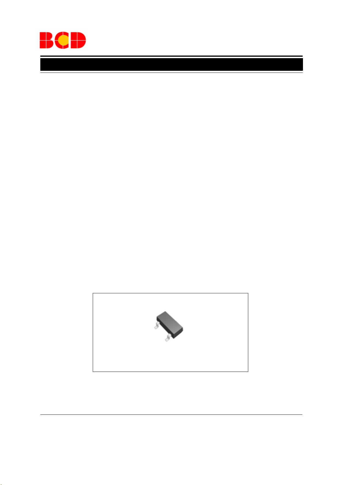
These ICs are available in SOT-23 package.
(2.5V) and the maximum cathode volt-
REF
Features
· Programmable Precise Output Voltage from 2.5V
to 36V
· High Stability under Capacitive Load
· Low Temperature Deviation: 4.5mV Typical
· Low Equivalent Full-range Temperature Coeffi-
o
cient with 20PPM/
· Low Dynamic Output Resistance: 0.15Ω Typical
· Sink Current Capacity from 1mA to 100mA
· Low Output Noise
· Wide Operating Range of -40 to 125
C Typical
o
C
Applications
· Charger
· Voltage Adapter
· Switching Power Supply
· Graphic Card
· Precision Voltage Reference
SOT-23
Figure 1. Package Type of AN431
Dec. 2012 Rev. 2. 0 BCD Semiconductor Manufacturing Limited
1
Page 2
Data Sheet
REF
V
REF
CATHODE
ANODE
+
-
3
21
ADJUSTABLE PRECISION SHUNT REGULATORS AN431
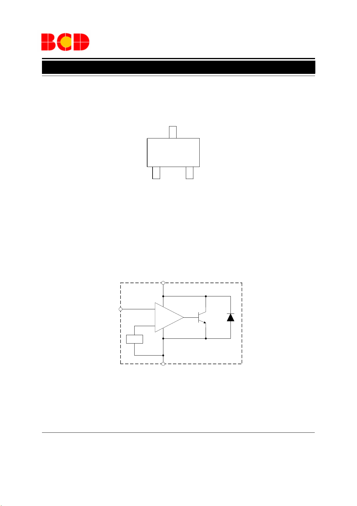
Pin Configuration
N Package
(SOT-23)
ANODE
REFCATHODE
Figure 2. Pin Configuration of AN431 (Top View)
Functional Block Diagram
2
1
3
Figure 3. Functional Block Diagram of AN431
Dec. 2012 Rev. 2. 0 BCD Semiconductor Manufacturing Limited
2
Page 3
Data Sheet
ADJUSTABLE PRECISION SHUNT REGULATORS AN431
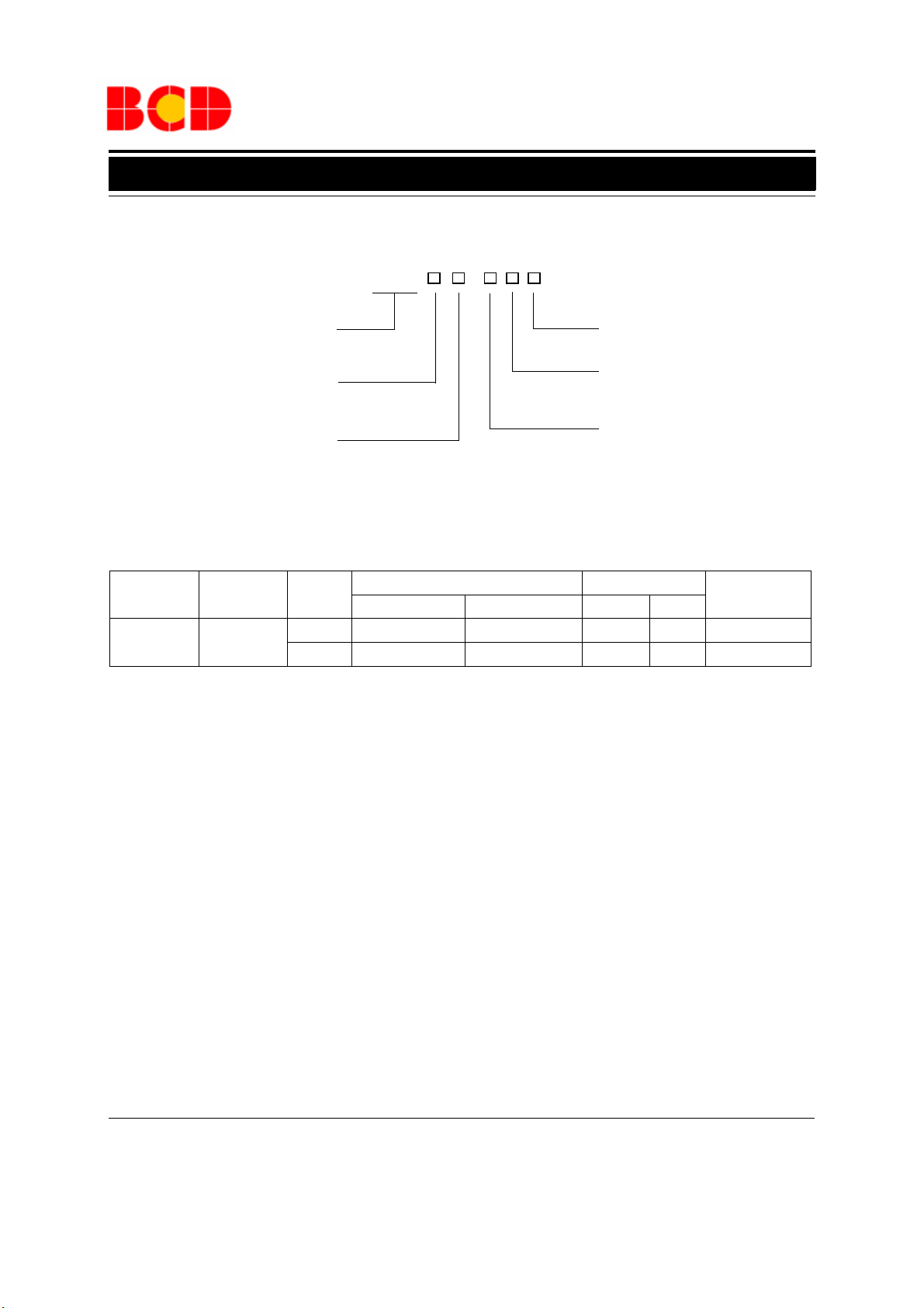
Ordering Information
AN431 -
Circuit Type
E1: Lead-Free
G1: Green
Condition
TR: Tape and Reel
A: 0.5%
B: 1.0%
Package
A: AN431 (40V)
N: SOT-23
Package
SOT-23
BCD Semiconductor's Pb-free products, as designated with "E1" suffix in the part number, are RoHS compliant. Products with
"G1" suffix are available in green packages.
Temperature
Range
-40 to
125oC
Condition
0.5% AN431AN-ATRE1 AN431AN-ATRG1 EB1 GB1 Tape & Reel
1.0%
Lead Free Green Lead Free Green
AN431BN-ATRE1 AN431BN-ATRG1 EB2 GB2 Tape & Reel
Part Number Marking ID
Packing Type
Dec. 2012 Rev. 2. 0 BCD Semiconductor Manufacturing Limited
3
Page 4
Data Sheet
ADJUSTABLE PRECISION SHUNT REGULATORS AN431
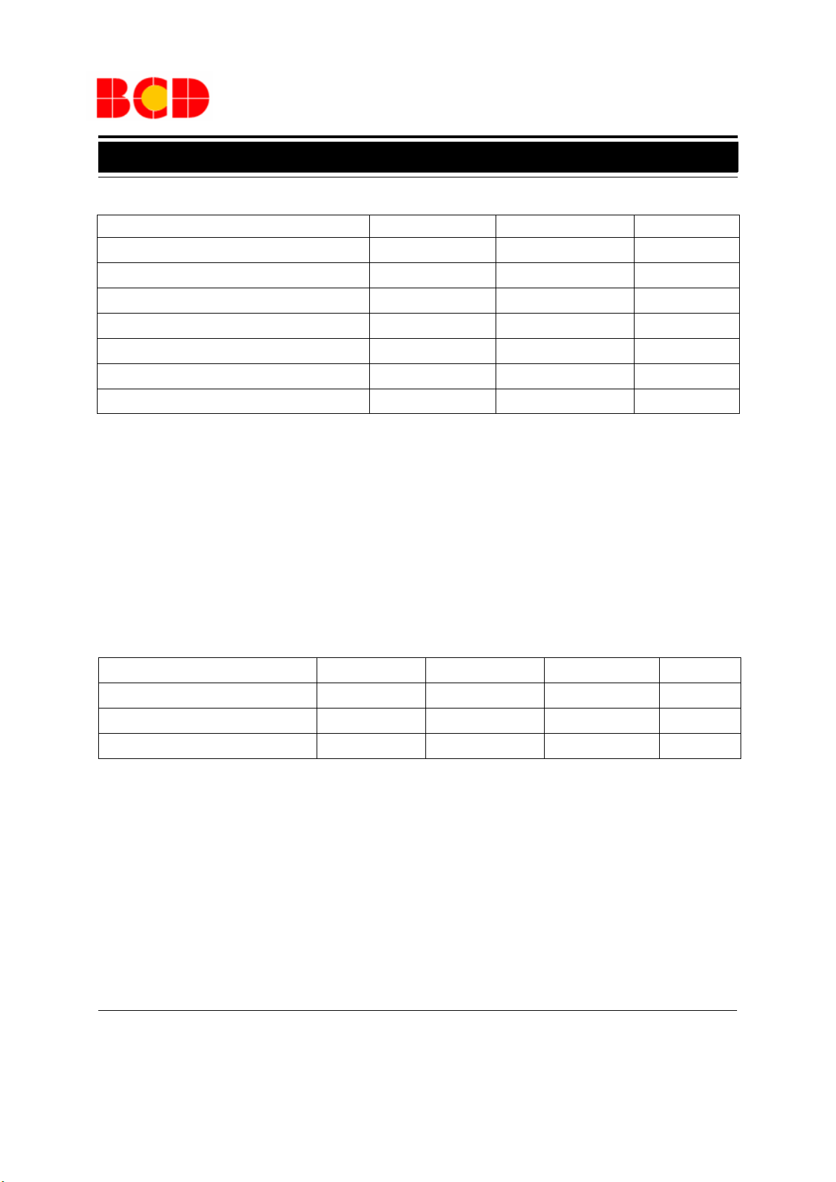
Absolute Maximum Ratings (Note 1)
Parameter Symbol Value Unit
T
V
I
I
KA
REF
P
T
STG
KA
D
40 V
-100 to 150 mA
10 mA
370 mW
J
150
-65 to 150
o
C
o
C
Cathode Voltage
Cathode Current Range (Continuous)
Reference Input Current Range
Power Dissipation
Junction Temperature
Storage Temperature Range
ESD (Human Body Model) ESD 2000 V
Note 1: Stresses greater than those listed under "Absolute Maximum Ratings" may cause permanent damage to the
device. These are stress ratings only, and functional operation of the device at these or any other conditions beyond
those indicated under "Recommended Operating Conditions" is not implied. Exposure to "Absolute Maximum
Ratings" for extended periods may affect device reliability.
Recommended Operating Conditions
Parameter Symbol Min Max Unit
Cathode Voltage
Cathode Current
V
KA
I
KA
Operating Ambient Temperature Range -40 125
Dec. 2012 Rev. 2. 0 BCD Semiconductor Manufacturing Limited
V
REF
36 V
1.0 100 mA
o
C
4
Page 5

Data Sheet
ADJUSTABLE PRECISION SHUNT REGULATORS AN431
Electrical Characteristics
Operating Conditions: TA=25oC, unless otherwise specified.
Parameter
Reference Voltage
0.5%
1.0% 2.475 2.500 2.525
Test
Circuit
Deviation of Reference Voltage Over Full Temperature Range
Ratio of Change in Reference
Voltage to the Change in
Cathode Voltage
Reference Current 5
Deviation of Reference Current
Over Full Temperature Range
Minimum Cathode Current for
Regulation
Off-state Cathode Current 6
Dynamic Impedance 4
Thermal Resistance
Symbol Conditions Min Typ Max Unit
4
4
V
ΔV
REF
REF
VKA=V
REF, IKA
VKA=V
REF
IKA=10mA
=10mA
0 to 70
-40 to 85
o
C
-40 to 125
ΔV
=
KA
ΔV
REF
5
ΔV
IKA=10mA
KA
10V to V
=
ΔV
KA
36V to 10V
I
REF
5
4
ΔI
I
(Min)
I
(Off)
Z
θ
IKA=10mA, R1=10KΩ, R2=∞
IKA=10mA, R1=10KΩ
REF
R2=∞, T
KA
V
KA=VREF
KA
V
KA
VKA=V
KA
f ≤ 1.0kHz
SOT-23 135
JC
=-40 to 125oC
A
=36V, V
REF
, IKA=1 to 100mA,
REF
=0
2.487 2.500 2.512
o
C
o
C
REF
V
4.5 8
4.5 10
mV
4.5 16
-1.0 -2.7
mV/V
-0.5 -2.0
0.7 4 μA
0.4 1.2 μA
0.4 1.0 mA
0.05 1.0 μA
0.15 0.5 Ω
o
C/W
Dec. 2012 Rev. 2. 0 BCD Semiconductor Manufacturing Limited
5
Page 6

Data Sheet
I
OFF
V
IN
V
KA
V
IN
V
KA
R1
I
KA
V
REF
V
IN
V
KA
I
KA
R1
R2
V
REF
VKA=V
REF
*(1+R1/R2)+ I
REF
*R1
I
REF
R3
ADJUSTABLE PRECISION SHUNT REGULATORS AN431
Electrical Characteristics (Continued)
Figure 4. Test Circuit 4 for VKA=V
Figure 5. Test Circuit 5 for VKA>V
REF
REF
Figure 6. Test Circuit 6 for I
OFF
Dec. 2012 Rev. 2. 0 BCD Semiconductor Manufacturing Limited
6
Page 7

Data Sheet
-60 -40 -20 0 20 40 60 80 100 120 140
0.0
0.5
1.0
1.5
R1=10K,R2=
I
KA
=10mA
Reference Current (μA)
Ambient Temperature (0C)
-60 -40 -20 0 20 40 60 80 100 120 140
2.485
2.490
2.495
2.500
2.505
2.510
Reference Voltage (V)
Ambient Temperature (oC)
VKA=V
REF
IKA=10mA
-2 -1 0 1 2 3
-100
-50
0
50
100
150
Cathode Current (mA)
Cathode Voltage (V)
VKA=V
REF
TA=250C
-1.0 -0.5 0.0 0.5 1.0 1.5 2.0 2.5
-200
0
200
400
600
800
Cathode Current (μA)
Cathode Voltage (V)
VKA=V
REF
TA=250C
ADJUSTABLE PRECISION SHUNT REGULATORS AN431
Typical Performance Characteristics
∞
Figure 7. Reference Voltage vs. Ambient Temperature Figure 8. Reference Current vs. Ambient Temperature
Figure 9. Cathode Current vs. Cathode Voltage Figure 10. Cathode Current vs. Cathode Voltage
Dec. 2012 Rev. 2. 0 BCD Semiconductor Manufacturing Limited
7
Page 8

Data Sheet
-40 -20 0 20 40 60 80 100 120
0.0
0.2
0.4
0.6
0.8
1.0
1.2
1.4
1.6
1.8
2.0
Off-state Cathode Current (μA)
Ambient Temperature (oC)
VKA=36V
V
REF
=0
-40-200 20406080100120
-1.4
-1.3
-1.2
-1.1
-1.0
-0.9
VKA=3.5V to 36V
ΔV
REF
/ ΔV
KA
(mV/V)
Ambient Temperature (oC)
10μF
8.2K
15K
I
KA
Output
242
GND
1k 10k 100k 1M
-10
0
10
20
30
40
50
60
70
Voltage Gain (dB)
Small Signal Frequency (Hz)
TA=250C
I
KA
=10mA
ADJUSTABLE PRECISION SHUNT REGULATORS AN431
Typical Performance Characteristics (Continued)
Figure 11. Off-state Cathode Current vs. Figure 12. Ratio of Delta Reference Voltage to the
Ambient Temperature
Ratio of Delta Cathode Voltage
Dec. 2012 Rev. 2. 0 BCD Semiconductor Manufacturing Limited
Figure 13. Small Signal Voltage Gain vs. Frequency
8
Page 9

Data Sheet
1K 10K 100K 1,000K
0.1
1
10
Reference Impedance (Ω)
Frequency (Hz)
IKA=10mA
T
A
=25oC
GND
Output
50
1K
I
KA
I
KA
R1 (10K)
R2
150
0
10
20
30
40
50
60
70
80
90
100
10
1
0.10.01
StableStable
Cathode Current (mA)
Load Capacitance (μF)
VKA=V
REF
VKA= 5V
VKA=10V
VKA=15V
0.001
ADJUSTABLE PRECISION SHUNT REGULATORS AN431
Typical Performance Characteristics (Continued)
Figure 14. Reference Impedance vs. Frequency
Dec. 2012 Rev. 2. 0 BCD Semiconductor Manufacturing Limited
Figure 15. Stability Boundary Conditions vs. Load Capacitance
9
Page 10

Data Sheet
Pulse
Generator
f=100KHz
220
50
Output
GND
0246
0
1
2
3
4
5
Input
Input and Output Voltage (V)
Time (μS)
Output
ADJUSTABLE PRECISION SHUNT REGULATORS AN431
Typical Performance Characteristics (Continued)
Figure 16. Pulse Response of Input and Output Voltage
Dec. 2012 Rev. 2. 0 BCD Semiconductor Manufacturing Limited
10
Page 11

Data Sheet
V
IN
V
OUT
R1
R2
V
REF
AN431
R3
V
IN V
OUT
R4
R1
R2
V
REF
R3
AN431
I
OUT
V
IN
AN431
R2
R1
ADJUSTABLE PRECISION SHUNT REGULATORS AN431
Typical Application
V
=(1+R1/R2)*V
OUT
Figure 17. Shunt Regulator
REF
Figure 18. High Current Shunt Regulator
V
=(1+R2/R3)*V
OUT
I
OUT=VREF
/R2 + I
REF
KA
Dec. 2012 Rev. 2. 0 BCD Semiconductor Manufacturing Limited
Figure 19. Current Source or Current Limit
11
Page 12

Data Sheet
AZ1117
V
IN
V
OUT
Adjust
8.2K
AN431
R1
R2
R3
250
250
5V, 1A
PWM Controller
C1
R1
R2 680
U2
3
4
PS521
C2
2
R3
R4
R5
V
OUT
AN431
Q1
COMP
VFB
ADJUSTABLE PRECISION SHUNT REGULATORS AN431
Typical Application (Continued)
Figure 20. Precision 5V 1A Regulator
Figure 21. PWM Converter with Reference
Dec. 2012 Rev. 2. 0 BCD Semiconductor Manufacturing Limited
12
Page 13

Data Sheet
2.300(0.091)
2.500(0.098)
1.200(0.047)
1.400(0.055)
0.920(0.036)
0.980(0.039)
0.300(0.012)
0.500(0.020)
1.900(0.075)REF
2.800(0.110)
3.000(0.118)
2.0°
3.0 °
0.500(0.020)
0.700(0.028)
1.050(0.041)REF
0.020(0.001)
0.100(0.004)
0.900(0.035)
1.100(0.043)
4×
R0.100(0.004)
7.0°
7.0°
0.550(0.022)REF
0.200(0.008)MIN
0.100(0.004) GAUGE PLANE
0.080(0.003)
0.150(0.006)
R0.100(0.004)
0.0°~10.0°
ADJUSTABLE PRECISION SHUNT REGULATORS AN431
Mechanical Dimensions
SOT-23 Unit: mm(inch)
Dec. 2012 Rev. 2. 0 BCD Semiconductor Manufacturing Limited
13
Page 14

BCD Semiconductor Manufacturing Limited
IMPORTANT NOTICE
IMPORTANT NOTICE
BCD Semiconductor Manufacturing Limited reserves the right to make changes without further notice to any products or specifi-
BCD Semiconductor Manufacturing Limited reserves the right to make changes without further notice to any products or specifi-
cations herein. BCD Semiconductor Manufacturing Limited does not assume any responsibility for use of any its products for any
cations herein. BCD Semiconductor Manufacturing Limited does not assume any responsibility for use of any its products for any
particular purpose, nor does BCD Semiconductor Manufacturing Limited assume any liability arising out of the application or use
particular purpose, nor does BCD Semiconductor Manufacturing Limited assume any liability arising out of the application or use
of any its products or circuits. BCD Semiconductor Manufacturing Limited does not convey any license under its patent rights or
of any its products or circuits. BCD Semiconductor Manufacturing Limited does not convey any license under its patent rights or
other rights nor the rights of others.
other rights nor the rights of others.
http://www.bcdsemi.com
MAIN SITE
MAIN SITE
- Headquarters
BCD Semiconductor Manufacturing Limited
BCD Semiconductor Manufactur ing Limited
- Wafer Fab
No. 1600, Zi Xing Road, Shanghai ZiZhu Science-based Industrial Park, 200241, China
Shanghai SIM-BCD Semiconductor Manufacturing Limited
Tel: +86-21-24162266, Fax: +86-21-24162277
800, Yi Shan Road, Shanghai 200233, China
Tel: +86-21-6485 1491, Fax: +86-21-5450 0008
REGIONAL SALES OFFICE
Shenzhen Office
REGIONAL SALES OFFICE
Shanghai SIM-BCD Semiconductor Manufacturing Co., Ltd., Shenzhen Office
Shenzhen Office
Unit A Room 1203, Skyworth Bldg., Gaoxin Ave.1.S., Nanshan District, Shenzhen,
Shanghai SIM-BCD Semiconductor Manufacturing Co., Ltd. Shenzhen Office
China
Advanced Analog Circuits (Shanghai) Corporation Shenzhen Office
Tel: +86-755-8826 7951
Room E, 5F, Noble Center, No.1006, 3rd Fuzhong Road, Futian District, Shenzhen 518026, China
Fax: +86-755-8826 7865
Tel: +86-755-8826 7951
Fax: +86-755-8826 7865
- Wafer Fab
BCD Semiconductor Manufacturing Limited
Shanghai SIM-BCD Semiconductor Manufacturing Co., Ltd.
- IC Design Group
800 Yi Shan Road, Shanghai 200233, China
Advanced Analog Circuits (Shanghai) Corporation
Tel: +86-21-6485 1491, Fax: +86-21-5450 0008
8F, Zone B, 900, Yi Shan Road, Shanghai 200233, China
Tel: +86-21-6495 9539, Fax: +86-21-6485 9673
Taiwan Office
BCD Semiconductor (Taiwan) Company Limited
Taiwan Office
4F, 298-1, Rui Guang Road, Nei-Hu District, Taipei,
BCD Semiconductor (Taiwan) Company Limited
Tai wan
4F, 298-1, Rui Guang Road, Nei-Hu District, Taipei,
Tel: +886-2-2656 2808
Taiwan
Fax: +886-2-2656 2806
Tel: +886-2-2656 2808
Fax: +886-2-2656 2806
USA Office
BCD Semiconductor Corp.
USA Office
30920 Huntwood Ave. Hayward,
BCD Semiconductor Corporation
CA 94544, USA
30920 Huntwood Ave. Hayward,
Tel : +1-510-324-2988
CA 94544, U.S.A
Fax: +1-510-324-2788
Tel : +1-510-324-2988
Fax: +1-510-324-2788
 Loading...