

Page 1
Single Phase Full-wave Motor Driver for Silent Fan Motor AM9789
Data Sheet
General Description
The AM9789 is a single-phase, full wave motor
driver suited for DC fan motor, and its speed is
controlled by PWM input signal. It is suitable for
both game machine and CPU cooler which need
silent drivers. It features lock protection, thermal
shutdown, PWM control, low noise and so on.
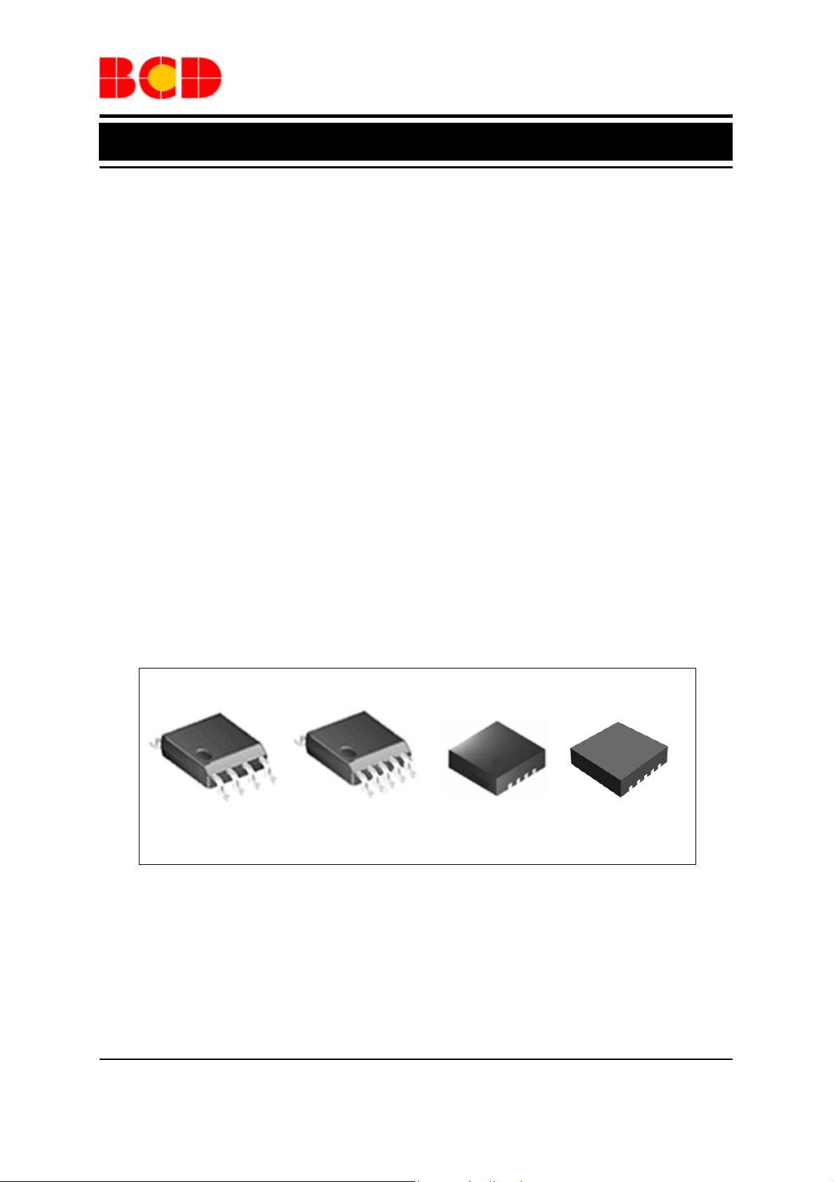
The AM9789 is available in MSOP-8, MSOP-10
DFN-3×3-8 and DFN-3×3-10 packages.
Features
• BTL Output Single-phase Full-wave Linear
Driver
• Silent Driver
• Low Supply Current (Normal Operation,Less
than 4mA)
• Low Standby Current (PWM=0 Duty) @
Supply Current Less than 200µA
• Speed Controllable by PWM Input Signal
• Built-in Quick Start Function
• Built-in Lock Protection and Auto Restart
Function
• Built-in Hall Bias Circuit
• Built-in FG Output
• Built-in Thermal Shutdown Circuit
• Built-in Over Current Protection Circuit
Applications
• Silent Fan Motors
MSOP-8 MSOP-10 DFN-3×3-8 DFN-3×3-10
Figure 1. Package Types of AM9789
Oct. 2012 Rev. 1. 1 BCD Semiconductor Manufacturing Limited
1
Page 2
Data Sheet
Single Phase Full-wave Motor Driver for Silent Fan Motor AM9789
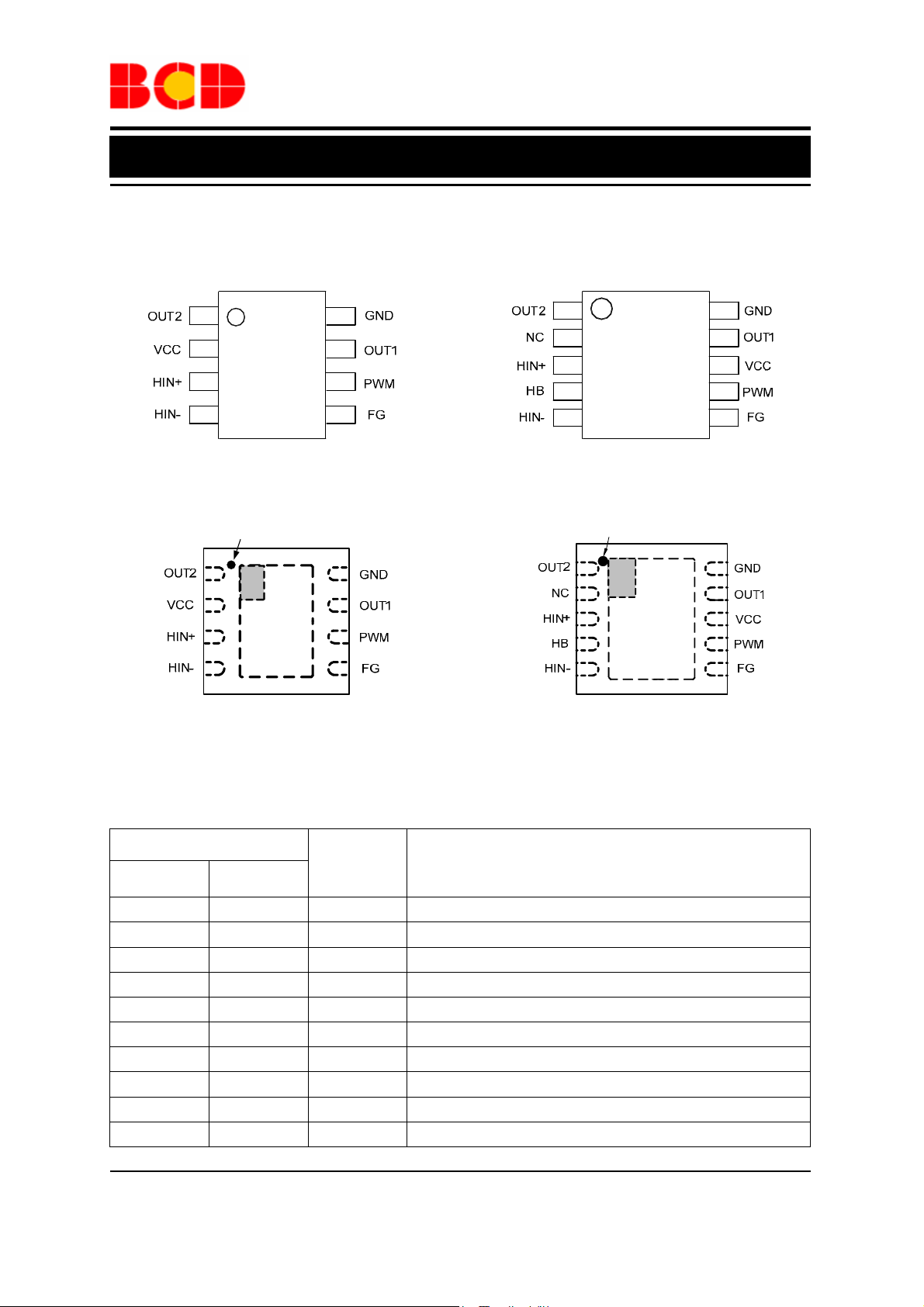
Pin Configuration
M8 Package MM Package
(MSOP-8) (MSOP-10)
1
2
3
4
DN8 Package DN Package
(DFN-3×3-8) (DFN-3×3-10)
Pin 1 Mark
1
2
3
45
Pin Description
8
7
6
5
8
7
6
1
2
3
4
5
Pin 1 Mark
1
2
3
4
56
Figure 2. Pin Configuration of AM9789 (Top View)
10
9
8
7
6
10
9
8
7
Pin Number
MSOP-10/
DFN-3×3-10
MSOP-8/
DFN-3×3-8
Pin Name Function
1 1 OUT2 Output Connection 2
2 NC No connected
3 3 HIN+ Hall input(+). Connect to Hall element positive output
4 HB Hall bias
5 4 HIN- Hall input(-). Connect to Hall element negative output
6 5 FG Rotation speed output
7 6 PWM PWM signal input terminal
8 2 VCC Power supply
9 7 OUT1 Output Connection 1
10 8 GND Ground
Oct. 2012 Rev. 1. 1 BCD Semiconductor Manufacturing Limited
2
Page 3
Data Sheet
Single Phase Full-wave Motor Driver for Silent Fan Motor AM9789
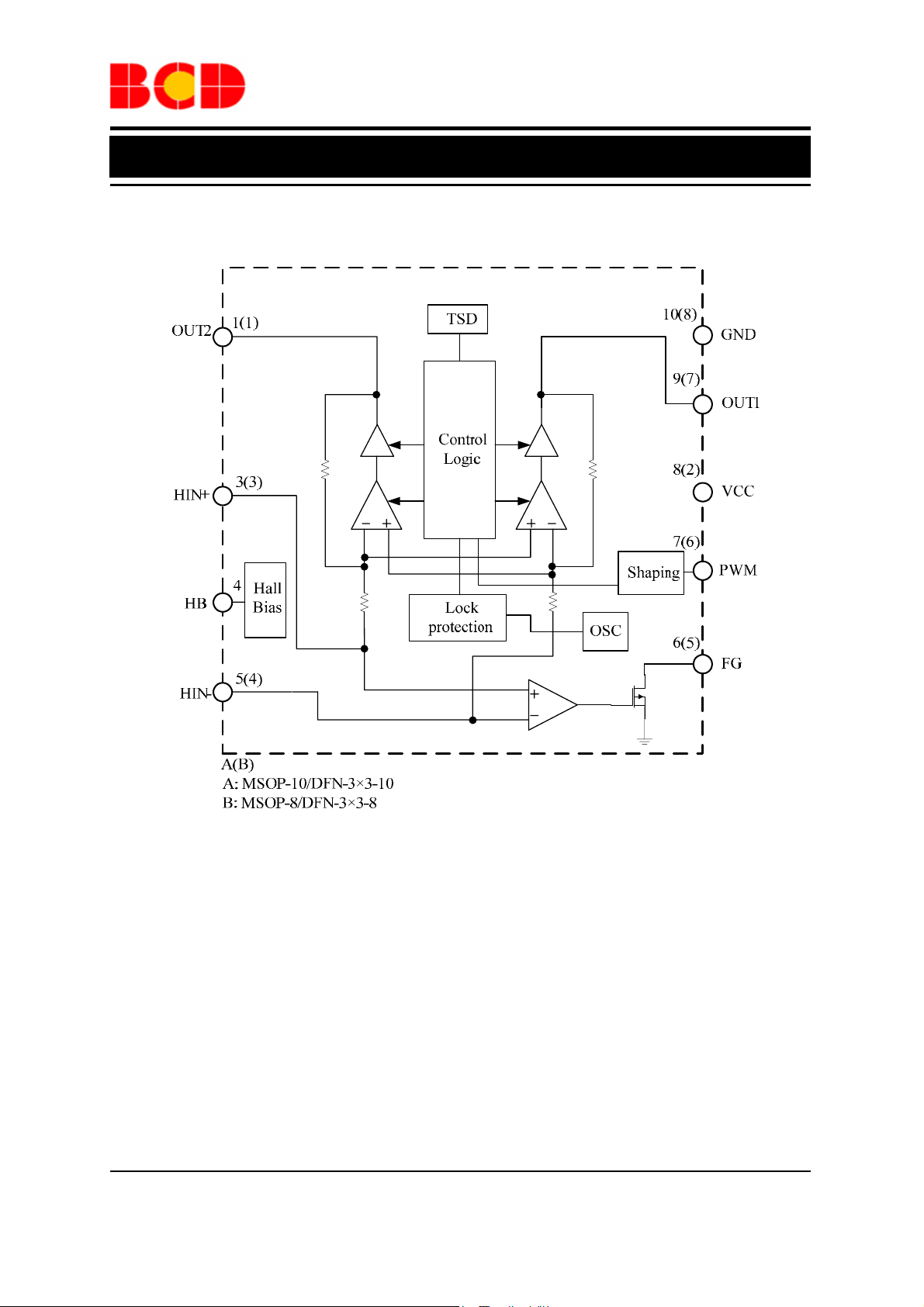
Functional Block Diagram
Figure 3. Functional Block Diagram of AM9789
Oct. 2012 Rev. 1. 1 BCD Semiconductor Manufacturing Limited
3
Page 4

Data Sheet
Single Phase Full-wave Motor Driver for Silent Fan Motor AM9789
Ordering Information
AM9789 -
Circuit Type
Package
M8: MSOP-8
MM: MSOP-10
DN8: DFN-3×3-8
DN: DFN-3×3-10
Package Temperature Range Part Number Marking ID Packing Type
G1: Green
TR: T ape & Reel
MSOP-10
MSOP-8 AM9789M8TR-G1 9789M8-G1 Tape & Reel
-40 to 105°C
DFN-3×3-8 AM9789DN8TR-G1 B6E Tape & Reel
DFN-3×3-10 AM9789DNTR-G1 BFD Tape & Reel
BCD Semiconductor's Pb-free products, as designated with "G1" suffix in the part number, are RoHS compliant
and green.
AM9789MMTR-G1 9789MM-G1 Tape & Reel
Oct. 2012 Rev. 1. 1 BCD Semiconductor Manufacturing Limited
4
Page 5

Data Sheet
Single Phase Full-wave Motor Driver for Silent Fan Motor AM9789
Absolute Maximum Ratings (TA=25°C, Note 1)
Parameter Symbol Value Unit
Supply Voltage VCC 10 V
Output Current I
Output Voltage V
HB Output Current IHB 10 mA
FG Output Voltage VFG 10 V
FG Output Sink Current IFG 10 mA
Operation T emperat ure TOP -40 to 125
Storage Temperature Range T
Lead T em perature (Soldering 10s) T
Thermal Resistance (Junction to
Ambient)
Thermal Resistance (Junction to Case)
Power Dissipation P
ESD (Human Body Model)
ESD (Machine Model)
1 A
OUT
10 V
OUT
°C
-55 to 150
STG
260
LEAD
MSOP-8 205
θ
JA
θ
JC
D
MSOP-10 195
DFN-3x3-8 71
DFN-3x3-10 71
MSOP-8 48
MSOP-10 46
DFN-3x3-8 48
DFN-3x3-10 48
MSOP-8 585
MSOP-10 585
DFN-3x3-8 1760
DFN-3x3-10 1760
4000
400
°C
°C
°C/W
°C/W
mW
V
V
Note 1: Stresses greater than those listed under “Absolute Maximum Ratings” may cause permanent damage to
the device. These are stress ratings only, and functional operation of the device at these or any other conditions
beyond those indicated under “Recommended Operating Conditions” is not implied. Exposure to “Absolute
Maximum Ratings” for extended periods may affect device reliability.
Recommended Operating Conditions (TA=25°C)
Parameter Symbol Min Max Unit
Supply Voltage VCC 2 6 V
Hall Input Voltage Range VHB 0.4 VCC -1.1 V
Operating Ambient Temperature TA -40 105
Oct. 2012 Rev. 1. 1 BCD Semiconductor Manufacturing Limited
5
°C
Page 6

Data Sheet
Single Phase Full-wave Motor Driver for Silent Fan Motor AM9789
Electrical Characteristics
V
=5V, TA=25°C, unless otherwise specified.
CC
Parameter Symbol Conditions Min Typ Max Unit
Operation Current I
Standby Current I
Rotation Mode 2 4 mA
CC1
V
CC2
=0 130 200
PWM
µA
HB Pin Output Voltage VHB IHB=5mA 1.1 1.3 1.5 V
Lock Detection ON Time tON 0.3 0.4 0.5 s
Lock Detection OFF Time t
3 4 5 s
OFF
Quick Start Enable Time tQS 55 75 ms
Output Drivers Saturation
Voltage
V
SAT(H+L)
Input-Output Gain GIO V
I
=250mA, upper
OUT
and lower total
/(V
OUT
HIN+-VHIN-
0.5 0.7 V
) 44 47 50 dB
FG Pin Low Voltage VFG IFG=5mA 0.2 0.3 V
FG Pin Leakage Current I
PWM Input High Level
Voltage
PWM Input Low Level
Voltage
PWM Input Frequency f
Hall Input Offset Voltage V
Hall Input Hysteresis
Voltage
Thermal Protection
Temperature
Thermal Hysteresis Width
VFG=5V 0.1 1
FGL
V
PWMH
V
PWML
PWM
V
T
△T
HOFS
HYS
SD
SD
0.5×V
CC
V
V
CC
0 0.2×VCC V
0.02 50 kHz
±10 mV
±5 ±10 ±15 mV
165
30
µA
°C
°C
Oct. 2012 Rev. 1. 1 BCD Semiconductor Manufacturing Limited
6
Page 7

Data Sheet
Single Phase Full-wave Motor Driver for Silent Fan Motor AM9789
Typical Performance Characteristics
4.0
3.5
Operation Mode
3.0
V
PWM=VCC
2.5
2.0
1.5
Supply Current (mA)
1.0
0.5
0.0
0123456
Supply Voltage (V)
200
150
100
Supply Current (µA)
50
0
0123456
Standby Mode
V
PWM
=0V
Supply Voltage (V)
Figure 4. Supply Current vs. Supply Voltage (V
PWM=VCC
) Figure 5. Supply Current vs. Supply Voltage (V
PWM
800
600
V
SAT-H
V
SAT-L
400
200
Saturation Voltage (mV)
0
0 100 200 300 400 500
Output Current (mA)
800
700
600
500
400
300
Power Dissipation (mW)
200
100
0
-40 -20 0 20 40 60 80 100 120 140
Ambient Temperature (oC)
Figure 6. Saturation Voltage vs. Output Current Figure 7. Power Dissipation vs. Temperature (MSOP)
Package: MSOP-10/MSOP-8
=0V)
Oct. 2012 Rev. 1. 1 BCD Semiconductor Manufacturing Limited
7
Page 8

Data Sheet
Single Phase Full-wave Motor Driver for Silent Fan Motor AM9789
Typical Performance Characteristics (Continued)
2000
1500
Package: DFN-3x 3-10/DFN-3x3-8
1000
500
Power Dissipation (mW)
0
-40 -20 0 20 40 60 80 100 120 140
Ambient Temperature (oC)
Figure 8. Power Dissipation vs. Temperature (DFN)
Oct. 2012 Rev. 1. 1 BCD Semiconductor Manufacturing Limited
8
Page 9

Data Sheet
Single Phase Full-wave Motor Driver for Silent Fan Motor AM9789
Truth Table
INPUT OUTPUT
HIN- HIN+ PWM OUT1 OUT2 FG
L H
H L L H OFF
H L
L H L L L
L H
H L L L OFF
- -
H
L
-
L OFF OFF OFF Standby Mode
H L L
L L OFF
L L OFF
Mode
Operation Mode
Lock Mode
Oct. 2012 Rev. 1. 1 BCD Semiconductor Manufacturing Limited
9
Page 10

Data Sheet
Single Phase Full-wave Motor Driver for Silent Fan Motor AM9789
T ypical Application
For MSOP-10 package
Oct. 2012 Rev. 1. 1 BCD Semiconductor Manufacturing Limited
10
Page 11

Data Sheet
Single Phase Full-wave Motor Driver for Silent Fan Motor AM9789
T ypical Application (Continued)
For MSOP-8 package
Figure 9. Typical Applications of AM9789 (Note 2)
Note 2:
D1 is an ordinary diode used to filter the noise from VCC and protect IC if VCC and GND are plugged reversed.
C1=1µF/10V typical.
R1 and R2 should be fine tuned based on system design. They can be removed according to the system
requirements.
Zener diode (D2) is an optional choice.
R
=10kΩ typical.
FG
Oct. 2012 Rev. 1. 1 BCD Semiconductor Manufacturing Limited
11
Page 12

5V/div
Data Sheet
Single Phase Full-wave Motor Driver for Silent Fan Motor AM9789
Application Information
1. Reverse Connection of Power Supply
Connector
Reverse connection of power supply connector may
break IC. Some methods such as inserting a diode
between power supply and VCC terminal can be
taken to avoid the reverse connection destruction.
2. Power Supply Line
Back electromotive force (EMF) causes regenerated
current to the power supply line, so insert a capacitor
(recommended value: 1µF or larger) as close as
possible to the space between the power supply pin
(VCC pin) and ground pin (GND pin) for routing
regenerated current.
3. GND Potential and External Components
Ensure that the potential of GND terminal is the
minimum potential in any operating condition.
External components connected to the ground must
be connected with lines that are as short as possible
and external components connected between IC pins
must be placed as close to the pins as possible.
4. Mounting Failures
In the process of attaching IC to the printed board,
more attention must be paid to the direction and
location of the IC, since mounting failures may also
break IC. In addition, destruction is also possible
when the circuit is shorted by foreign substance
between outputs or between output and power supply
or between output and GND.
5. Thermal Consideration
Refer to Figure 7 “Power Dissipation vs. Ambient
Temperature (MSOP-10/MSOP-8)”, the IC is safe to
operate below the curve and the thermal protection
will be caused if the operating area is above the line.
For example, when T
dissipation is about 0.35W.
The power dissipation can be calculated by the
following equation:
P
D=VSAT(H+L)×IOUT+VCC×ICC
For example, VCC=5V, ICC=2mA, I
V
SAT(H+L)
The GND pin provides an electrical connection to the
ground and channeling heat away. The printed circuit
board (PCB) forms a heat sink and dissipates most of
Oct. 2012 Rev. 1. 1 BCD Semiconductor Manufacturing Limited
=75°C, the maximum power
A
=0.5V, then PD=0.135W.
=250mA,
OUT
the heat to the ambient air.
6. Thermal Shutdown Circuit
Considering the power dissipation under actual
operating condition, the thermal design must be
applied with sufficient margin.
AM9789 features thermal shutdown (TSD) circuit
(operation temperature is 165°C typical and
hysteresis width is 30°C typical). When the chip
temperature reaches the TSD circuit temperature, the
output terminal becomes an open state. TSD circuit is
designed simply for the purpose of intercepting IC
from overheating. Make sure that the IC should not
be used again after this circuit operating. Figure 10
shows a fan rotates normally first and then enters into
OTP mode since the chip temperature reaches 165°C.
Finally the chip temperature decreases below 135°C,
then OTP mode is canceled and the fan rotates
normally again.
V
OUT1
5V/div
V
OUT2
V
FG
5V/div
Time 1s/div
Figure 10. OTP Function
7. Over Current Protection
The driver current is detected by AM9789 internal
circuit. When the output current is over 1A or larger,
AM9789 will close the output driver. After that if the
output current decreases, AM9789 will enable the fan
to rotate again. Figure 11 shows the detailed process.
V
OUT1
5V/div
V
OUT2
5V/div
V
FG
5V/div
Time 1s/div
Figure 11. OCP Function
8. PWM Mode
The output transistor is on when a high-level voltage
is input to the PWM pin, and is off when a low-level
voltage is input. PWM controls the speed of the
motor by inputting the pulse in accordance with the
duty cycle to the PWM pin. When the motor is
12
Page 13

Data Sheet
Single Phase Full-wave Motor Driver for Silent Fan Motor AM9789
V
Application Information
(Continued)
operated with the PWM pin open, the built-in resistor
enables the PWM pin to change to high-level voltage
and the motor speed rises to full speed. When the
PWM pin is fixed at low-level voltage, the motor
decelerates, and after the motor stops, it enters
“Power Saving Mode”. Figure 12 shows a rotating
fan’s waveform at PWM Mode. Figure 13 shows
Lock Mode Waveform at PWM input condition in the
same fan.
V
OUT1
5V/div
V
OUT2
5V/div
V
FG
5V/div
IIN
200mA/div
Figure 12. PWM Mode Waveform
(PWM: 50% duty cycle, V
V
OUT1
5V/div
V
OUT2
5V/div
VFG
5V/div
200mA/div
I
IN
Figure 13. Lock Mode at PWM Input Condition
(PWM: 50% duty cycle, V
9. Frequency Generator Function
The FG pin is an open collector output, connecting a
pull-up resistor to a high level voltage for the
frequency generator function. During the lock mode,
FG pin output will be always high. Open the terminal
when not in use. Figure 14 shows how this function
works.
Oct. 2012 Rev. 1. 1 BCD Semiconductor Manufacturing Limited
Time 10ms/div
=5V, VL=0V)
H
Time 2s/div
=5V, VL=0V)
H
OUT1
2V/div
V
OUT2
2V/div
V
FG
2V/div
I
200mA/div
IN
Figure 14. Rotation Mode Waveform
Time 2ms/div
10. Lock Protection and Auto-restart
The IC detects the rotation of the motor by Hall
signal and the lock detection ON time (t
time (t
) are adjusted by the internal counter. As
OFF
) and OFF
ON
showed below.
V
OUT1
2V/div
V
OUT2
2V/div
V
FG
2V/div
I
IN
200mA/div
Figure 15. Lock Mode Waveform
Time 2s/div
11. Quick Start and Standby Mode
The IC will enter standby mode when PWM input
keeps low level for more than 55ms (typ.). In standby
mode, shutdown amplifier and FG will be shutdown,
and the supply current is around 130µA. In standby
mode, the lock protection function doesn’t work; the
fan will restart when released from standby mode.
Figure 16 describes this function.
Figure 16. Quick Start and Standby Mode
13
Page 14

Data Sheet
Single Phase Full-wave Motor Driver for Silent Fan Motor AM9789
Mechanical Dimensions
MSOP-10 Unit: mm(inch)
)
)
7
9
8
9
1
1
.
.
0
0
(
(
0
0
5
5
7
0
.
.
4
5
Note: Eject hole, oriented hole and mold mark is optional.
Oct. 2012 Rev. 1. 1 BCD Semiconductor Manufacturing Limited
0.180(0.007)
0.280(0.011)
2.900(0.114)
3.100(0.122)
0.500(0.020)
TYP
)
1
0
0
.
0
(
0
2
0
.
0
0
0
3
2
.
0
)
)
4
2
1
2
1
1
.
.
0
0
(
(
0
0
0
0.400(0.016)
0.800(0.031)
)
6
0
0
.
0
(
0
5
1
.
0
14
0
9
1
.
.
2
3
0
°
°
6
)
9
0
0
.
0
(
5
0
(
0
.
0
3
0
0
.
7
9
5
0
0
.
0
.
8
2
0
1
.
1
0
0
)
)
(
0
.
0
3
7
.
0
3
2
)
(
0
(
0
.
0
4
3
)
)
4
0
0
.
0
(
0
9
0
.
Page 15

Data Sheet
Single Phase Full-wave Motor Driver for Silent Fan Motor AM9789
Mechanical Dimensions (Continued)
MSOP-8 Unit: mm(inch)
4.700(0.185)
5.100(0.201)
Note: Eject hole, oriented hole and mold mark is optional.
Oct. 2012 Rev. 1. 1 BCD Semiconductor Manufacturing Limited
0.300(0.012)TYP
0.650(0.026)TYP
2.900(0.114)
3.100(0.122)
`
P
Y
T
)
6
0
0
.
0
(
0
5
1
.
0
)
)
4
2
1
2
1
1
.
.
0
0
(
(
0
0
0
0.410(0.016)
0.650(0.026)
)
)
8
0
0
0
0
0
.
.
0
0
(
(
0
0
0
0
0
2
.
.
0
0
15
0
9
1
.
.
2
3
0
°
6
°
(
0
.
0
3
0
0
.
7
6
0
0
.
9
7
0
0
0
.
8
0
1
.
2
0
0
)
3
8
)
(
0
.
0
(
0
.
0
3
1
)
.
0
4
7
)
(
0
Page 16

Data Sheet
Single Phase Full-wave Motor Driver for Silent Fan Motor AM9789
Mechanical Dimensions (Continued)
DFN-3×3-8 Unit: mm(inch)
2.900(0.114)
3.100(0.122)
Pin 1 Mark
2.900(0.114)
3.100(0.122)
1.400(0.055)
1.600(0.063)
0.153(0.006)
0.253(0.010)
0.700(0.028)
0.800(0.031)
0.000(0.000)
0.050(0.002)
Oct. 2012 Rev. 1. 1 BCD Semiconductor Manufacturing Limited
16
0.180(0.007)
0.300(0.012)
N5
N4
0
5
0
6
.
0
(
.
6
0
)
2
C
S
B
N8
N1
DETAIL A
12
12 12
Pin 1 options
0.375(0.015)
0.575(0.023)
2.
(0.087 )
200
2.400(0.094)
PIN #1 IDENTIFICATION
See DETAIL A
Page 17

Data Sheet
Single Phase Full-wave Motor Driver for Silent Fan Motor AM9789
Mechanical Dimensions (Continued)
DFN-3×3-10 Unit: mm(inch)
0.700(0.028)
0.800(0.031)
2.900(0.114)
3.100(0.122)
Pin 1 Mark
0.000(0.000)
0.050(0.002)
2.900(0.114)
3.100(0.122)
1.600(0.063)
1.800(0.071)
0.200(0.008)
0.300(0.012)
0.500(0.020)
TYP
N6 N10
2.300(0.090)
2.500(0.098)
N5
0.300(0.012)
0.500(0.020)
N1
DETAIL A
PIN #
1 IDENTIFICATION
See DETAIL A
0.153(0.006)
0.253(0.010)
12
12 12
Pin 1 options
Oct. 2012 Rev. 1. 1 BCD Semiconductor Manufacturing Limited
17
Page 18

BCD Semiconductor Manufacturing Limited
IMPORTANT NOTICE
IMPORTANT NOTICE
BCD Semiconductor Manufacturing Limited reserves the right to make changes without further notice to any products or specifi-
BCD Semiconductor Manufacturing Limited reserves the right to make changes without further notice to any products or specifi-
cations herein. BCD Semiconductor Manufacturing Limited does not assume any responsibility for use of any its products for any
cations herein. BCD Semiconductor Manufacturing Limited does not assume any responsibility for use of any its products for any
particular purpose, nor does BCD Semiconductor Manufacturing Limited assume any liability arising out of the application or use
particular purpose, nor does BCD Semiconductor Manufacturing Limited assume any liability arising out of the application or use
of any its products or circuits. BCD Semiconductor Manufacturing Limited does not convey any license under its patent rights or
of any its products or circuits. BCD Semiconductor Manufacturing Limited does not convey any license under its patent rights or
other rights nor the rights of others.
other rights nor the rights of others.
http://www.bcdsemi.com
MAIN SITE
MAIN SITE
- Headquarters
BCD Semiconductor Manufacturing Limited
BCD Semiconductor Manufactur ing Limited
- Wafer Fab
No. 1600, Zi Xing Road, Shanghai ZiZhu Science-based Industrial Park, 200241, China
Shanghai SIM-BCD Semiconductor Manufacturing Limited
Tel: +86-21-24162266, Fax: +86-21-24162277
800, Yi Shan Road, Shanghai 200233, China
Tel: +86-21-6485 1491, Fax: +86-21-5450 0008
REGIONAL SALES OFFICE
Shenzhen Office
REGIONAL SALES OFFICE
Shanghai SIM-BCD Semiconductor Manufacturing Co., Ltd., Shenzhen Office
Shenzhen Office
Unit A Room 1203, Skyworth Bldg., Gaoxin Ave.1.S., Nanshan District, Shenzhen,
Shanghai SIM-BCD Semiconductor Manufacturing Co., Ltd. Shenzhen Office
China
Advanced Analog Circuits (Shanghai) Corporation Shenzhen Office
Tel: +86-755-8826 7951
Room E, 5F, Noble Center, No.1006, 3rd Fuzhong Road, Futian District, Shenzhen 518026, China
Fax: +86-755-8826 7865
Tel: +86-755-8826 7951
Fax: +86-755-8826 7865
- Wafer Fab
BCD Semiconductor Manufacturing Limited
Shanghai SIM-BCD Semiconductor Manufacturing Co., Ltd.
- IC Design Group
800 Yi Shan Road, Shanghai 200233, China
Advanced Analog Circuits (Shanghai) Corporation
Tel: +86-21-6485 1491, Fax: +86-21-5450 0008
8F, Zone B, 900, Yi Shan Road, Shanghai 200233, China
Tel: +86-21-6495 9539, Fax: +86-21-6485 9673
Taiwan Office
BCD Semiconductor (Taiwan) Company Limited
Taiwan Office
4F, 298-1, Rui Guang Road, Nei-Hu District, Taipei,
BCD Semiconductor (Taiwan) Company Limited
Tai wan
4F, 298-1, Rui Guang Road, Nei-Hu District, Taipei,
Tel: +886-2-2656 2808
Taiwan
Fax: +886-2-2656 2806
Tel: +886-2-2656 2808
Fax: +886-2-2656 2806
USA Office
BCD Semiconductor Corp.
USA Office
30920 Huntwood Ave. Hayward,
BCD Semiconductor Corporation
CA 94544, USA
30920 Huntwood Ave. Hayward,
Tel : +1-510-324-2988
CA 94544, U.S.A
Fax: +1-510-324-2788
Tel : +1-510-324-2988
Fax: +1-510-324-2788
 Loading...