

Page 1
Data Sheet
ADJUSTABLE-SPEED SINGLE-PHASE FULL-WAVE PRE-DRIVER FOR MOTOR AM4967
General Description
The AM4967 is a single-coil, single-phase motor predriver designed by bipolar process. Its rotation speed
can be controlled through an external PWM. This IC
requires few external components and has the merit of
high efficiency which make it suitable for use in great
air volume, large current and high voltage applications.
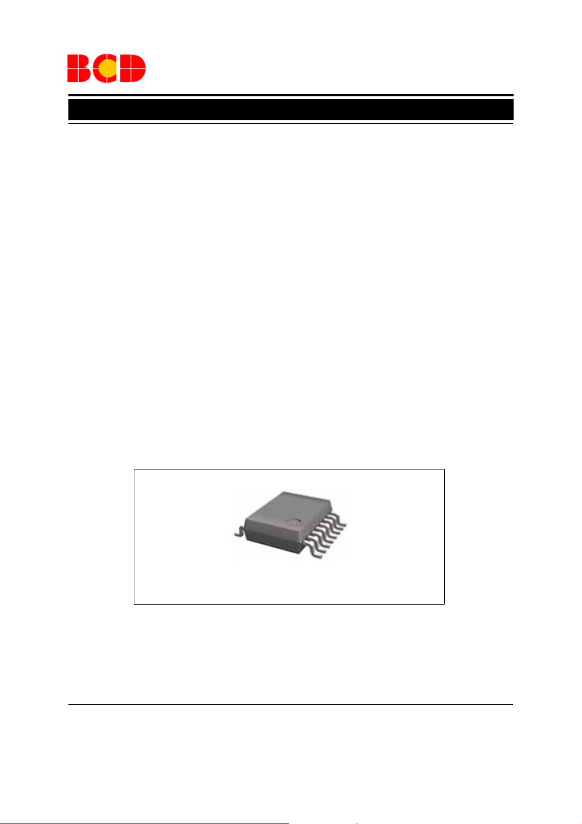
The AM4967 is available in SSOP-16 package.
Features
· Single-phase Full-wave Pre-drive
· Rotation Speed Control via External PWM
· Maximum Operating Current Limit
· Linear Start Function for Reducing Large Current
Impulse at the Moment of Turn-on
· Minimum Rotation Speed Setting
· Lock Protection and Auto Start Function
· Rotation Speed Indication
· Over Temperature Protection
Application
· CPU and OA (Office Automation) Cooler Fan
· Brushless DC Motor
SSOP-16
Figure 1. Package Type of AM4967
Oct. 2008 Rev. 1. 2 BCD Semiconductor Manufacturing Limited
1
Page 2
Data Sheet
ADJUSTABLE-SPEED SINGLE-PHASE FULL-WAVE PRE-DRIVER FOR MOTOR AM4967
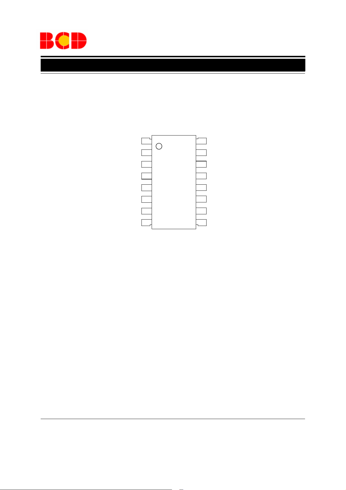
Pin Configuration
GS Package
(SSOP-16)
OUT2
OUT2B
VCC
CS
VMIN
VPWM
COSC
FG/RD
1
2
3
4
5
6
7
8
16
15
14
13
12
11
HIN+
10
9
OUT1
OUT1B
GND
VREF
LS
CT
HIN-
Figure 2. Pin Configuration of AM4967
Oct. 2008 Rev. 1. 2 BCD Semiconductor Manufacturing Limited
2
Page 3

Data Sheet
ADJUSTABLE-SPEED SINGLE-PHASE FULL-WAVE PRE-DRIVER FOR MOTOR AM4967
Pin Description
Pin Number Pin Name Function
1 OUT2
2 OUT2B
3 VCC Power supply
4CS
5VMIN
6VPWM
7COSC
8FG/RD
9HIN-
10 HIN+
11 CT
12 LS
Second channel P-type driver output. Open-drain output, must be connected
with pull-up resistor to drive external power devices in operation
Second channel N-type driver output. Push-pull output to drive external
power devices
Current limiter indicator. Fixed to 0.2V internally. Maximum allowable current is decided by external sample resistance. When the voltage of this pin
exceeds 0.2V, the output will be shut down by current limit. If this function is
not used, connect this pin to ground directly
Minimum speed setting terminal. Connect it to VREF whe n disused. In case it
is tied to other power supply for controlling, an isolated resistor is necessary
Speed control terminal. It is full speed mode when connected to ground. If the
speed is controlled by PWM mode, the frequency of control signal is 20kHz
to 100kHz. Moreover, a low pass network is necessary to transfer PWM to
DC level
PWM basic oscillation frequency generator when connected with a capacitor
of 220pF. 30kHz frequency is available.
"FG" means pin 8 is an output pin of FG signal which is used for detecting
rotation speed. "RD" means pin 8 is an output pin of RD signal, and is used
for detecting fan rotate-stop state. "FG" and "RD" can be selected according
to the requirement. This pin need to be connected with pull-up resistor when
used. A new pulse will be generated once input signal changed. Keep this pin
open when it is not to be used
Hall sensor negative input. To prevent noise, this pin is recommended to be
placed as close as possible to Hall circuit. If necessary, a capacitor may be
added between HIN+ and HIN- to reduce the influence caused by noise
Hall sensor positive input. To avoid noise, this pin is recommended to be
placed as close as possible to Hall circuit
Lock protection and auto start frequency generator. It is connected with an
external 0.47µF capacitor which decides lock-rotate time and start time. If
lock-rotate protection function is disused, please connect this pin to GND
Linear start terminal. This pin is connected to VREF externally via a capacitor
of 0.47µF to 1µF which enables fan start steadily. Start time is dependent to
the capacitance. If linear start function is not used, connect this pin to ground
13 VREF 5V voltage reference
14 GND Ground for circuit control
15 OUT1B
16 OUT1
Oct. 2008 Rev. 1. 2
First channel N-type driver output. Push-pull output to drive external power
devices
First channel P-type driver output. Open-drain output, must be connected with
pull-up resistor to drive external power devices in operation
BCD Semiconductor Manufacturing Limited
3
Page 4
Data Sheet
ADJUSTABLE-SPEED SINGLE-PHASE FULL-WAVE PRE-DRIVER FOR MOTOR AM4967
Functional Block Diagram
8
15
16
FG/RD
OUT1B
OUT1
2
OUT2B
1
OUT2
CT
VCC
VREF
HIN+
HIN-
11
3
13
10
9
Lock Shutdown
Auto Restart
5V
Reference
Hysteresis
Amp
and
Controller
Thermal Shutdown
Pre-
driver
Hysteresis
Amp
Oscillation
12
LS
67
5
VPWM
VMIN
COSC
4
CS GND
Figure 3. Functional Block Diagram of AM4967
14
Oct. 2008 Rev. 1. 2 BCD Semiconductor Manufacturing Limited
4
Page 5
Data Sheet
ADJUSTABLE-SPEED SINGLE-PHASE FULL-WAVE PRE-DRIVER FOR MOTOR AM4967
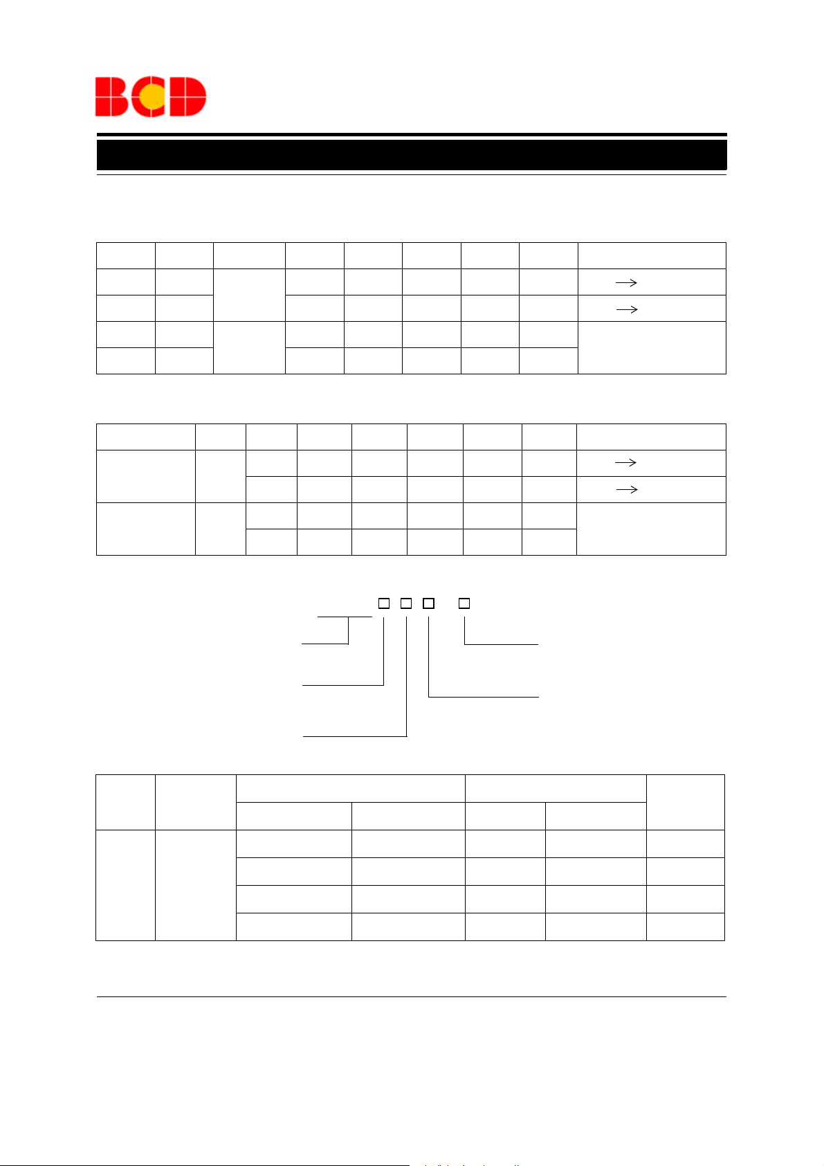
Truth Table
1. Driver-lock. V
HIN- HIN+ CT OUT1 OUT1B OUT2 OUT2B FG/RD Mode
HL
L H OFF H L L OFF OUT2 OUT1 (Driver)
HL
L H OFF H OFF L OFF
is High, V
OSC
L
H
, V
PWM
L L OFF H L OUT1 OUT2 (Driver)
OFF L OFF H L
and VLS are low.
VMIN
Lock Protection
2. Speed control. VCT, VLS are low.
VPWM, VMIN COSC HIN- HIN+ OUT1 OUT1B OUT2 OUT2B Mode
H L L L OFF H OUT1 OUT2 (Driver)
LH
HL
L H OFF H L L OUT2 OUT1 (Driver)
HLOFFLOFFH
LHOFFHOFFL
Regenerative
Ordering Information
AM4967 -
Circuit Type
E1: Lead Free
G1: Green
Pin 8
R: RD
Blank: FG
TR: Tape and Reel
Blank: Tube
Package
GS: SSOP-16
Package
SSOP-16
BCD Semiconductor's Pb-free products, as designated with "E1" suffix in the part number, are RoHS compliant. Products with
"G1" suffix are available in green package.
Temperature
Range
-30 to 105
o
Lead Free Green Lead Free Green
AM4967GS-E1 AM4967GS-G1 AM4967GS AM4967GS-G1 Tube
AM4967GSTR-E1 AM4967GSTR-G1 AM4967GS AM4967GS-G1 Tape & Reel
C
AM4967RGS-E1 AM4967RGS-G1 AM4967RGS AM4967RGS-G1 Tube
AM4967RGSTR-E1 AM4967RGSTR-G1 AM4967RGS AM4967RGS-G1 Tape & Reel
Oct. 2008 Rev. 1. 2
Part Number Marking ID
BCD Semiconductor Manufacturing Limited
Packing
Type
5
Page 6

Data Sheet
ADJUSTABLE-SPEED SINGLE-PHASE FULL-WAVE PRE-DRIVER FOR MOTOR AM4967
Absolute Maximum Ratings (Note 1)
Parameter Symbol Value Unit
Supply Voltage V
OUT1B/OUT2B Output Current I
OUTB
OUT1/OUT2 Sink Current I
OUT1B/OUT2B/OUT1/OUT2
V
Withstand Voltage
VPWM/VMIN Withstand Voltage V
PWM/VVMIN
LS Withstand Voltage V
FG/RD Withstand Voltage V
FG/RD Output Current I
FG/VRD
FG/IRD
VREF Output Current I
Power Dissipation (Note 2) P
Storage Temperature Range T
CC
OUT
OUT
LS
REF
D
STG
18 V
20 mA
20 mA
18 V
7V
7V
V
CC
V
10 mA
20 mA
800 mW
-55 to 150
o
C
ESD (Human Body Model) ESD 2000 V
Note 1: Stresses greater than those listed under "Absolute Maximum Ratings" may cause permanent damage to the device.
These are stress ratings only, and functional operation of the device at these or any other conditions beyond those indicated
under "Recommended Operating Conditions" is not implied. Exposure to "Absolute Maximum Ratings" for extended periods
may affect device reliability.
Note 2: When mounted on the specified printed circuit board (114.3mm
×76.1mm×1.6mm, glass epoxy).
Recommended Operating Conditions
Parameter Symbol Min Typ Max Unit
Supply Voltage V
CC
VPWM/VMIN Input Voltage 0 5 V
Hall Input Voltage 0.2 3 V
Ambient Temperature T
A
5.5 16 V
-30 105
o
C
Oct. 2008 Rev. 1. 2 BCD Semiconductor Manufacturing Limited
6
Page 7

Data Sheet
ADJUSTABLE-SPEED SINGLE-PHASE FULL-WAVE PRE-DRIVER FOR MOTOR AM4967
Electrical Characteristics
(VCC=12V, TA=25oC, unless otherwise specified.)
Parameter Symbol Conditions Min Typ Max Unit
Quiescent Current
VREF Reference Voltage
Current Limit Voltage
COSC High Level Voltage
COSC Low Level Voltage
COSC Frequency
CT High Level Voltage
CT Low Level Voltage
CT Charge Current
CT Discharge Current
CT Charge and Discharge Ratio
Linear Start Charge Current
OUT1B/OUT2B High Level Voltage
OUT1B/OUT2B Low Level Voltage
I
I
V
V
V
V
f
V
V
I
I
R
I
V
V
Q1
Q2
REF
LIM
OSCH
OSCL
OSC
CTH
CTL
CHG
DHG
CD
LS
OBH
OBL
Lock off 8 10 12
Lock on 8 10 12
I
OUT
=5mA
4.5 5.0 5.5 V
186 200 215
3.0 3.4 3.8 V
0.9 1.1 1.3 V
CL=220pF
25.4 30 35.5 kHz
2.4 3.3 3.6 V
1.0 1.3 1.6 V
VCT=0.5V
VCT=3.5V
I
CHG/IDHG
VLS=1V
I
=10mA VCC-
OUT
I
=10mA
OUT
1.5 2 2.5 µA
0.13 0.2 0.25 µA
8.5 10 14.5
0.5 0.7 µA
VCC-
1.8
0.9
V
CC
0.9 1.5 V
mA
mV
V
OUT1/OUT2 Low Level Vol ta g e
FG Signal Hall Input Sensitivity
FG Saturation Voltage
FG Leakage Current
VPWM/VMIN Bias Current
Oct. 2008 Rev. 1. 2
I
V
V
OL
HN
=10mA
OUT
I
HIN+, IHIN-
difference voltage
(include offset and hysteresis)
I
V
SAT
I
LFG
I
PWMB/IVMINBVOSC=VPWM/VVMIN
SINK
VFG=V
=5mA
CC
BCD Semiconductor Manufacturing Limited
7
=2V
0.45 0.8 V
±10 mV
200 500 mV
30 µA
0.1 3 µA
Page 8

Data Sheet
ADJUSTABLE-SPEED SINGLE-PHASE FULL-WAVE PRE-DRIVER FOR MOTOR AM4967
Typical Performance Characteristics
16
14
12
10
8
Supply Current (mA)
6
4
2 4 6 8 1012141618
Supply Voltage (V)
TA=25°C
Figure 4. Supply Current vs. Supply Voltage
16
14
12
10
8
6
Supply Current (mA)
4
2
0
-40-30-20-100 1020304050607080
Ambient Temperature (OC)
VCC=12V
Figure 5. Supply Current vs. Ambient Temperature
6.0
5.5
5.0
4.5
Reference Voltage (V)
4.0
3.5
-40-30-20-100 102030405060708090
Ambient Temperature (OC)
Figure 6.
Reference Voltage
vs. Ambient Temperature
VCC=12V
I
=5mA
OUT
7.5
7.0
6.5
6.0
5.5
5.0
4.5
4.0
Reference Voltage (V)
3.5
3.0
2.5
0 2 4 6 8 101214161820
Output Current (mA)
Figure 7. Reference Voltage
vs. Output Current
VCC=12V
TA=25OC
Oct. 2008 Rev. 1. 2 BCD Semiconductor Manufacturing Limited
8
Page 9

Data Sheet
ADJUSTABLE-SPEED SINGLE-PHASE FULL-WAVE PRE-DRIVER FOR MOTOR AM4967
Typical Performance Characteristics (Continued)
1000
800
600
400
Power Dissipation (mW)
200
0
-20 0 20 40 60 80 100
Ambient Temperature (°C)
Figure 8. Power Dissipation vs. Ambient Temperature
Oct. 2008 Rev. 1. 2
BCD Semiconductor Manufacturing Limited
9
Page 10

Data Sheet
ADJUSTABLE-SPEED SINGLE-PHASE FULL-WAVE PRE-DRIVER FOR MOTOR AM4967
Operating Diagram
VPWM Voltage
VMIN Voltage
COSC Voltage
0V
FG
f
=30kHz (C
OSC
ON-Duty-Small
Minimum Speed Setup
Rotation (Stop Mode)
OSC
Low
Speed
=220pF)
PWM Adjustable
Speed
ON-Duty-Large
High
Speed
3.0V
1.0V
Full Speed
RPM
Figure 9. Operating Diagram 1 of AM4967 (Speed Control, Note 3)
Note 3:
1. Minimum Speed Setting Mode (Stop Mode)
When fan rotate at low speed, its lowest speed is settable
by VMIN pin voltage. If not, fan motor stops.
2. Low Speed to High Speed Setting Mode
PWM control system works by comparing the voltage of
VPWM and COSC (1.0V to 3.0V). When VPWM voltage
is low, the transistors of the upper and lower side outputs
are ON. On contrary, when VPWM voltage is high, the
upper side transistors are OFF. And coil current re-circulates in a lower side transistor. Therefore, as the VPWM
voltage becomes lower, output ON duty becomes large.
Sequentially, coil current increases and the motor runs at
high speed which is monitored by FG output while rotation-stop state is monitored by RD output.
3. Full Speed Rotation Mode
When VPWM voltage drops to 1.0V or lower, motor fan
will run at full speed. (If the speed is not controlled,
=GND)
V
PWM
Oct. 2008 Rev. 1. 2 BCD Semiconductor Manufacturing Limited
10
Page 11

Data Sheet
ADJUSTABLE-SPEED SINGLE-PHASE FULL-WAVE PRE-DRIVER FOR MOTOR AM4967
Operating Diagram (Continued)
LS Voltage
3.0V
VMIN Voltage
COSC
VPWM Voltage
0V
Lock Protection Linear Start VPWM Setting Speed
100%
ON-Duty
0%
Figure 10. Operating Diagram 2 of AM4967 (Linear Start, VPWM Voltage<VMIN Voltage, Note 4)
1.0V
VPWM Voltage
VMIN Voltage
LS Voltage
3.0V
COSC
1.0V
0V
Lock Protection Linear
Start
100%
VMIN Setting Speed
ON-Duty
0%
Figure 11. Operating Diagram 3 of AM4967 (Linear Start, VPWM Voltage>VMIN Voltage, Note 4)
Oct. 2008 Rev. 1. 2 BCD Semiconductor Manufacturing Limited
11
Page 12

Data Sheet
ADJUSTABLE-SPEED SINGLE-PHASE FULL-WAVE PRE-DRIVER FOR MOTOR AM4967
Operating Diagram (Continued)
VPWM Voltage
VMIN Voltage
0V
Lock Protection
RD
High Level Low Level
100%
ON-Duty
0%
LS Voltage
Linear
Start
3.0V
COSC
1.0V
VMIN Setting Speed
Figure 12. Operating Diagram 4 of AM4967 (Note 4)
Note 4: The inclination of LS voltage is adjusted between V
to be 0.1µF to 1.0µF.
LS
and V
according to the capacitance which is recommended
REF
Oct. 2008 Rev. 1. 2 BCD Semiconductor Manufacturing Limited
12
Page 13

Data Sheet
ADJUSTABLE-SPEED SINGLE-PHASE FULL-WAVE PRE-DRIVER FOR MOTOR AM4967
Typical Application
Power In
PWM In
More than
1µF/25V
More than
1µF/25V
Hall
OUT1 OUT2
13
VREF
9
HIN-
10
HIN+
12
LS
5
VMIN
6
VPWM
3
VCC
AM4967
OUT1B
OUT2B
FG/RD
CS
OUT1
OUT2
GND
1kΩ
100Ω
10kΩ~
100kΩ
8
4
16
15
1
2
14
Oct. 2008 Rev. 1. 2
220pF
(f=30kHz)
COSC
7
11
CT
0.47µF
Figure 13. Typical Application of AM4967 (VCC=12V)
BCD Semiconductor Manufacturing Limited
13
Page 14

Data Sheet
ADJUSTABLE-SPEED SINGLE-PHASE FULL-WAVE PRE-DRIVER FOR MOTOR AM4967
Mechanical Dimensions
SSOP-16 Unit: mm(inch)
3.800(0.150)
4.000(0.157)
0.800(0.031)
Φ
0.900(0.035)1.000(0.039)
0.200(0.008)
0.300(0.012)
0.635(0.025)
BSC
0.100(0.004)
0.250(0.010)
o
7
o
7
4.700(0.185)
5.100(0.201)
1.350(0.053)
1.750(0.069)
0.400(0.016)
5.800(0.228)
6.200(0.244)
o
8
o
8
0.200(0.008)
0.250(0.010)
0.650(0.026)
0.750(0.030)
SEE
DETAIL A
0.150(0.006)
0.250(0.010)
1.350(0.053)
1.550(0.061)
1.270(0.050)
R0.150(0.006)
0.020(0.001)
0.050(0.002)
o
0
o
8
DETAIL A
0.250(0.010)
R0.150(0.006)
Oct. 2008 Rev. 1. 2 BCD Semiconductor Manufacturing Limited
14
Page 15

BCD Semiconductor Manufacturing Limited
IMPORTANT NOTICE
IMPORTANT NOTICE
BCD Semiconductor Manufacturing Limited reserves the right to make changes without further notice to any products or specifi-
BCD Semiconductor Manufacturing Limited reserves the right to make changes without further notice to any products or specifi-
cations herein. BCD Semiconductor Manufacturing Limited does not assume any responsibility for use of any its products for any
cations herein. BCD Semiconductor Manufacturing Limited does not assume any responsibility for use of any its products for any
particular purpose, nor does BCD Semiconductor Manufacturing Limited assume any liability arising out of the application or use
particular purpose, nor does BCD Semiconductor Manufacturing Limited assume any liability arising out of the application or use
of any its products or circuits. BCD Semiconductor Manufacturing Limited does not convey any license under its patent rights or
of any its products or circuits. BCD Semiconductor Manufacturing Limited does not convey any license under its patent rights or
other rights nor the rights of others.
other rights nor the rights of others.
http://www.bcdsemi.com
MAIN SITE
MAIN SITE
- Headquarters
BCD Semiconductor Manufacturing Limited
BCD Semiconductor Manufactur ing Limited
- Wafer Fab
No. 1600, Zi Xing Road, Shanghai ZiZhu Science-based Industrial Park, 200241, China
Shanghai SIM-BCD Semiconductor Manufacturing Limited
Tel: +86-21-24162266, Fax: +86-21-24162277
800, Yi Shan Road, Shanghai 200233, China
Tel: +86-21-6485 1491, Fax: +86-21-5450 0008
REGIONAL SALES OFFICE
Shenzhen Office
REGIONAL SALES OFFICE
Shanghai SIM-BCD Semiconductor Manufacturing Co., Ltd., Shenzhen Office
Shenzhen Office
Unit A Room 1203, Skyworth Bldg., Gaoxin Ave.1.S., Nanshan District, Shenzhen,
Shanghai SIM-BCD Semiconductor Manufacturing Co., Ltd. Shenzhen Office
China
Advanced Analog Circuits (Shanghai) Corporation Shenzhen Office
Tel: +86-755-8826 7951
Room E, 5F, Noble Center, No.1006, 3rd Fuzhong Road, Futian District, Shenzhen 518026, China
Fax: +86-755-8826 7865
Tel: +86-755-8826 7951
Fax: +86-755-8826 7865
- Wafer Fab
BCD Semiconductor Manufacturing Limited
Shanghai SIM-BCD Semiconductor Manufacturing Co., Ltd.
- IC Design Group
800 Yi Shan Road, Shanghai 200233, China
Advanced Analog Circuits (Shanghai) Corporation
Tel: +86-21-6485 1491, Fax: +86-21-5450 0008
8F, Zone B, 900, Yi Shan Road, Shanghai 200233, China
Tel: +86-21-6495 9539, Fax: +86-21-6485 9673
Taiwan Office
BCD Semiconductor (Taiwan) Company Limited
Taiwan Office
4F, 298-1, Rui Guang Road, Nei-Hu District, Taipei,
BCD Semiconductor (Taiwan) Company Limited
Tai wan
4F, 298-1, Rui Guang Road, Nei-Hu District, Taipei,
Tel: +886-2-2656 2808
Taiwan
Fax: +886-2-2656 2806
Tel: +886-2-2656 2808
Fax: +886-2-2656 2806
USA Office
BCD Semiconductor Corp.
USA Office
30920 Huntwood Ave. Hayward,
BCD Semiconductor Corporation
CA 94544, USA
30920 Huntwood Ave. Hayward,
Tel : +1-510-324-2988
CA 94544, U.S.A
Fax: +1-510-324-2788
Tel : +1-510-324-2988
Fax: +1-510-324-2788
 Loading...