

Page 1
SINGLE PHASE FULL WAVE DIRECT PWM MOTOR DRIVER AM4962
Data Sheet
General Description
The AM4962 is a full wave driver IC with direct
PWM control function. It is used for single phase
motor and is capable of speed control by PWM pulse.
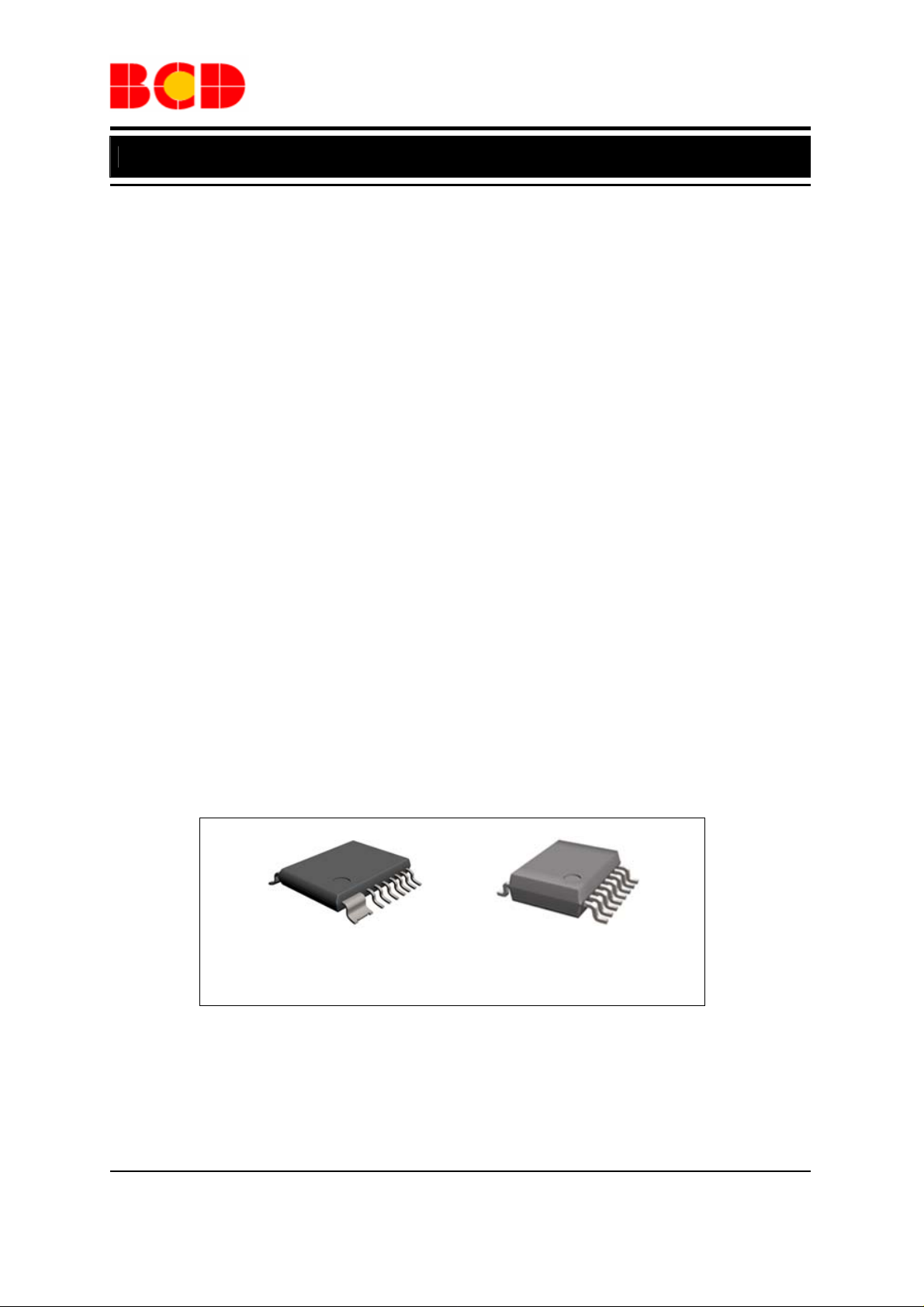
The AM4962 is available in HTSSOP-14 and
SSOP-16 packages.
Features
The Motor Speed is Controlled by PWM Pulse
•
Directly
• Built-in Triangle Wave Circuit Without Extra
Oscillation Capacitor
• Built-in Hall Bias Circuit
• Built-in Minimal Speed Setup Circuit
• Slope K* Adjustable
• Rotation Speed Indication (FG)
• Rotation or Lock State Indication (RD)
• Built-in Thermal Shutdown Circuit
• Lock Protection and Auto-restart
• Output Current Limit
* Slope K is the slope of output PWM duty vs. input
PWM duty
Applications
• CPU Cooler Fan in PC
• Brushless DC Motor Driver
HTSSOP-14 SSOP-16
Figure 1. Package Types of AM4962
Apr. 2011 Rev. 1. 2 BCD Semiconductor Manufacturing Limited
1
Page 2
Data Sheet
SINGLE PHASE FULL WAVE DIRECT PWM MOTOR DRIVER AM4962
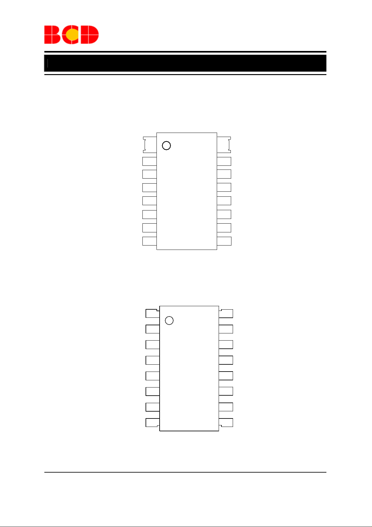
Pin Configuration
GH Package
(HTSSOP-14)
PGND
OUT2
VCC
VMIN
PWM
CF
FG
RD
1
2
3
4
5
6
7
GS Package
(SSOP-16)
OUT2
NC
VCC
VMIN
PWM
CF
FG
RD
Figure 2. Pin Configuration of AM4962 (Top View)
1
2
3
4
5
6
7
8
Apr. 2011 Rev. 1. 2 BCD Semiconductor Manufacturing Limited
2
14
13
12
11
10
9
8
16
15
14
13
12
11
10
9
PGND
OUT1
GND
CT
RADJ
HIN-
HB
HIN+
PGND
OUT1
GND
CT
RADJ
HIN-
HB
HIN+
Page 3

Data Sheet
SINGLE PHASE FULL WAVE DIRECT PWM MOTOR DRIVER AM4962
Pin Description
Pin Number
HTSSOP-14 SSOP-16
Pin Name Function
1 1
2
2 3
3 4
4 5
5 6
6 7
7 8
8 9
9 10
10 11
11 12
12 13
13 14
OUT2 Driver output 2
NC No connection
VCC Power supply
VMIN Minimum duty setting
PWM PWM pulse Input
CF PWM filter capacitor
FG Rotation speed indicator
RD Rotation/lock state indicator
HIN+ Hall sensor input +
HB Hall sensor bias regulator
HIN- Hall sensor input -
RADJ Slope K adjustable terminal
CT Lock and rotation setting capacitor terminal
GND Ground for control circuit
14 15
16
OUT1 Driver output 1
PGND Power ground
Apr. 2011 Rev. 1. 2 BCD Semiconductor Manufacturing Limited
3
Page 4
Data Sheet
SINGLE PHASE FULL WAVE DIRECT PWM MOTOR DRIVER AM4962
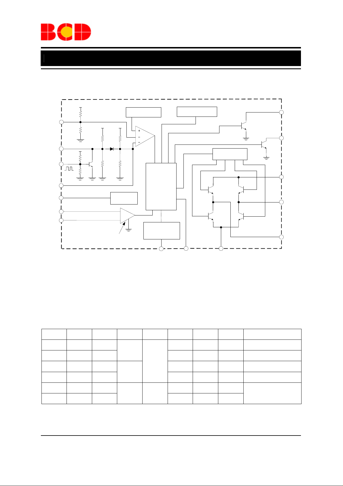
Functional Block Diagram
VMIN
RADJ
PWM
CF
HB
HIN+
HIN-
V+
3 (4)
11 (12)
V+
4 (5)
5 (6)
9 (10)
8 (9)
10 (11)
104k
42k
90k
54k
V+
V+
51k
56k
Hall
Bias
Hysteresis Amp
Triangle Wave
93k
18k
Control
Circuit
Lock Shutdown
and
Auto Restart
12 (13) 13 (14)
CT
Thermal
Shutdown
Pre-
driver
(16)
GND PGND
6 (7)
7 (8)
2 (3)
1 (1)
14 (15)
A (B)
A HTSSOP-14
B SSOP-16
Figure 3. Functional Block Diagram of AM4962
Truth Table (Note 1)
Items IN- IN+ CF CT OUT1 OUT2 FG Mode
FG
RD
VCC
OUT2
OUT1
1 H L H L L Rotation
L
2 L H
L H Off PWM off
L
3 H L Off L L
H
4 L H
L Off Off PWM off
Rotation Recirculate
5 H L H Off L
6 L H
L H
Off H Off
Lock Protection
Note 1: VCF(H)=5V, VCF(L) =1V, VCT(H)=5V, VCT(L) =0
Apr. 2011 Rev. 1. 2 BCD Semiconductor Manufacturing Limited
4
Page 5
Data Sheet
SINGLE PHASE FULL WAVE DIRECT PWM MOTOR DRIVER AM4962
Ordering Information
AM4962 -
Circuit Type G1: Green
Package
HTSSOP-14
SSOP-16
Package
GH: HTSSOP-14
GS: SSOP-16
Temperature
Range
-30 to 90°C
Part Number Marking ID
AM4962GH-G1 AM4962GH-G1
AM4962GHTR-G1 AM4962GH-G1
AM4962GS-G1 AM4962GS-G1
AM4962GSTR-G1 AM4962GS-G1
Blank: Tube
TR: Tape & Reel
Packing
Type
Tube
Tape & Reel
Tube
Tape & Reel
BCD Semiconductor's Pb-free products, as designated with "G1" suffix in the part number, are RoHS compliant
and green.
Apr. 2011 Rev. 1. 2 BCD Semiconductor Manufacturing Limited
5
Page 6

Data Sheet
SINGLE PHASE FULL WAVE DIRECT PWM MOTOR DRIVER AM4962
Absolute Maximum Ratings (Note 2)
Parameter Symbol Value Unit
Supply Voltage VCC 18 V
Output Current I
Output Voltage V
HB Output Current IHB 10 mA
RD Output Voltage VRD 18 V
FG Output Voltage VFG 18 V
RD Output Current IRD 10 mA
FG Output Current IFG 10 mA
Power Dissipation PD
Storage Temperature Range T
Thermal Resistance
(Junction to Ambient)
ESD (Human Body Model) ESD 2000 V
ESD (Machine Model) ESD 250 V
1.0 A
OUT
18 V
OUT
SSOP-16 0.8 W
HTSSOP-14 1.1 W
-55 to 150 °C
STG
θ
JA
SSOP-16 156
HTSSOP-14 114
°C/W
Note 2: Stresses greater than those listed under “Absolute Maximum Ratings” may cause permanent damage to
the device. These are stress ratings only, and functional operation of the device at these or any other conditions
beyond those indicated under “Recommended Operating Conditions” is not implied. Exposure to “Absolute
Maximum Ratings” for extended periods may affect device reliability.
Recommended Operating Conditions
Parameter Symbol Min Typ Max Unit
Supply Voltage VCC 3.5 12 16 V
Hall Input Voltage + (Note 3) V
Hall Input Voltage - (Note 3) V
PWM High Level Voltage V
Ambient Temperature TA -30
0.2
IN+
0.2
IN-
PWM
3 V
3 V
VCC-1 V
90 °C
Note 3: Hall input voltage range includes the am pl it ude of s i gnal .
Apr. 2011 Rev. 1. 2 BCD Semiconductor Manufacturing Limited
6
Page 7

Data Sheet
SINGLE PHASE FULL WAVE DIRECT PWM MOTOR DRIVER AM4962
Electrical Characteristics
(VCC=12V, TA=25°C, unless otherwise specified.)
Parameter Symbol Conditions Min Typ Max Unit
IQ1 VCT=0 10.18 15 18.76
Quiescent Current
I
VCT=5V 5.38 8 10.55
Q2
mA
Output Saturation Voltage at High
Side
Output Saturation Voltage at Low
Side
CPWM Frequency f
CF High Level Voltage V
CF Low Level Voltage V
VMIN Voltage V
RADJ Pin Voltage V
Hall Input Hysteresis V
I
V
SATH
I
V
SATL
18 25 32 kHz
OSC
V
CFH
V
CFL
3.4 3.7 4.0 V
MIN
ADJ
HYS
V
±10 ±20 mV
=200mA 1.0 1.17 V
SOURCE
=200mA 0.2 0.3 V
SINK
=0 3.2 3.6 3.75 V
PWM
=5 1.83 1.95 2.15 V
PWM
PWM
=0
3.6 3.8 4.4 V
Hall Bias Voltage VHB IHB=5mA 1.1 1.25 1.4 V
CT High Level Voltage V
CT Low Level Voltage V
CT Charge Current I
CT Discharge Current I
3.55 3.7 3.88 V
CTH
1.55 1.7 1.85 V
CTL
1.5 2 2.85 µA
CHG
0.14 0.2 0.285 µA
DHG
CT Charge and Discharge Ratio RCD I
FG Output Low Level Voltage V
FG Leakage Current I
RD Output Low Level Voltage V
RD Leakage Current I
FGL
LFG
RDL
LRD
CHG/IDHG
IFG=5mA 0.2 0.3 V
VFG=12V 30 µA
IRD=5mA 0.2 0.3 V
VRD=12V 30 µA
8.5 10 14.5
Apr. 2011 Rev. 1. 2 BCD Semiconductor Manufacturing Limited
7
Page 8

Data Sheet
SINGLE PHASE FULL WAVE DIRECT PWM MOTOR DRIVER AM4962
Typical Performance Characteristics
20
20
16
16
12
12
8
Quiescent Current (mA)
4
0
-50 -25 0 25 50 75 100 125
Ambient Temperature (OC)
VCC=12V
IQ1(VCT=L)
IQ2(VCT=H)
8
Quiescent Current (mA)
4
0
4 6 8 1012141618
Supply Voltage (V)
TA=25oC
IQ1(VCT=L)
IQ2(VCT=H)
Figure 4. Quiescent Current vs. Ambient Temperature Figure 5. Quiescent Current vs. Supply Voltage
2.0
1.6
1.2
V
V
V
V
SATH1
SATH2
SATL1
SATL2
VCC=12V, TA=25oC
0.8
Output Saturation Voltage (V)
0.4
0.0
0 100 200 300 400 500 600 700 800 900 1000
Output Current (mA)
Figure 6. Output Saturation Voltage vs. Figure 7. Power Dissipation vs.
Output Current Ambient Temperature
1.2
1.0
0.8
0.6
0.4
Allowable Power Dissipation (W)
0.2
0.0
-20 0 20 40 60 80 100
Ambient Temperature (OC)
Package: HTSSOP-14
90
Apr. 2011 Rev. 1. 2 BCD Semiconductor Manufacturing Limited
8
Page 9

Data Sheet
SINGLE PHASE FULL WAVE DIRECT PWM MOTOR DRIVER AM4962
Typical Performance Characteristics (Continued)
1.2
1.0
0.8
0.6
0.4
0.2
Allowed Power Dissipation (W)
0.0
-20 0 20 40 60 80 100 120
Ambient Temperature (OC)
Figure 8. Power Dissipation vs. Ambient Temperature
Package: SSOP-16
90
Apr. 2011 Rev. 1. 2 BCD Semiconductor Manufacturing Limited
9
Page 10

Data Sheet
SINGLE PHASE FULL WAVE DIRECT PWM MOTOR DRIVER AM4962
Operating Diagram
Figure 9. Operating Diagram of AM4962
Apr. 2011 Rev. 1. 2 BCD Semiconductor Manufacturing Limited
10
Page 11

Data Sheet
SINGLE PHASE FULL WAVE DIRECT PWM MOTOR DRIVER AM4962
Typical Application (Note 4)
1 (1)
D1
1μF
V+
C1
C3
1μF
2 (3)
3 (4)
4 (5)
5 (6)
6 (7)
7 (8)
VCC
L1
AM4962
OUT2 OUT1
VCC GND
VMIN CT
PWM RADJ
CF HIN-
FG HB
RD HIN+
PGND
14 (15)
13 (14)
12 (13)
11 (12)
10 (11)
9 (10)
8 (9)
Hall
100
80
60
C2
0.47μF
40
Output Duty Cycle (%)
20
Min. Duty Cycle
0
0 102030405060708090100
Input PWM Duty Cycle (%)
Figure 10
Application 1 (Default)
VCC
D1
V+
D2
1 (1)
C1
F
1
R1
R2
C3
F
1
R3
R4
2 (3)
3 (4)
4 (5)
5 (6)
6 (7)
7 (8)
L1
AM4962
OUT2 OUT1
VCC GND
VMIN CT
PWM RADJ
CF HIN-
FG HB
RD HIN+
PGND
14 (15)
13 (14)
12 (13)
11 (12)
10 (11)
9 (10)
8 (9)
Hall
Slope K
D3
Max. Duty Cycle
C2
F
0.47
V+
R5
R6
Application 2 (Slope K and Minimum/Maximum Duty Adjustable)
Note: D2 and D3 are recommended to be used when the current in coil L1 is higher than 300mA.
Figure 11. Typical Applications of AM4962
Apr. 2011 Rev. 1. 2 BCD Semiconductor Manufacturing Limited
11
Page 12

Data Sheet
SINGLE PHASE FULL WAVE DIRECT PWM MOTOR DRIVER AM4962
Typical Application (Note 4, Continued)
Note 4 (Refer to application circuit 2 unless otherwise noted.):
Adjust slope K of output PWM's duty vs. input PWM's duty
1. The default K is about 0.8 (application circuit 1).
2. Adding R5 can increase K (see Figure 12).
3. Adding R6 can decrease K (see Figure 13).
100
80
60
R5=270k, R1, R2, R3, R4, R6 Open
R5=560k, R1, R2, R3, R4, R6 Open
R1, R2, R3, R4, R5, R6 Open
40
Output Duty Cycle (%)
20
0
0 102030405060708090100
Input PWM Duty Cycle (%)
Figure 12 Figure 13
Adjust minimum duty of output PWM:
1. The default minimum duty of output PWM is about 20% (application circuit 1, Figure 10).
2. Decreasing R2 can increase minimum output PWM duty (see Figure 14).
3. Adding R5 can decrease minimum output PWM duty (see Figure 15).
80
70
60
50
R1=15k,R3,R4,R5,R6 open
100
80
60
40
Output Duty Cycle (%)
20
0
0 102030405060708090100
R6=100k, R1, R2, R3, R4, R5 Open
R6=270k, R1, R2, R3, R4, R5 Open
R1, R2, R3, R4, R5, R6 Open
Input PWM Duty Cycle (%)
100
80
60
R1, R2, R3, R4, R6 open
40
30
Minimum Duty Cycle (%)
20
10
3.5k
4.0k
R2 (Ω)
5.5k
5.0k4.5k
6.0k
6.5k
40
Minimum Duty Cycle (%)
20
0
390K 560K 820K 1M 2.2M 4.7M 8.2M
R5 (Ω)
Figure 14 Figure 15
Apr. 2011 Rev. 1. 2 BCD Semiconductor Manufacturing Limited
12
Page 13

Data Sheet
SINGLE PHASE FULL WAVE DIRECT PWM MOTOR DRIVER AM4962
Typical Application (Note 4, Continued)
Adjust maximum duty of output PWM:
1. The default maximum output PWM duty is 100% (application circuit 1).
2. Adding R3 can decrease maximum output PWM duty (see Figure 16).
3. Adding R4 can increase maximum output PWM duty (see Figure 17).
100
80
60
R3=390k, R1, R2, R4, R5, R6 Open
R3=1M, R1, R2, R4, R5, R6 Open
R1, R2, R3, R4, R5, R6 Open
40
Output Duty Cycle (%)
20
0
0 102030405060708090100
PWM (%)
Figure 16 Figure 17
100
Output Duty Cycle (%)
80
60
40
20
0
0 102030405060708090100
R4=150k, R1, R2, R3, R4, R6 Open
R4=390k, R1, R2, R3, R5, R6 Open
R1, R2, R3, R4, R5, R6 Open
PWM (%)
Apr. 2011 Rev. 1. 2 BCD Semiconductor Manufacturing Limited
13
Page 14

Data Sheet
SINGLE PHASE FULL WAVE DIRECT PWM MOTOR DRIVER AM4962
Mechanical Dimensions
HTSSOP-14 Unit: mm(inch)
6.350(0.250)
6.550(0.258)
0.750(0.030)
0.850(0.033)
1.300(0.051)
BSC
1.470(0.058)
1.570(0.062)
1.450(0.057)
1.550(0.061)
0.650(0.026)
BSC
1.200(0.047)
0.340(0.013)
0.540(0.021)
6.200(0.244)
6.600(0.260)
MAX
0.050(0.002)
0.200(0.008)
0.900(0.035)
1.050(0.041)
4. 300(0. 169)
4. 500(0. 177)
R0.090(0.004)
R0.090(0.004)
0.250(0.010)
0.450(0.018)
0.750(0.030)
MIN
BSC
0.200(0.008)
MIN
MIN
SEE
DETAIL A
0.200(0.008) or 1.480(0.058)
0.280(0.011) or 1.610(0.063)
0.100(0.004)
0.190(0.007)
10
14
1.000(0.039)
REF
DETAIL A
BASE METAL
0.100(0.004)
0.150(0.006)
0.200(0.008) or 1.470(0.058)
0.240(0.009) or 1.570(0.062)
0
8
Note: Eject hole, oriented hole and mold mark is optional.
Apr. 2011 Rev. 1. 2 BCD Semiconductor Manufacturing Limited
14
Page 15

Data Sheet
SINGLE PHASE FULL WAVE DIRECT PWM MOTOR DRIVER AM4962
Mechanical Dimensions (Continued)
SSOP-16 Unit: mm(inch)
o
o
Φ
o
o
o
o
Apr. 2011 Rev. 1. 2 BCD Semiconductor Manufacturing Limited
15
Page 16

BCD Semiconductor Manufacturing Limited
IMPORTANT NOTICE
IMPORTANT NOTICE
BCD Semiconductor Manufacturing Limited reserves the right to make changes without further notice to any products or specifi-
BCD Semiconductor Manufacturing Limited reserves the right to make changes without further notice to any products or specifi-
cations herein. BCD Semiconductor Manufacturing Limited does not assume any responsibility for use of any its products for any
cations herein. BCD Semiconductor Manufacturing Limited does not assume any responsibility for use of any its products for any
particular purpose, nor does BCD Semiconductor Manufacturing Limited assume any liability arising out of the application or use
particular purpose, nor does BCD Semiconductor Manufacturing Limited assume any liability arising out of the application or use
of any its products or circuits. BCD Semiconductor Manufacturing Limited does not convey any license under its patent rights or
of any its products or circuits. BCD Semiconductor Manufacturing Limited does not convey any license under its patent rights or
other rights nor the rights of others.
other rights nor the rights of others.
http://www.bcdsemi.com
MAIN SITE
MAIN SITE
- Headquarters
BCD Semiconductor Manufacturing Limited
BCD Semiconductor Manufactur ing Limited
- Wafer Fab
No. 1600, Zi Xing Road, Shanghai ZiZhu Science-based Industrial Park, 200241, China
Shanghai SIM-BCD Semiconductor Manufacturing Limited
Tel: +86-21-24162266, Fax: +86-21-24162277
800, Yi Shan Road, Shanghai 200233, China
Tel: +86-21-6485 1491, Fax: +86-21-5450 0008
REGIONAL SALES OFFICE
Shenzhen Office
REGIONAL SALES OFFICE
Shanghai SIM-BCD Semiconductor Manufacturing Co., Ltd., Shenzhen Office
Shenzhen Office
Unit A Room 1203, Skyworth Bldg., Gaoxin Ave.1.S., Nanshan District, Shenzhen,
Shanghai SIM-BCD Semiconductor Manufacturing Co., Ltd. Shenzhen Office
China
Advanced Analog Circuits (Shanghai) Corporation Shenzhen Office
Tel: +86-755-8826 7951
Room E, 5F, Noble Center, No.1006, 3rd Fuzhong Road, Futian District, Shenzhen 518026, China
Fax: +86-755-8826 7865
Tel: +86-755-8826 7951
Fax: +86-755-8826 7865
- Wafer Fab
BCD Semiconductor Manufacturing Limited
Shanghai SIM-BCD Semiconductor Manufacturing Co., Ltd.
- IC Design Group
800 Yi Shan Road, Shanghai 200233, China
Advanced Analog Circuits (Shanghai) Corporation
Tel: +86-21-6485 1491, Fax: +86-21-5450 0008
8F, Zone B, 900, Yi Shan Road, Shanghai 200233, China
Tel: +86-21-6495 9539, Fax: +86-21-6485 9673
Taiwan Office
BCD Semiconductor (Taiwan) Company Limited
Taiwan Office
4F, 298-1, Rui Guang Road, Nei-Hu District, Taipei,
BCD Semiconductor (Taiwan) Company Limited
Tai wan
4F, 298-1, Rui Guang Road, Nei-Hu District, Taipei,
Tel: +886-2-2656 2808
Taiwan
Fax: +886-2-2656 2806
Tel: +886-2-2656 2808
Fax: +886-2-2656 2806
USA Office
BCD Semiconductor Corp.
USA Office
30920 Huntwood Ave. Hayward,
BCD Semiconductor Corporation
CA 94544, USA
30920 Huntwood Ave. Hayward,
Tel : +1-510-324-2988
CA 94544, U.S.A
Fax: +1-510-324-2788
Tel : +1-510-324-2988
Fax: +1-510-324-2788
 Loading...