

Page 1
Data Sheet
SINGLE PHASE FULL WAVE DIRECT PWM MOTOR DRIVER AM4961
General Description
The AM4961 is a full wave driver IC with PWM control function. It is used for single phase motor and is
capable of speed control by changing output duty
cycle.
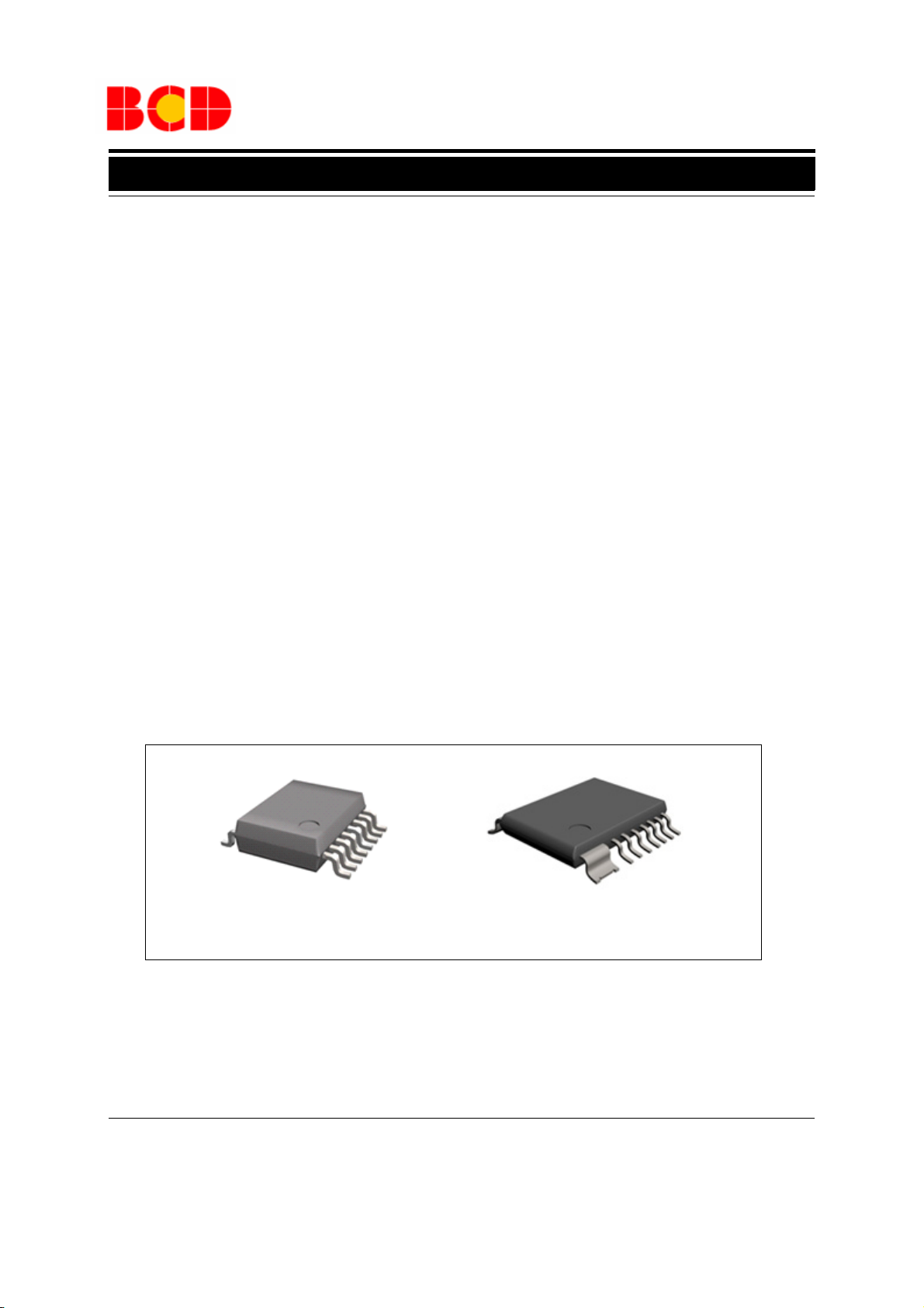
The AM4961 is available in SSOP-16 and HTSSOP14 packages.
Features
· Built-in Hall Bias Circuit
· Built-in PWM Speed Control Circuit
· Built-in Minimal Speed Setup Circuit
· Rotation Speed Indication (FG)
· Rotation or Lock State Indication (RD)
· Built-in Thermal Shutdown Circuit
· Lock Protection
· Output Current Limit
Application
· CPU Cooler Fan in PC
· Brushless DC Motor Driver
SSOP-16
Figure 1. Package Types of AM4961
May. 2011 Rev. 2. 4 BCD Semiconductor Manufacturing Limited
1
HTSSOP-14
Page 2
Data Sheet
SINGLE PHASE FULL WAVE DIRECT PWM MOTOR DRIVER AM4961
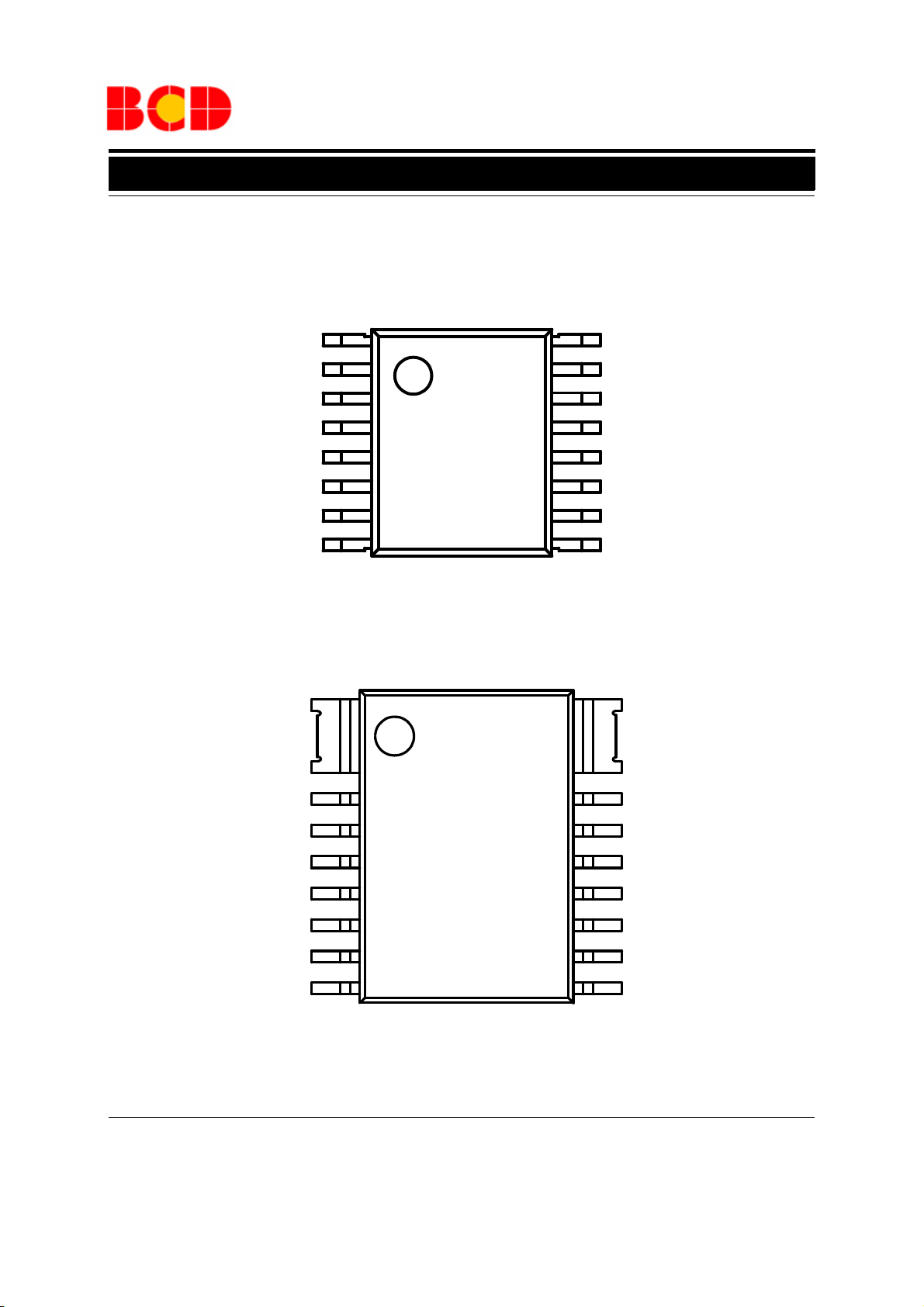
Pin Configuration
GS Package
(SSOP-16)
OUT2
NC
VCC
VMIN
VPWM
COSC
FG
RD
PGND
1
2
3
4
5
6
7
8
GH Package
(HTSSOP-14)
16
15
14
13
12
11
10
PGND
OUT1
GND
CT
VREF
HIN-
HB
9
HIN+
PGND
OUT2
VCC
VMIN
VPWM
COSC
FG
RD
Figure 2. Pin Configuration of AM4961 (Top View)
May. 2011 Rev. 2. 4 BCD Semiconductor Manufacturing Limited
1
2
3
4
5
6
7
14
13
12
11
10
9
8
OUT1
GND
CT
VREF
HIN-
HB
HIN+
2
Page 3

Data Sheet
SINGLE PHASE FULL WAVE DIRECT PWM MOTOR DRIVER AM4961
Pin Description
Pin Number
HTSSOP-14 SSOP-16
1 1 OUT2 Driver output 2
2 NC No connection
2 3 VCC Power supply
3 4 VMIN Minimum duty setting
4 5 VPWM Adjustable Input
5 6 COSC Oscillator capacitor
6 7 FG Rotation speed indicator
7 8 RD Rotation/lock state indicator
8 9 HIN+ Hall sensor input +
9 10 HB Hall sensor bias regulator
10 11 HIN- Hall sensor input -
11 12 VREF Reference voltage regulator
12 13 CT Lock and rotation setting capacitor terminal
13 14 GND Ground for control circuit
14 15 OUT1 Driver output 1
16 PGND Power ground
Pin Name Function
May. 2011 Rev. 2. 4 BCD Semiconductor Manufacturing Limited
3
Page 4
Data Sheet
Lock Shutdown
and
Auto Restart
Voltage
Reference
Hall Bias
Thermal Shutdown
Hysteresis Amp
Control
Circuit
Oscillation Circuit
CT
VCC
VREF
HB
HIN+
HIN-
VMIN
VPWM
COSC
GND
PGND
OUT1
OUT2
RD
FG
2 (3)
11 (12)
9 (10)
8 (9)
10 (11)
3 (4)
4 (5)
5 (6)
13 (14)
(16)
14 (15)
1 (1)
7 (8)
6 (7)
12 (13)
Pre-driver
SINGLE PHASE FULL WAVE DIRECT PWM MOTOR DRIVER AM4961
Functional Block Diagram
A (B)
May. 2011 Rev. 2. 4 BCD Semiconductor Manufacturing Limited
A for 14-pin
B for 16-pin
Figure 3. Functional Block Diagram of AM4961
4
Page 5
Data Sheet
SINGLE PHASE FULL WAVE DIRECT PWM MOTOR DRIVER AM4961
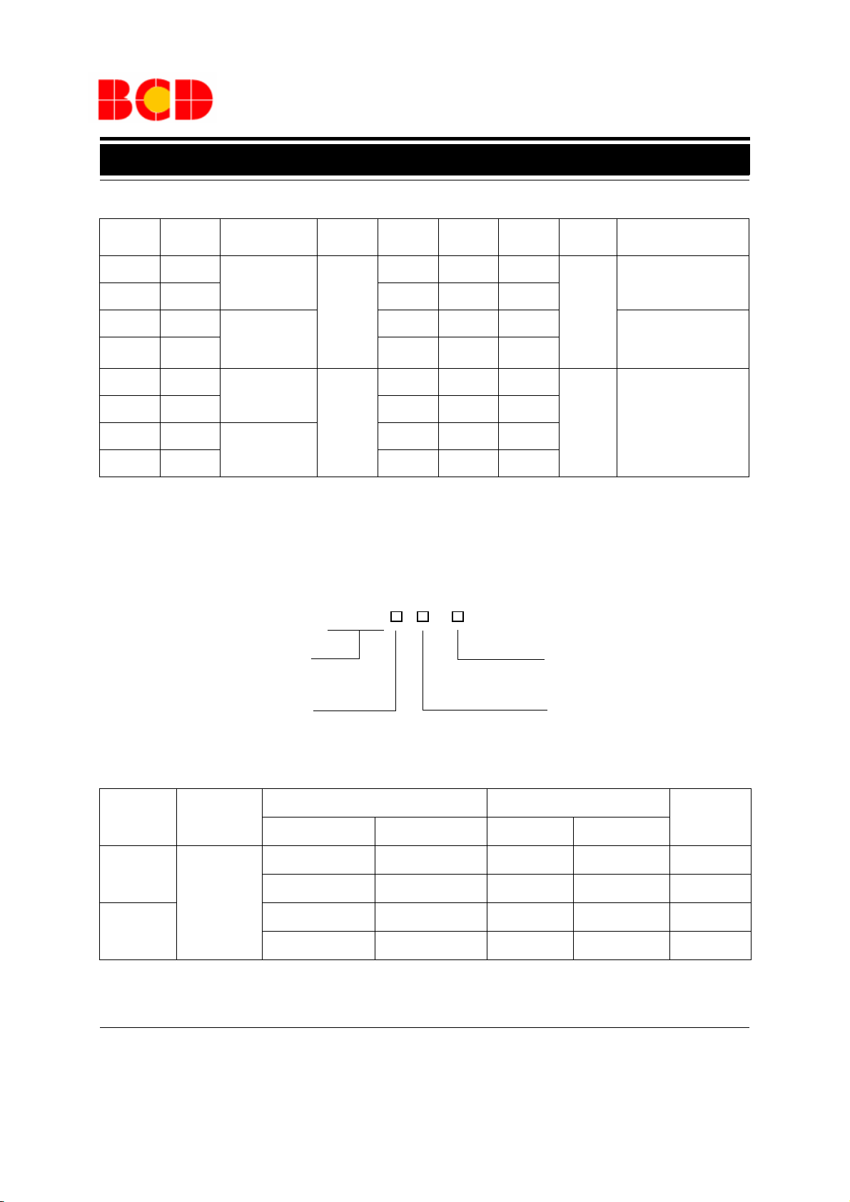
Truth Table
HIN- HIN+ COSC (Note 1) CT OUT1 OUT2 FG RD Mode
HL
, V
H
L
H
L
OSC
(L) <V
PWM
L
H
.
LH LHOFF
HL
LH LOFFOFF
HL
L H OFF H OFF
HL
L H OFF OFF OFF
Note 1: V
OSC
(H) >V
PWM
HLL
OFF L L
HOFFL
OFF OFF L
Ordering Information
AM4961 -
Circuit Type
Rotation (Drive)
L
Rotation (Recirculate)
OFF Lock Protection
E1: Lead Free
G1: Green
Package
GS: SSOP-16
TR: Tape and Reel
Blank: Tube
GH: HTSSOP-14
Package
SSOP-16
HTSSOP-14
BCD Semiconductor's Pb-free products, as designated with "E1" suffix in the part number, are RoHS compliant. Products with
"G1" suffix are available in green packages.
May. 2011 Rev. 2. 4 BCD Semiconductor Manufacturing Limited
Te mp er a tu re
Range
-30 to 90
o
C
Lead Free Green Lead Free Green
AM4961GS-E1 AM4961GS-G1 AM4961GS AM4961GS-G1 Tube
AM4961GSTR-E1 AM4961GSTR-G1 AM4961GS AM4961GS-G1 Tape & Reel
AM4961GH-E1 AM4961GH-G1 AM4961GH AM4961GH-G1 Tube
AM4961GHTR-E1 AM4961GHTR-G1 AM4961GH AM4961GH-G1 Tape & Reel
Part Number Marking ID
Packing
Typ e
5
Page 6

Data Sheet
SINGLE PHASE FULL WAVE DIRECT PWM MOTOR DRIVER AM4961
Absolute Maximum Ratings (Note 2)
Parameter Symbol Value Unit
Supply Voltage V
Output Current I
Output Voltage V
HB Output Current I
VPWM Input Voltage V
RD Output Voltage V
FG Output Voltage V
RD Output Current I
FG Output Current I
CC
OUT
OUT
HB
PWM
RD
FG
RD
FG
18 V
1.0 A
18 V
10 mA
6V
18 V
18 V
10 mA
10 mA
SSOP-16 0.8 W
Power Dissipation (Note 3) P
Storage Temperature Range T
D
STG
HTSSOP-14 1.1 W
-55 to 150
o
C
ESD (Human Body Model) ESD 2000 V
ESD (Machine Model) ESD 250 V
Note 2: Stresses greater than those listed under "Absolute Maximum Ratings" may cause permanent damage to the device.
These are stress ratings only, and functional operation of the device at these or any other conditions beyond those indicated
under "Recommended Operating Conditions" is not implied. Exposure to "Absolute Maximum Ratings" for extended periods
may affect device reliability.
Note 3: T
=25oC, no external heatsink.
A
Recommended Operating Conditions
Parameter Symbol Min Typ Max Unit
Supply Voltage V
Hall Input Voltage + (Note 4) V
Hall Input Voltage - (Note 4) V
Ambient Temperature T
CC
IN+
IN-
A
Note 4: Hall input voltage range includes the amplitude of signal.
May. 2011 Rev. 2. 4 BCD Semiconductor Manufacturing Limited
6
3.5 12 16 V
0.2 3 V
0.2 3 V
-30 90
o
C
Page 7

Data Sheet
SINGLE PHASE FULL WAVE DIRECT PWM MOTOR DRIVER AM4961
Electrical Characteristics
(VCC=12V, TA=25oC, unless otherwise specified.)
Parameter Symbol Conditions Min Typ Max Unit
Quiescent Current
VREF Voltage
Output Saturation Voltage at
High Side
Output Saturation Voltage at
Low Side
COSC Frequency
COSC High Level Voltage
COSC Low Level Voltage
Hall Input Hysteresis
Hall Bias Voltage
CT High Level Voltage
CT Low Level Voltage
CT Charge Current
CT Discharge Current
I
I
V
V
V
f
V
V
V
V
V
V
I
I
Q1
Q2
REF
SATH
SATL
OSC
OSCH
OSCL
HYS
HB
CTH
CTL
CHG
DHG
Lock Off 10.2 15 18.76
Lock On 5.38 8 10.55
I
=5mA
REF
I
SOURCE
I
SINK
C
OSC
=200mA
=200mA
=100pF
5.8 6 6.2 V
1.0 1.17 V
0.2 0.3 V
18 25 32 kHz
3.45 3.6 3.75 V
1.83 1.95 2.07 V
±10 ±20 mV
IHB=5mA
1.1 1.25 1.4 V
3.55 3.7 3.88 V
1.55 1.7 1.85 V
1.5 2 2.85 μA
0.14 0.2 0.285 μA
mA
CT Charge and Discharge Ratio
FG Output Low Level Voltage
FG Leakage Current
RD Output Low Level Voltage
RD Leakage Current
May. 2011 Rev. 2. 4 BCD Semiconductor Manufacturing Limited
R
V
I
V
I
CD
FGL
LFG
RDL
LRD
I
CHG/IDHG
IFG=5mA
VFG=12V
IRD=5mA
VRD=12V
8.5 10 14.5
0.2 0.3 V
30 μA
0.2 0.3 V
30 μA
7
Page 8

Data Sheet
-50 0 50 100 150 200
0
4
8
12
16
20
VCC=12V
Rotation Mode
I
Q1
(mA)
TA (OC)
44688101212 14 1616 18
0
4
8
12
16
20
I
Q1
(mA)
V
CC
(V)
TA=25OC
Rotation Mode
0 200 400 600 800 1000
0.0
0.5
1.0
1.5
2.0
V
SATH
(V)
I
OUT
(mA)
VCC=12V
0 200 400 600 800 1000
0.0
0.5
1.0
1.5
2.0
V
SATL
(V)
I
OUT
(mA)
VCC=12V
SINGLE PHASE FULL WAVE DIRECT PWM MOTOR DRIVER AM4961
Typical Performance Characteristics
Figure 4.Quiescent Current vs. Ambient Temperature
Figure 6.
Output Saturation Voltage (High)
vs. Output Current
Figure 5. Quiescent Current vs. Supply Voltage
Figure 7. Output Saturation Voltage (Low)
vs. Output Current
May. 2011 Rev. 2. 4 BCD Semiconductor Manufacturing Limited
8
Page 9

Data Sheet
-20 0 20 40 60 80 100
0.0
0.2
0.4
0.6
0.8
1.0
1.2
P
D
(W)
TA (OC)
90
Package: HTSSOP-14
No External Heatsink
-20 0 20 40 60 80 100 120
0.0
0.2
0.4
0.6
0.8
1.0
1.2
P
D
(W)
TA (OC)
90
Package: SSOP-16
No External Heatsink
SINGLE PHASE FULL WAVE DIRECT PWM MOTOR DRIVER AM4961
Typical Performance Characteristics (Continued)
Figure 8. Power Dissipation vs. Ambient Temperature
Figure 9. Power Dissipation vs. Ambient Temperature
May. 2011 Rev. 2. 4 BCD Semiconductor Manufacturing Limited
9
Page 10

Data Sheet
M
Lowest speed setting voltage
VPWM adjustable Voltage
f
OSC
=25kHz (C
OSC
=100pF)
VMIN Voltage
COSC Output
Low Speed
PWM Variable
High Speed
V
CC
0V
FG Output
V
osc
V
osc
SINGLE PHASE FULL WAVE DIRECT PWM MOTOR DRIVER AM4961
Operating Diagram
Note 5:
1. Low Speed Setting Mode
When VPWM voltage is higher than VMIN pin voltage,
motor speed is settable by VMIN pin voltage. The minimum drive duty cycle is settable by comparing COSC
oscillating voltage and VMIN pin voltage.
VPWM voltage is decided by variation of PWM duty.
2. Variable Speed Setting Mode
When VPWM voltage is lower than VMIN pin voltage,
PWM control system works by comparing VPWM voltage
and COSC voltage. If VPWM voltage is higher, the ON
duty cycle of the upper side transistors will be minimized
and motor speed becomes lower. Vice versa.
3. Full Speed Rotation Mode
May. 2011 Rev. 2. 4 BCD Semiconductor Manufacturing Limited
Figure 10. Operating Diagram of AM4961 (Note 5)
At a certain PWN duty, when VPWM voltage is lower than
the low side of COSC output voltage, the motor will run at
full speed.
10
Page 11

Data Sheet
OUT2 OUT1
VCC GND
VMIN CT
VPWM VREF
COSC HIN-
FG HB
RD HIN+
Hall
AM4961
D1
C1
1μF or greater
R1
27k
R2
10k
R4
39k
R6 330k
R7
100k
R5
100k
PWM
VCC
L1
R3
7.5k
R8 68k
C2
0.33μF
C3
100pF
C4
0.47μF
1 (1)
2 (3)
3 (4)
4 (5)
5 (6)
6 (7)
7 (8) 8 (9)
9 (10)
10 (11)
11 (12)
12 (13)
13 (14)
14 (15)
PGND
(16)
SINGLE PHASE FULL WAVE DIRECT PWM MOTOR DRIVER AM4961
Typical Application
Figure 11. Typical Application of AM4961 (Note 6)
Note 6:
*1. Ground Line Layout
PGND is connected to motor supply stage and GND is
connected to control stage. All ground lines from control
When C
*5. FG Output
FG output terminal is open collector output which varies
with phase change.
is 100pF, the COSC frequency will be 25kHz.
CP
stage are connected to GND.
*6. RD Output
*2. Stability of Power Supply
RD output terminal is open collector output. It is low at
C1 is employed to stabilize V
. Its capacitance is no less
CC
rotation mode and high when stopped.
than 1μF.
*3. Hall Input
*7. HB Pin
This pin is available to output a 1.25V Hall bias voltage.
To avoid noise, the shortest line is recommended to connect with Hall stage which has about 20mV hysteresis.
Thus, the ideal Hall input is 50mV or over.
*4. COSC Capacitor
May. 2011 Rev. 2. 4 BCD Semiconductor Manufacturing Limited
*8. VMIN Pin
If this pin is disused, connect it directly with VPWM, the
minimum duty cycle will be 10%.
11
Page 12

Data Sheet
3.800(0.150)
4.000(0.157)
0.200(0.008)
0.300(0.012)
0.800(0.031)
0.635(0.025)
BSC
0.900(0.035)1.000(0.039)
0.100(0.004)
0.250(0.010)
1.350(0.053)
1.750(0.069)
0.400(0.016)
1.270(0.050)
4.700(0.185)
5.100(0.201)
5.800(0.228)
6.200(0.244)
0.650(0.026)
0.750(0.030)
0.200(0.008)
0.250(0.010)
1.350(0.053)
1.550(0.061)
0.020(0.001)
0.050(0.002)
R0.150(0.006)
R0.150(0.006)
0.250(0.010)
SEE
DETAIL A
7
7
8
8
0.150(0.006)
0.250(0.010)
0
8
DETAIL A
Note: Eject hole, oriented hole and mold mark is optional.
SINGLE PHASE FULL WAVE DIRECT PWM MOTOR DRIVER AM4961
Mechanical Dimensions
SSOP-16 Unit: mm(inch)
°
°
Φ
°
°
°
°
May. 2011 Rev. 2. 4 BCD Semiconductor Manufacturing Limited
12
Page 13

Data Sheet
6.350(0.250)
6.550(0.258)
1.470(0.058)
1.570(0.062)
1. 450(0.05 7)
1. 550(0.06 1)
0.750(0.030)
0.850(0.033)
0. 650(0.02 6)
BSC
1.300(0.051)
BSC
6.200(0.244)
6.600(0.260)
0.340(0.013)
0.540(0.021)
1.200(0.047)
MAX
0.050(0.002)
0.200(0.008)
0.900(0.035)
1.050(0.041)
4.300(0.169)
4.500(0.177)
SEE
DETAIL A
0.250(0. 010)
BSC
R0.090(0.004)
MIN
R0.090(0.004)
MIN
0.200(0.008)
MIN
10
14
0.450(0.018)
0.750(0.030)
1.000(0. 039)
REF
0
8
DETAIL A
°
°
°
°
Note: Eject hole, oriented hole and mold mark is optional.
0.200(0.008) or 1.480(0.058)
0.280(0.011) or 1.610(0.063)
0.100(0.004)
0.150(0.006)
0.100(0.004)
0.190(0.007)
0.200(0.008) or 1.470(0.058)
0.240(0.009) or 1.570(0.062)
BASE METAL
ٛ
ٛ
Φ
Φ
SINGLE PHASE FULL WAVE DIRECT PWM MOTOR DRIVER AM4961
Mechanical Dimensions (Continued)
HTSSOP-14 Unit: mm(inch)
May. 2011 Rev. 2. 4 BCD Semiconductor Manufacturing Limited
13
Page 14

BCD Semiconductor Manufacturing Limited
IMPORTANT NOTICE
IMPORTANT NOTICE
BCD Semiconductor Manufacturing Limited reserves the right to make changes without further notice to any products or specifi-
BCD Semiconductor Manufacturing Limited reserves the right to make changes without further notice to any products or specifi-
cations herein. BCD Semiconductor Manufacturing Limited does not assume any responsibility for use of any its products for any
cations herein. BCD Semiconductor Manufacturing Limited does not assume any responsibility for use of any its products for any
particular purpose, nor does BCD Semiconductor Manufacturing Limited assume any liability arising out of the application or use
particular purpose, nor does BCD Semiconductor Manufacturing Limited assume any liability arising out of the application or use
of any its products or circuits. BCD Semiconductor Manufacturing Limited does not convey any license under its patent rights or
of any its products or circuits. BCD Semiconductor Manufacturing Limited does not convey any license under its patent rights or
other rights nor the rights of others.
other rights nor the rights of others.
http://www.bcdsemi.com
MAIN SITE
MAIN SITE
- Headquarters
BCD Semiconductor Manufacturing Limited
BCD Semiconductor Manufactur ing Limited
- Wafer Fab
No. 1600, Zi Xing Road, Shanghai ZiZhu Science-based Industrial Park, 200241, China
Shanghai SIM-BCD Semiconductor Manufacturing Limited
Tel: +86-21-24162266, Fax: +86-21-24162277
800, Yi Shan Road, Shanghai 200233, China
Tel: +86-21-6485 1491, Fax: +86-21-5450 0008
REGIONAL SALES OFFICE
Shenzhen Office
REGIONAL SALES OFFICE
Shanghai SIM-BCD Semiconductor Manufacturing Co., Ltd., Shenzhen Office
Shenzhen Office
Unit A Room 1203, Skyworth Bldg., Gaoxin Ave.1.S., Nanshan District, Shenzhen,
Shanghai SIM-BCD Semiconductor Manufacturing Co., Ltd. Shenzhen Office
China
Advanced Analog Circuits (Shanghai) Corporation Shenzhen Office
Tel: +86-755-8826 7951
Room E, 5F, Noble Center, No.1006, 3rd Fuzhong Road, Futian District, Shenzhen 518026, China
Fax: +86-755-8826 7865
Tel: +86-755-8826 7951
Fax: +86-755-8826 7865
- Wafer Fab
BCD Semiconductor Manufacturing Limited
Shanghai SIM-BCD Semiconductor Manufacturing Co., Ltd.
- IC Design Group
800 Yi Shan Road, Shanghai 200233, China
Advanced Analog Circuits (Shanghai) Corporation
Tel: +86-21-6485 1491, Fax: +86-21-5450 0008
8F, Zone B, 900, Yi Shan Road, Shanghai 200233, China
Tel: +86-21-6495 9539, Fax: +86-21-6485 9673
Taiwan Office
BCD Semiconductor (Taiwan) Company Limited
Taiwan Office
4F, 298-1, Rui Guang Road, Nei-Hu District, Taipei,
BCD Semiconductor (Taiwan) Company Limited
Tai wan
4F, 298-1, Rui Guang Road, Nei-Hu District, Taipei,
Tel: +886-2-2656 2808
Taiwan
Fax: +886-2-2656 2806
Tel: +886-2-2656 2808
Fax: +886-2-2656 2806
USA Office
BCD Semiconductor Corp.
USA Office
30920 Huntwood Ave. Hayward,
BCD Semiconductor Corporation
CA 94544, USA
30920 Huntwood Ave. Hayward,
Tel : +1-510-324-2988
CA 94544, U.S.A
Fax: +1-510-324-2788
Tel : +1-510-324-2988
Fax: +1-510-324-2788
 Loading...