Page 1

BTL Drive Single-phase Full-wave Fan Motor Driver AM4953
Data Sheet
General Description
The AM4953 is a single-phase BTL output fan motor
driver designed by bipolar process. This IC
features high efficiency, silent operation and includes
lock shutdown and automatic restart functions. When
the motor is under lock condition, the lock
shutdown function turns off the output current. When
the lock condition is removed, the IC will
restart automatically and allow DC fan to run. It is
applied for high reliability and low noise application,
such as personal computers, notebook, car audio,
CPU cooling systems and power supplies in
consumer electronics systems.
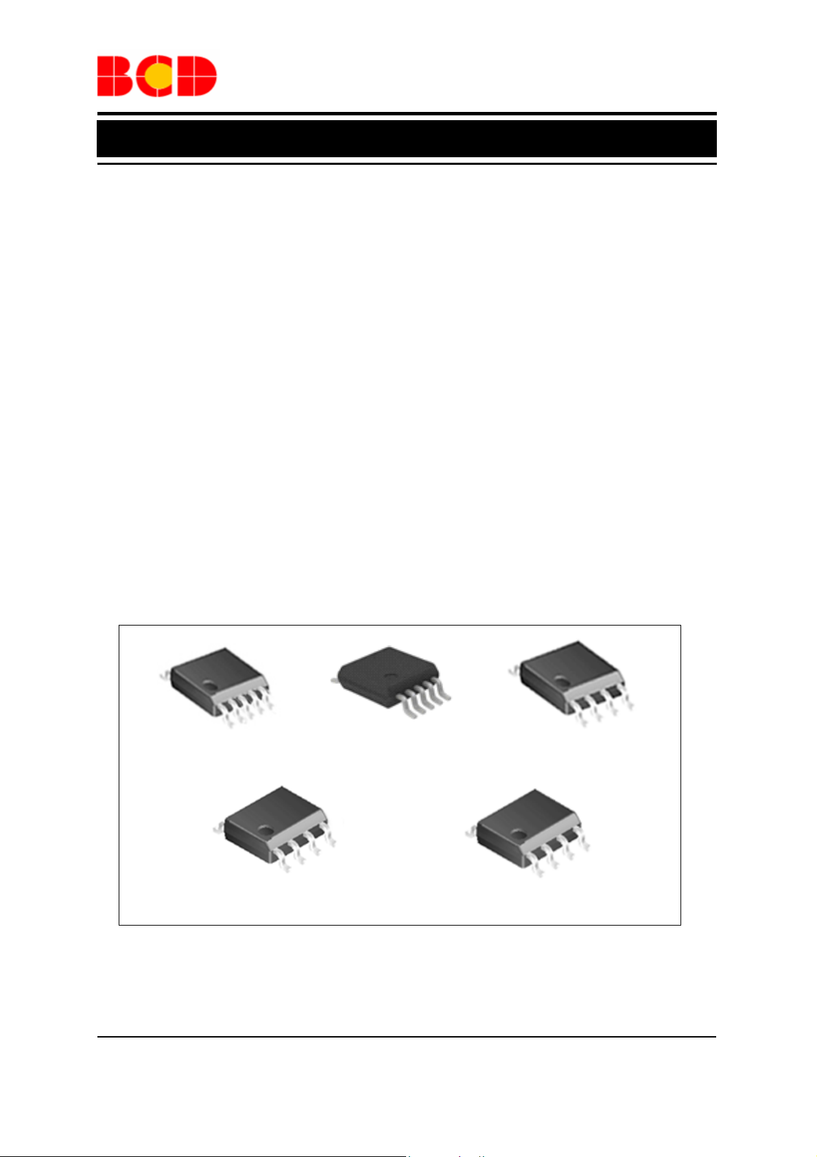
The AM4953 is available in MSOP-10, SSOP-10,
MSOP-8, SOIC-8 and PSOP-8 packages.
Features
• BTL Output Single-phase Full-wave Linear
Drive (Gain Resistor=1k to 360kΩ, Gain=51dB)
• Support Low-voltage Drive and Feature a Wide
Usable Voltage Range (2.2V to 16V)
• Low Saturation Output (High Side and Low Side
Saturation Voltage): V
I
=300mA)
OUT
• Built-in Lock Protection and Automatic Restart
Circuits
• Built-in FG/RD Output
• Built-in Hall Sensor Bias (V
• Thermal Protection Circuit
• Small-sized, High Thermal Capacity Package
SAT_TOTAL
=1.2V (typical,
=1.45V)
HB
Applications
• Notebook, Personal Computers
• Power Supplies in Consumer Electronics, Car
Audio
• CPU Cooling Systems
MSOP-10 SSOP-10 MSOP-8
SOIC-8 PSOP-8
Figure 1. Package Types of AM4953
Apr. 2012 Rev. 1. 5 BCD Semiconductor Manufacturing Limited
1
Page 2

Data Sheet
BTL Drive Single-phase Full-wave Fan Motor Driver AM4953
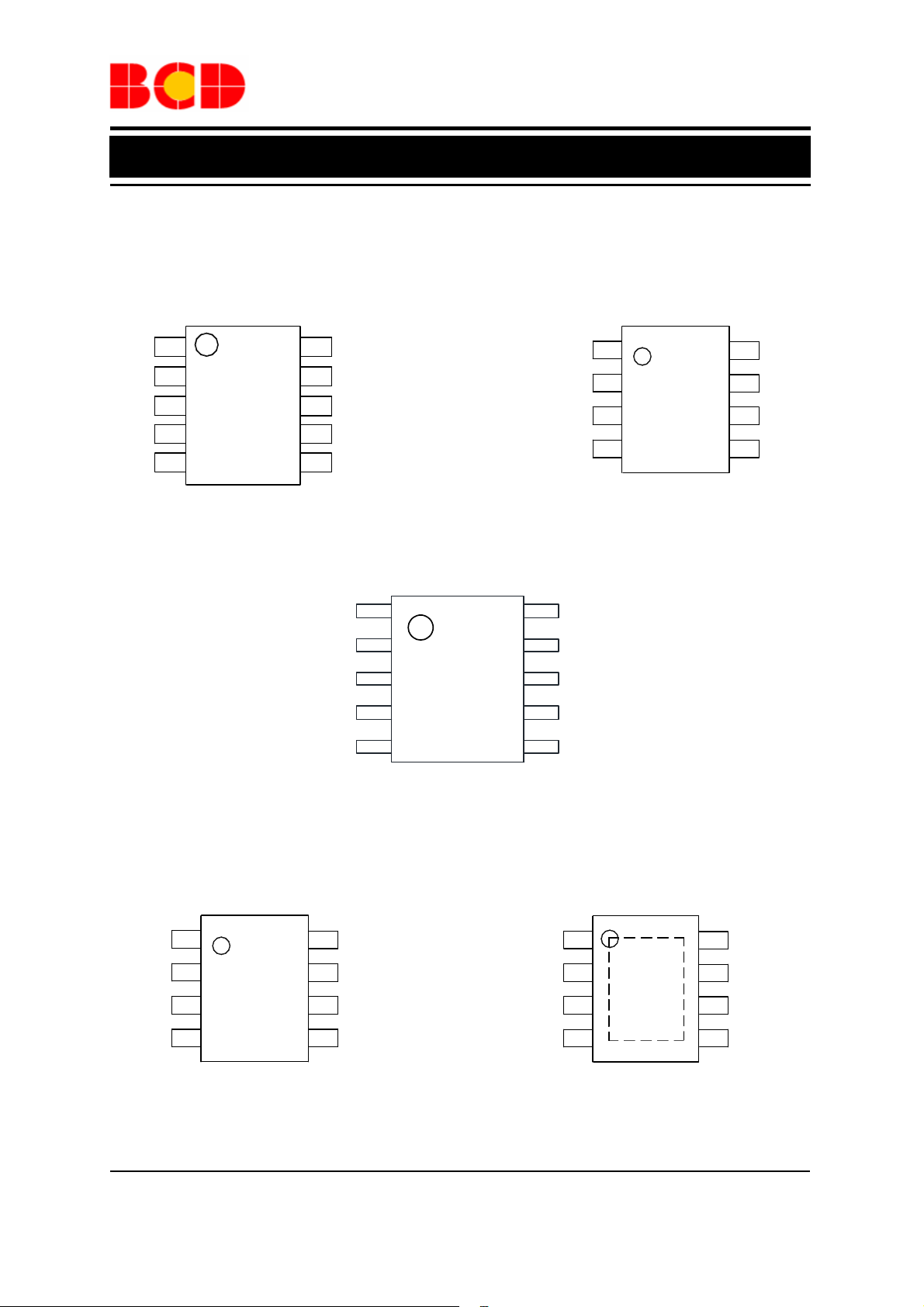
Pin Configuration
MM Package M8 Package
(MSOP-10) (MSOP-8)
IN+
HB
INCT
OUT1
IN+
IN-
CT
OUT1
1
2
3
4
5
10
RD
FG
9
VCC
8
OUT2
7
GND
6
GS Package
(SSOP-10)
1
IN+
HB
2
IN-
3
CT
4
OUT1
5
M Package MP Package
(SOIC-8) (PSOP-8)
8
1
2
7
FG/RD
VCC
OUT2
3
6
GND
4
5
Figure 2. Pin Configuration of AM4953 (Top View)
IN+
1
IN-
2
3
CT
RD
FG
VCC
OUT2
GND
1
2
3
4
4
8
7
6
5
OUT1
10
9
8
7
6
IN+
IN-
CT
OUT1
8
7
6
5
FG
VCC
OUT2
GND
RD
VCC
OUT2
GND
Apr. 2012 Rev. 1. 5 BCD Semiconductor Manufacturing Limited
2
Page 3

Data Sheet
BTL Drive Single-phase Full-wave Fan Motor Driver AM4953
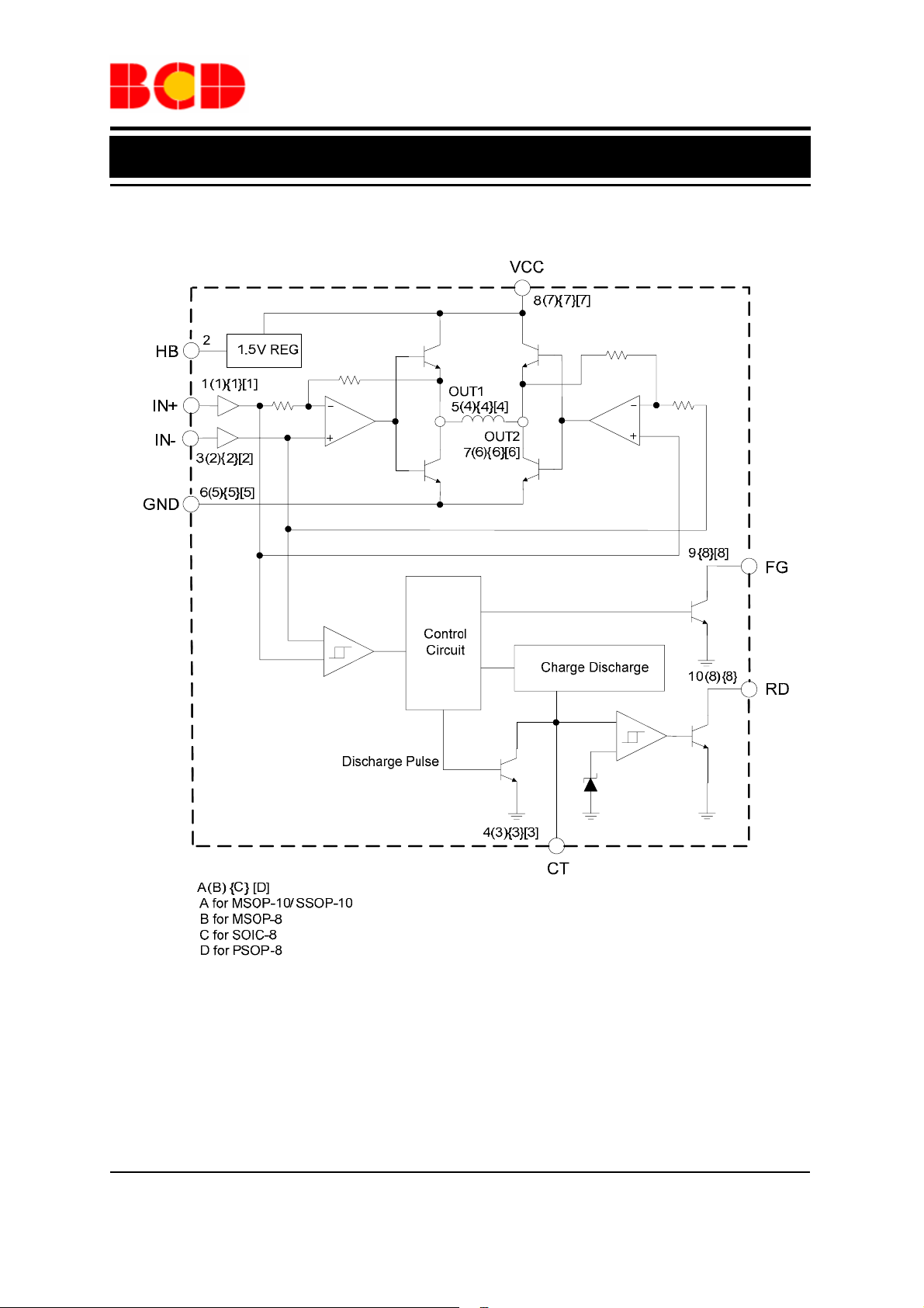
Functional Block Diagram
Figure 3. Functional Block Diagram of AM4953
Apr. 2012 Rev. 1. 5 BCD Semiconductor Manufacturing Limited
3
Page 4

Data Sheet
BTL Drive Single-phase Full-wave Fan Motor Driver AM4953
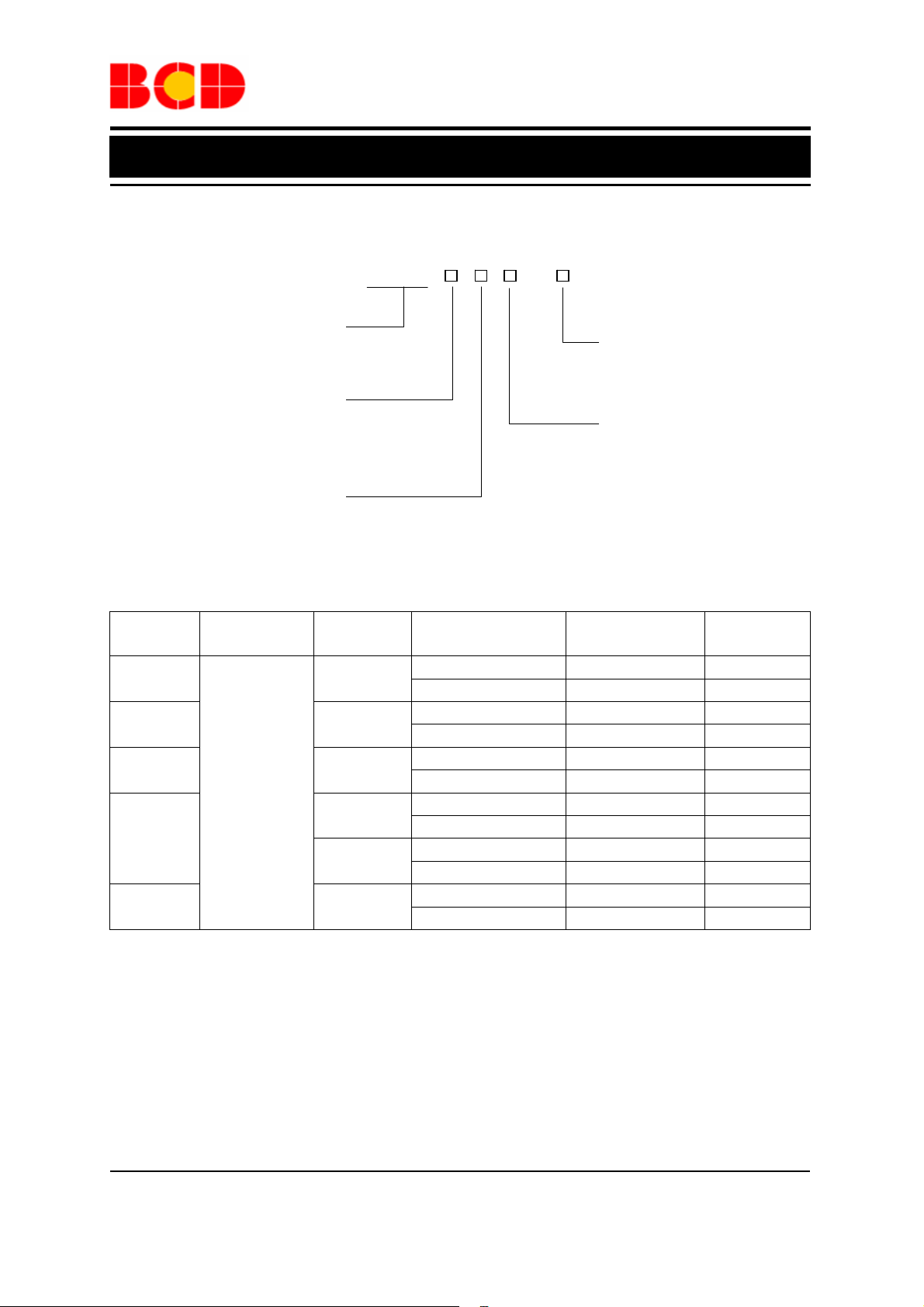
Ordering Information
AM4953 -
Circuit Type
Package
MSOP-10
SSOP-10 FG & RD
MSOP-8 RD
SOIC-8
PSOP-8 FG
BCD Semiconductor's Pb-free products, as designated with "G1" suffix in the part number, are RoHS compliant
and green.
Output Signal:
Blank: FG&RD/RD
F: FG
Package:
MM: MSOP-10
GS : SSOP-10
M8: MSOP-8
M: SOIC-8
MP: PSOP-8
Temperature
Range
FG & RD
-40 to 105ºC
Output
Signal
RD
FG
G1: Green
TR: Tape & Reel
Blank: Tube
Part Number Marking ID
AM4953MM-G1 4953MM-G1 Tube
AM4953MMTR-G1 4953MM-G1 Tape & Reel
AM4953GS-G1 4953GS-G1 Tube
AM4953GSTR-G1 4953GS-G1 Tape & Reel
AM4953M8-G1 4953M8-G1 Tube
AM4953M8TR-G1 4953M8-G1 Tape & Reel
AM4953M-G1 4953M-G1 Tube
AM4953MTR-G1 4953M-G1 Tape & Reel
AM4953FM-G1 4953FM-G1 Tube
AM4953FMTR-G1 4953FM-G1 Tape & Reel
AM4953FMP-G1 4953FMP-G1 Tube
AM4953FMPTR-G1 4953FMP-G1 Tape & Reel
Packing
Type
Apr. 2012 Rev. 1. 5 BCD Semiconductor Manufacturing Limited
4
Page 5

Data Sheet
BTL Drive Single-phase Full-wave Fan Motor Driver AM4953
Absolute Maximum Ratings (Note 1, TA=25ºC)
Parameter Symbol
Supply Voltage VCC 20 V
Peak Output Current I
FG/RD Pull-up Voltage VFG/VRD 15 V
FG/RD Output Current IFG/IRD 10 mA
Thermal Resistance
(Junction to Ambient)
Thermal Resistance
(Junction to Case)
Power Dissipation PD
Operating T em perature TOP -40 to 125 ºC
Storage Temperature T
ESD (Human Body Model) ESD 4000 V
ESD (Machine Model) ESD 200 V
800 mA
OUT
MSOP-10 195
MSOP-8 205
θ
JA
θ
JC
-55 to 150 ºC
STG
SSOP-10 155
SOIC-8 160
PSOP-8 110
MSOP-10 46
MSOP-8 48
SSOP-10 39
SOIC-8 40
PSOP-8 36
MSOP-10
MSOP-8
SSOP-10 800
SOIC-8 780
PSOP-8 960
Note 1: Stresses greater than those listed under “Absolute Maximu m Ratings” may cause permanent damage to
the device. These are stress ratings only, and functional operation of the device at these or any other conditions
beyond those indicated under “Recommended Operating Conditions” is not implied. Exposure to “Absolute
Maximum Ratings” for extended periods may affect device reliability.
Value
Unit
°C/W
°C/W
585
mW
Recommended Operating Conditions
Parameter Symbol Min Max Unit
Supply Voltage VCC 2.2 16 V
Hall Input Voltage V
Operating Ambient Temperature TA -40 105 ºC
Apr. 2012 Rev. 1. 5 BCD Semiconductor Manufacturing Limited
0 VCC-1.5 V
ICM
5
Page 6

Data Sheet
BTL Drive Single-phase Full-wave Fan Motor Driver AM4953
Electrical Characteristics
VCC=12V, TA=25oC, unless otherwise specified.
Parameter Symbol Conditions Min Typ Max Unit
I
VCT=L 6 8 9.6 mA
Supply Current
CT Charge Current I
CC1
I
VCT=H 2 4 6 mA
CC2
1 1.7 2.5
CHG
µA
CT Discharge Current I
CT Charge/Discharge
Current Ratio
CT Clamp Voltage VCL 1.25 1.45 1.65 V
CT Comparator Voltage VCP 0.25 0.45 0.65 V
OUT Low Saturation Voltage V
OUT High Saturation Voltage V
Hall Input Sensitivity VHN 8 20 mV
FG Low Level Voltage VFG IFG=5mA 0.15 0.3 V
FG Leakage Current I
RD Low Level Voltage VRD IRD=5mA 0.15 0.3 V
RD Leakage Current I
HB Voltage VHB IHB=5mA 1.3 1.45 1.6 V
0.15 0.27 0.36
DHG
I
R
CT
I
SAT_L
I
SAT_H
VFG=15V 1 10
FGL
VRD=15V 1 10
RDL
/ I
CHG
OUT
OUT
5 7 10
DHG
=300mA 0.25 0.45 V
=300mA 0.95 1.3 V
µA
µA
µA
Apr. 2012 Rev. 1. 5 BCD Semiconductor Manufacturing Limited
6
Page 7

Data Sheet
BTL Drive Single-phase Full-wave Fan Motor Driver AM4953
Typical Performance Characteristics
10
8
6
(mA)
CC
I
4
2
TA=25oC
0
0 5 10 15 20
VCC (V)
I
CC1
I
CC2
(VCT=L)
(VCT=H)
14
12
10
8
(mA)
CC
6
I
4
2
0
-40
-25 0 25 50 75 100 125
TA (oC)
VCC=12V
I
I
(VCT=L)
CC1
(VCT=H)
CC2
Figure 4. ICC vs. VCC Figure 5. ICC vs. TA
2.0
(V)
SAT
V
1.6
1.2
0.8
VCC=12V,TA=25oC
V
SATH
V
SATL
0.4
0.0
0 200 400 600 800
I
(mA)
OUT
800
700
600
500
400
(mW)
D
P
300
200
100
0
-40
-25 0 25 50 75 100 125 150
Package: MSOP-10/MSOP-8
TA (oC)
Figure 6. V
SAT
vs. I
Figure 7. PD vs.TA
OUT
Apr. 2012 Rev. 1. 5 BCD Semiconductor Manufacturing Limited
7
Page 8

Data Sheet
BTL Drive Single-phase Full-wave Fan Motor Driver AM4953
Typical Performance Characteristics (Continued)
1000
800
600
(mW)
D
P
400
200
0
-25 0 25 50 75 100 125 150
Package: SSOP-10
TA (oC)
900
750
600
450
300
Power Dissipation (mW)
150
0
-50 -25 0 25 50 75 100 125 150
Ambient Temperature (OC)
Package: SOIC-8
Figure 8. PD vs.TA Figure 9. PD vs.TA
1200
1050
900
750
600
450
Power Dissipation (mW)
300
150
0
-50 -25 0 25 50 75 100 125 150
Ambient Temperature (OC)
Package: PSOP-8
Figure 10. PD vs.T
A
Apr. 2012 Rev. 1. 5 BCD Semiconductor Manufacturing Limited
8
Page 9

Data Sheet
BTL Drive Single-phase Full-wave Fan Motor Driver AM4953
Truth Table
Items IN- IN+ CT OUT1 OUT2 FG RD Mode
1 H L
L
2 L H L H H
3 H Off OFF H
H L L
L Purring Rotation
Lock Protection
Apr. 2012 Rev. 1. 5 BCD Semiconductor Manufacturing Limited
9
Page 10

Data Sheet
BTL Drive Single-phase Full-wave Fan Motor Driver AM4953
Typical Application
V
HALL
C2
IN+
IN-
AM4953
CT
OUT1
HB
RD
FG
VCC
OUT2
GND
V
C1
(Note 2)
RD
R1
(Note 4)
FG
R2
D1
L
V
V
FG
RD
D1
C1
(Note 5)
R3
AH921
(Note 4)
VCC
HB
IN-
AM4953
IN+
CT
C2
RD
FG
OUT1
OUT2
GND
R1
(Note 4)
R2
L
Note 2: Adding D1 can protect the IC from destruction by reverse connection. If D1 is used, it is necessary to
insert a capacitor C1 to provide a regenerative current route. Similarly, if there is no nearby capacitor on the fan
power supply line, C1 will also be necessary to improve reliability. Its capacity should be larger than 2.2µF.
Note 3: If the line between Hall sensor output and Hall sensor input of IC is long, the noise may occur in this line.
But it can be eliminated by adding a capacitor C3.
Note 4: Each of R1 and R2 is recommended to be 51kΩ typical. R3 is recommended to be 2k and must be added
when V
Note 5: The package of AH921 is SOT-23-3. If it is packaged in TO-92S-3,please exchange IN- with IN+.
is larger than 20V.
CC
Figure 11. Typical Application of AM4953
Apr. 2012 Rev. 1. 5 BCD Semiconductor Manufacturing Limited
10
Page 11

Data Sheet
BTL Drive Single-phase Full-wave Fan Motor Driver AM4953
Mechanical Dimensions
MSOP-10 Unit: mm(inch)
Apr. 2012 Rev. 1. 5 BCD Semiconductor Manufacturing Limited
11
Page 12

Data Sheet
BTL Drive Single-phase Full-wave Fan Motor Driver AM4953
Mechanical Dimensions (Continued)
SSOP-10 Unit: mm(inch)
1.350(0.053)
3.800(0.150)
4.000(0.157)
1.550(0.061)
0.300(0.012)
0.450(0.018)
0.170(0.007)
0.250(0.010)
5.800(0.228)
6.200(0.244)
0.400(0.016)
1.270(0.050)
4.700(0.185)
5.100(0.201)
0
8
1.000(0.039)
BSC
0.100(0.004)
0.250(0.010)
1.350(0.053)
1.750(0.069)
Apr. 2012 Rev. 1. 5 BCD Semiconductor Manufacturing Limited
12
Page 13

Data Sheet
BTL Drive Single-phase Full-wave Fan Motor Driver AM4953
Mechanical Dimensions (Continued)
MSOP-8 Unit: mm(inch)
Apr. 2012 Rev. 1. 5 BCD Semiconductor Manufacturing Limited
13
Page 14

Data Sheet
BTL Drive Single-phase Full-wave Fan Motor Driver AM4953
Mechanical Dimensions (Continued)
4.700(0.185)
5.100(0.201)
7
°
SOIC-8 Unit: mm(inch)
1.350(0.053)
1.750(0.069)
0.320(0.013)
°
8
1.000(0.039)
7
°
1.270(0.050)
TYP
0.330(0.013)
0.510(0.020)
0.100(0.004)
0.300(0.012)
3.800(0.150)
4.000(0.157)
0.190(0.007)
0.250(0.010)
0.900(0.035)
0.675(0.027)
0.725(0.029)
R0.150(0.006)
D
0
°
8
°
1°
5°
5.800(0.228)
6.200(0.244)
D
1
:
0
2
0.450(0.017)
0.800(0.031)
5
1
.
0
R
°
8
0.800(0.031)
0.200(0.008)
)
6
0
0
.
0
(
0
Note: Eject hole, oriented hole and mold mark is optional.
Apr. 2012 Rev. 1. 5 BCD Semiconductor Manufacturing Limited
14
Page 15

Data Sheet
BTL Drive Single-phase Full-wave Fan Motor Driver AM4953
Mechanical Dimensions (Continued)
PSOP-8 Unit: mm(inch)
3.202(0.126)
3.402(0.134)
Apr. 2012 Rev. 1. 5 BCD Semiconductor Manufacturing Limited
15
Page 16

BCD Semiconductor Manufacturing Limited
IMPORTANT NOTICE
http://www.bcdsemi.com
BCD Semiconductor Manufacturing Limited reserves the right to make changes without further notice to any products or specifications herein. BCD Semiconductor Manufacturing Limited does not assume any responsibility for use of any its products for any
IMPORTANT NOTICE
IMPORTANT NOTICE
particular purpose, nor does BCD Semiconductor Manufacturing Limited assume any liability arising out of the application or use
of any its products or circuits. BCD Semiconductor Manufacturing Limited does not convey any license under its patent rights or
BCD Semiconductor Manufacturing Limited reserves the right to make changes without further notice to any products or specifi-
BCD Semiconductor Manufacturing Limited reserves the right to make changes without further notice to any products or specifi-
other rights nor the rights of others.
cations herein. BCD Semiconductor Manufacturing Limited does not assume any responsibility for use of any its products for any
cations herein. BCD Semiconductor Manufacturing Limited does not assume any responsibility for use of any its products for any
particular purpose, nor does BCD Semiconductor Manufacturing Limited assume any liability arising out of the application or use
particular purpose, nor does BCD Semiconductor Manufacturing Limited assume any liability arising out of the application or use
MAIN SITE
of any its products or circuits. BCD Semiconductor Manufacturing Limited does not convey any license under its patent rights or
of any its products or circuits. BCD Semiconductor Manufacturing Limited does not convey any license under its patent rights or
- Headquarters
BCD (Shanghai) Micro-electronics Limited
other rights nor the rights of others.
other rights nor the rights of others.
No. 1600, Zi Xing Road, Shanghai ZiZhu Science-based Industrial Park, 200241, P. R.C.
Tel: +86-021-2416-2266, Fax: +86-021-2416-2277
MAIN SITE
MAIN SITE
REGIONAL SALES OFFICE
- Headquarters
BCD Semiconductor Manufacturing Limited
BCD Semiconductor Manufactur ing Limited
Shenzhen Office
- Wafer Fab
No. 1600, Zi Xing Road, Shanghai ZiZhu Science-based Industrial Park, 200241, China
Shanghai SIM-BCD Semiconductor Manufacturing Co., Ltd., Shenzhen Office
Shanghai SIM-BCD Semiconductor Manufacturing Limited
Tel: +86-21-24162266, Fax: +86-21-24162277
Unit A Room 1203,Skyworth Bldg., Gaoxin Ave.1.S., Nanshan District
800, Yi Shan Road, Shanghai 200233, China
Shenzhen 518057, China
Tel: +86-21-6485 1491, Fax: +86-21-5450 0008
REGIONAL SALES OFFICE
Tel: +86-0755-8660-4900, Fax: +86-0755-8660-4958
Shenzhen Office
REGIONAL SALES OFFICE
Shanghai SIM-BCD Semiconductor Manufacturing Co., Ltd., Shenzhen Office
Taiwan Office (Hsinchu)
Shenzhen Office
Unit A Room 1203, Skyworth Bldg., Gaoxin Ave.1.S., Nanshan District, Shenzhen,
BCD Semiconductor (Taiwan) Company Limited
Shanghai SIM-BCD Semiconductor Manufacturing Co., Ltd. Shenzhen Office
China
8F, No.176, Sec. 2, Gong-Dao 5th Road, East District
Advanced Analog Circuits (Shanghai) Corporation Shenzhen Office
Tel: +86-755-8826 7951
HsinChu City 300, Taiwan, R.O.C
Room E, 5F, Noble Center, No.1006, 3rd Fuzhong Road, Futian District, Shenzhen 518026, China
Fax: +86-755-8826 7865
Tel: +886-3-5160181, Fax: +886-3-5160181
Tel: +86-755-8826 7951
Fax: +86-755-8826 7865
- Wafer Fab
Shanghai SIM-BCD Semiconductor Manufacturing Co., Ltd.
800 Yishan Road, Shanghai 200233, China
Tel: +021-6485-1491, Fax: +86-021-5450-0008
- Wafer Fab
BCD Semiconductor Manufacturing Limited
Shanghai SIM-BCD Semiconductor Manufacturing Co., Ltd.
Taiwan Office (Taipei)
- IC Design Group
800 Yi Shan Road, Shanghai 200233, China
BCD Semiconductor (Taiwan) Company Limited
Advanced Analog Circuits (Shanghai) Corporation
Tel: +86-21-6485 1491, Fax: +86-21-5450 0008
3F, No.17, Lane 171, Sec. 2, Jiu-Zong Rd., Nei-Hu Dist., Taipei(114), Taiwan, R.O.C
8F, Zone B, 900, Yi Shan Road, Shanghai 200233, China
Tel: +886-2-2656 2808
Tel: +86-21-6495 9539, Fax: +86-21-6485 9673
Fax: +886-2-2656-2806/26562950
Taiwan Office
BCD Semiconductor (Taiwan) Company Limited
USA Office
Taiwan Office
4F, 298-1, Rui Guang Road, Nei-Hu District, Taipei,
BCD Semiconductor Corp.
BCD Semiconductor (Taiwan) Company Limited
Tai wan
48460 Kato Road, Fremont, CA 94538, USA
4F, 298-1, Rui Guang Road, Nei-Hu District, Taipei,
Tel: +886-2-2656 2808
Tel: +1-510-668-1950
Taiwan
Fax: +886-2-2656 2806
Fax: +1-510-668-1990
Tel: +886-2-2656 2808
Fax: +886-2-2656 2806
USA Office
Korea Office
BCD Semiconductor Limited Korea office.
Room 101-1112, Digital-Empire II, 486 Sin-dong,
Yeongtong-Gu, Suwon-city, Gyeonggi-do, Korea
Tel: +82-31-695-8430
BCD Semiconductor Corp.
USA Office
30920 Huntwood Ave. Hayward,
BCD Semiconductor Corporation
CA 94544, USA
30920 Huntwood Ave. Hayward,
Tel : +1-510-324-2988
CA 94544, U.S.A
Fax: +1-510-324-2788
Tel : +1-510-324-2988
Fax: +1-510-324-2788
 Loading...