

Page 1
A
Description
L9910/ AL9910A/ AL9910-5/AL9910A-5
UNIVERSAL HIGH VOLTAGE HIGH BRIGHTNESS LED DRIVER
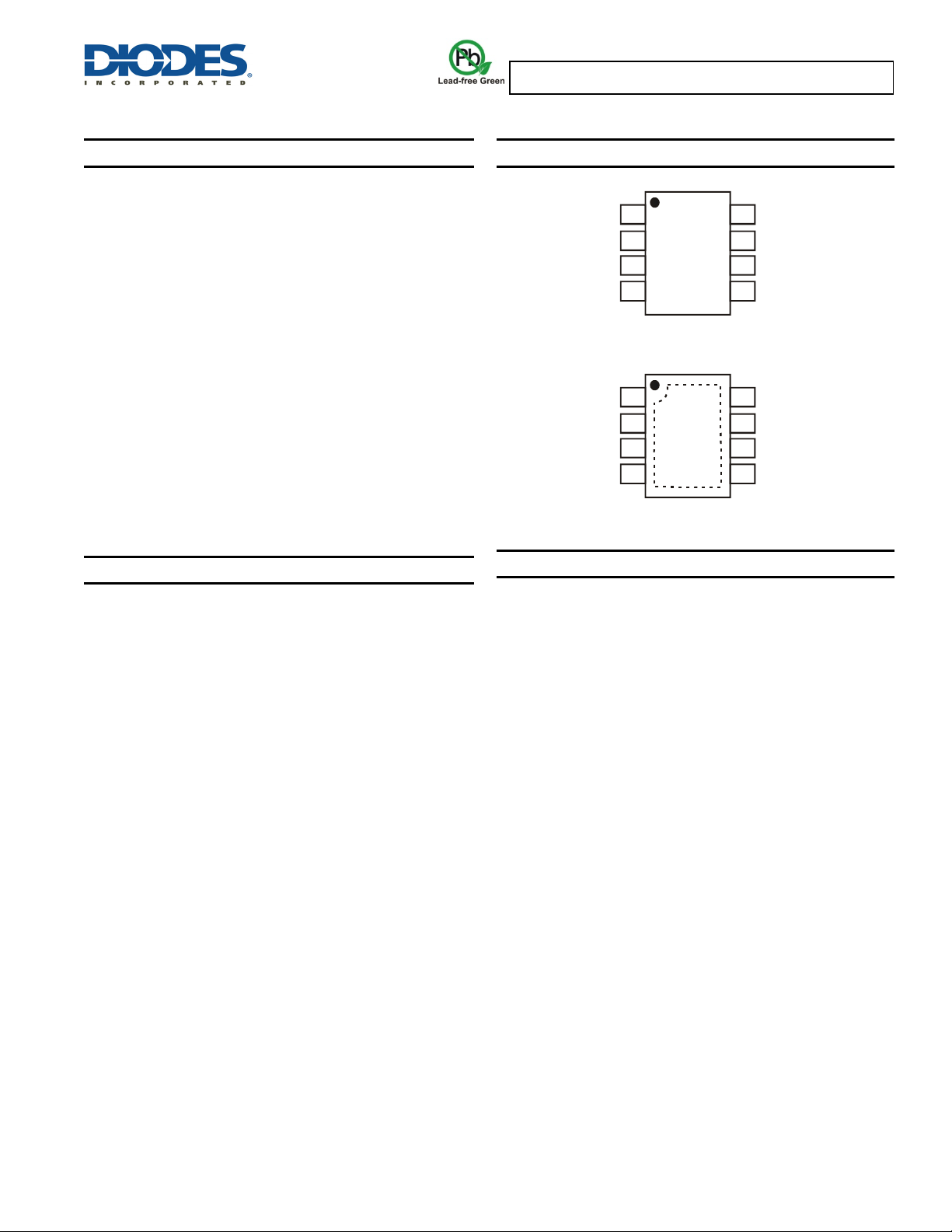
Pin Assignments
IN
IN
(Top View)
1
2
AL9910
3
4
SO-8
(Top View)
1
2
AL9910
3
4
SO-8EP
R
8
OSC
7
LD
V
6
DD
5
PWM_D
R
8
OSC
7
LD
V
6
DD
5
PWM_D
The AL9910/A high voltage PWM LED driver-controller provides an
efficient solution for offline high brightness LED lamps from rectified
line voltages ranging from 85V
external MOSFETs at switching frequencies up to 300kHz, with the
switching frequency determined by a single resistor. The AL9910
topology creates a constant current through the LEDs providing
constant light output. The output current is programmed by one
external resistor and is ultimately determined by the external
MOSFET chosen and therefore allows many low current LEDs to be
driven as well as a few high current LEDs.
The LED brightness can be varied by both Linear and PWM dimming
using the AL9910’s LD and PWM_D pins respectively. The PWM_D
input operates with duty ratio of 0-100% and frequency of up to
several kHz.
The AL9910 can withstand input voltages up to 500V which makes it
very resilient to transients at standard mains voltages. As well as
standard SO-8 package the AL9910 is available in the thermally
enhanced SO-8EP package.
Features
• >90% Efficiency
• Universal Rectified 85 to 277V
• Input Voltage Up to 500V
• Internal Voltage Regulator Removes Start-Up Resistor
7.5V MOSFET Drive – AL9910
10V MOSFET Drive – AL9910A
• Tighter Current Sense Tolerance: 5% AL9910-5, AL9910A-5
• Drives LED Lamps with Both High and Low Current LEDs
• LED Brightness Control with Linear and PWM Dimming
• Internal Thermal Protection (OTP)
• Available in SO-8 and SO-8EP Packages
• Totally Lead-Free & Fully RoHS Compliant (Notes 1 & 2)
• Halogen and Antimony Free. “Green” Device (Note 3)
Notes: 1. No purposely added lead. Fully EU Directive 2002/95/EC (RoHS) & 2011/65/EU (RoHS 2) compliant.
2. See http://www.diodes.com/quality/lead_free.html for more information about Diodes Incorporated’s definitions of Halogen- and Antimony-free, "Green"
and Lead-free.
3. Halogen- and Antimony-free "Green” products are defined as those which contain <900ppm bromine, <900ppm chlorine (<1500ppm total Br + Cl) and
<1000ppm antimony compounds.
up to 277VAC. The AL9910 drives
AC
Input Range
AC
Applications
• LED Offline Lamps
• High Voltage DC-DC LED Driver
• Signage and Decorative LED Lighting
• Back Lighting of Flat Panel Displays
• General Purpose Constant Current Source
V
CS
GND
GATE
V
CS
GND
GATE
AL9910/ AL9910A/ AL9910-5/ AL9910-5A
Document number: DS35103 Rev. 9 - 2
1 of 15
www.diodes.com
May 2014
© Diodes Incorporated
Page 2
A
L9910/ AL9910A/ AL9910-5/AL9910A-5
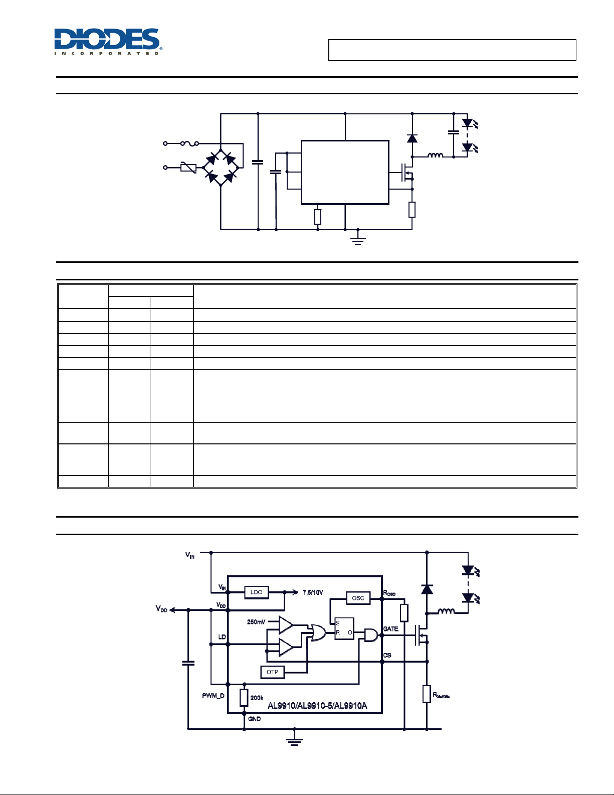
Typical Applications Circuit
C3
C3
D1
VACIN
VACIN
BR1
BR1
C1
C1
C2
C2
V
V
LD
LD
PWM_D
PWM_D
R
R
OSC
OSC
DD
DD
AL9910/A
AL9910/A
R
R
OSC
OSC
V
V
IN
IN
GND
GND
GATE
GATE
CS
CS
Q1
Q1
R
R
D1
SENSE
SENSE
L1
L1
Pin Descriptions
Pin
Name
VIN
SO-8 SO-8EP
Pin Number
1 1
Input Voltage
Function
CS 2 2 Senses LED string and external MOSFET switch current
GND 3 3 Device Ground
Gate 4 4 Drives the gate of the external MOSFET switch.
PWM_D 5 5 Low Frequency PWM Dimming pin, also Enable input. Internal 200kΩ pull-down to GND.
Internally regulated supply voltage.
7.5V nominal for AL9910 and AL9910-5
10V nominal for AL9910A.
VDD
6 6
Can supply up to 1 mA for external circuitry. A sufficient storage capacitor is used to provide storage when
the rectified AC input is near the zero crossing.
LD 7 7
Linear Dimming Input. Changes the current limit threshold at current sense comparator and changes the
average LED current.
Oscillator Control. A resistor connected between this pin and ground sets the PWM frequency. The devices
R
OSC
8 8
can be switched into constant off time (PFM) mode by connecting the external oscillator resistor between
pin and the gate of the external MOSFET.
R
OSC
EP PAD N/A EP Exposed Pad (bottom). Connect to GND directly underneath the package.
Functional Block Diagram
AL9910/ AL9910A/ AL9910-5/ AL9910-5A
Document number: DS35103 Rev. 9 - 2
2 of 15
www.diodes.com
May 2014
© Diodes Incorporated
Page 3
A
L9910/ AL9910A/ AL9910-5/AL9910A-5
Absolute Maximum Ratings (Note 4) (@T
= +25°C, unless otherwise specified.)
A
Symbol Parameter Ratings Unit
V
Maximum input voltage, VIN, to GND
IN(MAX)
VCS
VLD
V
PWM_D
V
GATE
V
DD(MAX)
Maximum CS input pin voltage relative to GND -0.3 to +0.45 V
Maximum LD input pin voltage relative to GND
Maximum PWM_D input pin voltage relative to GND
Maximum GATE pin voltage relative to GND
Maximum VDD pin voltage relative to GND
Continuous Power Dissipation (T
SO-8 (derate 6.3mW/°C above +25°C)
= +25°C)
A
-0.5 to +520 V
-0.3 to (VDD +0.3)
-0.3 to (VDD +0.3)
-0.3 to (VDD +0.3)
12 V
630 mW
V
V
V
SO-8EP (derate at 22mW/°C above 25°C) 2200 mW
TJ
TST
Junction Temperature Range +150 °C
Storage Temperature Range -65 to +150 °C
ESD HBM Human Body Model ESD Protection (Note 5) 1500 V
ESD MM Machine Model ESD Protection (Note 5) 300 V
Notes: 4. Stresses above those listed under Absolute Maximum Ratings may cause permanent damage to the device. This is a stress rating only; functional
operation of the device at these or any other conditions above those listed in the operational sections of this specification is not implied. Exposure
to absolute maximum rating conditions for extended periods may affect device reliability.
All voltages are with respect to Ground. Currents are positive into, negative out of the specified terminal.
5. Semiconductor devices are ESD sensitive and may be damaged by exposure to ESD events. Suitable ESD precautions should be taken when
handling and transporting these devices
Recommended Operating Conditions (@T
= +25°C, unless otherwise specified.)
A
Symbol Parameter Min Max Unit
AL9910
V
Input DC Supply Voltage Range
INDC
AL9910-5
AL9910A
Al9910A-5
Ambient Temperature Range (Note 6)
TA
AL9910_S
AL9910_SP -40 +105
AL9910
VDD Maximum Recommended Voltage Applied to VDD Pin (Note 7)
AL9910-5
AL9910A
AL9910A-5
V
EN(LO)
V
Notes: 6. Maximum ambient temperature range is limited by allowable power dissipation. The Exposed pad SO-8EP with its lower thermal impedance allows
the variants using this package to extend the allowable maximum ambient temperature range.
7. When using the AL9910 in isolated LED lamps an auxiliary winding might be used.
Pin PWM_D Input Low Voltage
Pin PWM_D Input High Voltage
EN(HI)
15.0 500
20.0 500
-40 +85
10
12
0 1
2.4
VDD
V
°C
V
V
AL9910/ AL9910A/ AL9910-5/ AL9910-5A
Document number: DS35103 Rev. 9 - 2
3 of 15
www.diodes.com
May 2014
© Diodes Incorporated
Page 4
A
L9910/ AL9910A/ AL9910-5/AL9910A-5
Electrical Characteristics (@T
= +25°C, unless otherwise specified.)
A
Symbol Parameter Conditions Min Typ Max Unit
I
INSD
VDD
I
DD(ext)
UVLO
Shut-Down Mode Supply Current
Internally Regulated Voltage
Current Available for External
V
DD
Circuitry
V
Under Voltage Lockout Threshold V
DD
Pin PWM_D to GND,
V
IN
V
IN
l
DD(ext)
V
IN
DD
= V
= V
= V
rising
(Note 6)
IN(MIN)
~500V, (Note 8)
IN(MIN)
= 0, Gate pin open
to 100V (Notes 8 & 9)
IN(MIN)
AL9910
AL9910-5
AL9910A
AL9910
AL9910-5
AL9910A 9 10 11
AL9910
AL9910-5
0.50 1
0.65
1.2
7.0 7.5 8.0
1.0 mA
6.4 6.7 7
mA
V
V
AL9910A 8 9 10
∆UVLO
V
Under Voltage Lockout Hysteresis V
DD
falling
DD
AL9910
AL9910-5
500
mV
AL9910A 750
R
PWM_D
V
CS(HI)
PWM_D Pull-Down Resistance
Current Sense Threshold Voltage
V
= 5V
PWM_D
Full ambient temperature range
(Note 10)
AL9910
AL9910A
AL9910A-5
150 200 250 kΩ
225 250 275
230 255 280
mV
242 255 267
AL9910-5 237.5 250 262.5
V
GATE(HI)
V
GATE(LO)
f
D
t
BLANK
t
DELAY
t
t
T
Notes: 8. V
9. Also limited by package power dissipation limit, whichever is lower.
10. Full ambient temperature range for AL9910-5S, AL9910AS and AL9910S is -40 to +85°C; for AL9910-5SP, AL9910ASP and AL9910SP is
-40°C to +105°C.
11. Device mounted on FR-4 PCB (25mm x 25mm 1oz copper, minimum recommended pad layout on top. For better thermal performance, larger
copper pad for heat-sink is needed.
12. Device mounted on FR-4 PCB (51mm x 51mm 2oz copper, minimum recommended pad layout on top layer and thermal vias to bottom layer ground
plane. For better thermal performance, larger copper pad for heat-sink is needed.
GATE High Output Voltage
GATE Low Output Voltage
Oscillator Frequency
OSC
Maximum Oscillator PWM Duty Cycle
MAXhf
Linear Dimming Pin Voltage Range
VLD
Current Sense Blanking Interval
Delay From CS Trip to GATE lo
GATE Output Rise Time
RISE
GATE Output Fall Time
FALL
Thermal Shut Down
TSD
Thermal Shut Down Hysteresis
SDH
Thermal Resistance Junction-to-
θJA
Ambient
Thermal Resistance Junction-to-Case
θJC
for the AL9910 is 15V and for the AL9910A it is 20V.
IN(MIN)
I
= 10mA VDD -0.3
OUT
I
= -10mA
OUT
R
= 1MΩ
OSC
R
= 226kΩ
OSC
= 25kHz, at GATE,
f
PWMhf
CS to GND.
Full ambient temperature range (Note 10),
V
= 20V
IN
VCS = 0.45V, VLD = VDD
V
= 20V, VLD = 0.15,
IN
= 0 to 0.22V after T
V
CS
C
= 500pF
GATE
C
= 500pF
GATE
BLANK
0 0.3 V
20 25 30
80 100 120
100 %
0
160 250 440 ns
300 ns
30 50 ns
30 50 ns
150
50
SO-8 (Note 11) 110
SO-8EP (Note 12) 66
SO-8 (Note 11)
22
SO-8EP (Note 12) 9
VDD
-
250 mV
V
kHz
°C
°C/W
°C/W
AL9910/ AL9910A/ AL9910-5/ AL9910-5A
Document number: DS35103 Rev. 9 - 2
4 of 15
www.diodes.com
May 2014
© Diodes Incorporated
Page 5
A
5
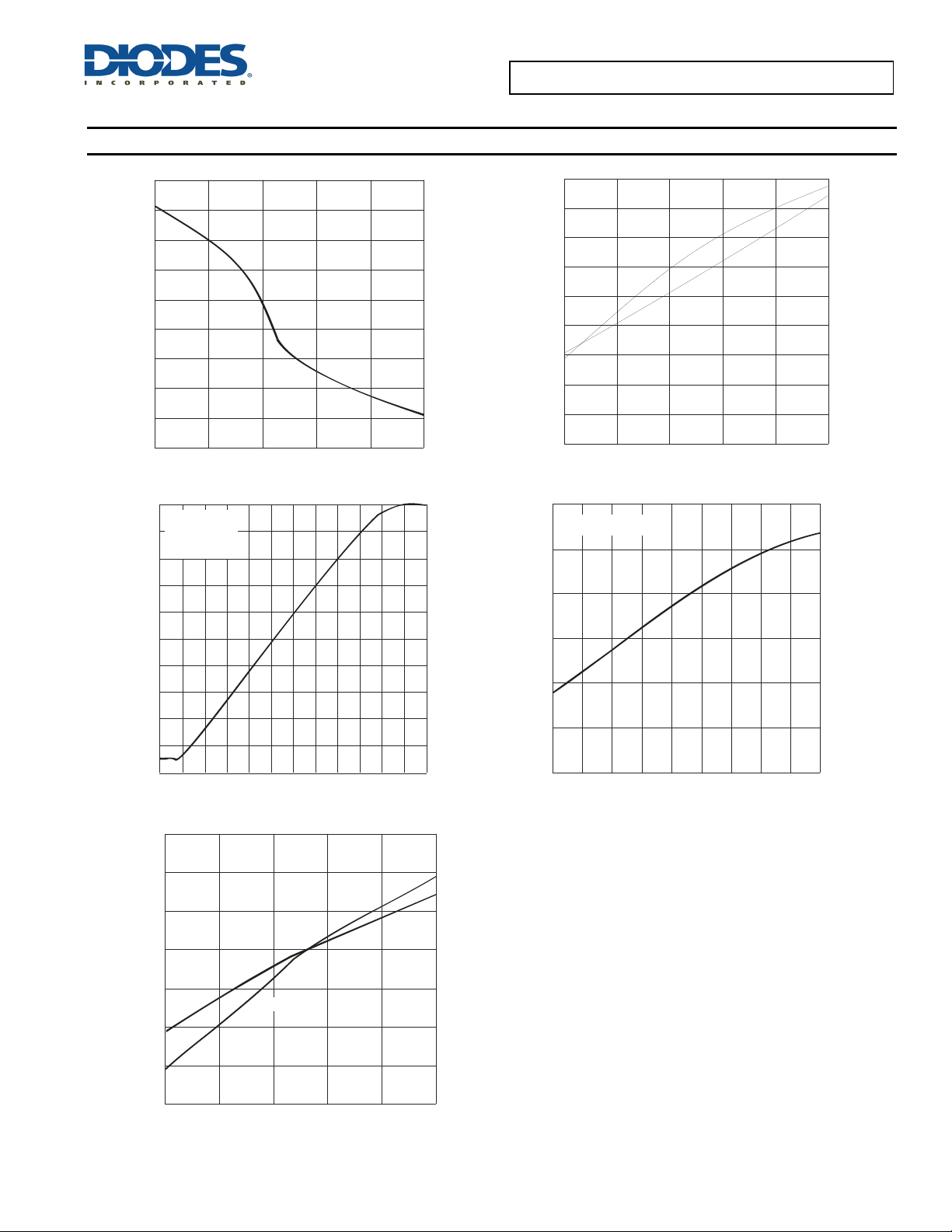
Typical Characteristics
3.0
2.5
2.0
L9910/ AL9910A/ AL9910-5/AL9910A-5
460
440
V = 400V
420
IN
1.5
1.0
0.5
0.0
-0.5
CURRENT SENS E THRESHOLD (mV)
-1.0
-1.5
-40 -15 10 35 60 85
AMBIE NT TEMP ER ATURE (°C)
Change in Current Sense Thresho ld vs. Ambient Temperatu re
100
I = 281mA
LED
90
V = 264V
IN
T = 23.5C
A
80
70
60
50
OUT MAX
I (%)
40
30
20
10
0
050
100 150 200 250 300
V DIMMING CONTROL (mV)
LD
I vs. V Dimming Control
OUT MAX LD
1.
400
V = 15V
IN
380
360
340
INPUT CURRENT (µA)
320
300
280
-40 -15 10 35 60 85
AMBIEN T TE MPE RATURE ( C)
°
Input Current vs. Ambient Temperatu re
450
I = 180mA
LED(NOM )
400
350
300
250
200
SHORT CIRCUIT OUTPUT CURRE NT (mA)
150
85 10 5 12 5 145 165 185 205 22 5
I NPUT V OLTAG E (V )
RMS
180mA LED Driver Short Ci rcu it Out put Current vs. I nput Voltage
245 26 5
1.0
0.5
0.0
R = 226k
OSC
Ω
-0.5
R = 1M
Ω
OSC
-1.0
CHANGE IN FREQUENCY (%)
-1.5
-2.0
-40 -15 10 35 60 85
AMBIE NT TEMPER ATURE ( °C)
Chan ge in Os cill ation Frequency vs. Ambie nt Temp erature
AL9910/ AL9910A/ AL9910-5/ AL9910-5A
Document number: DS35103 Rev. 9 - 2
5 of 15
www.diodes.com
May 2014
© Diodes Incorporated
Page 6

A
5
5
R
Typical Characteristics (cont.) measured using AL9910EV4
200
15 LEDs
190
14 LEDs
L9910/ AL9910A/ AL9910-5/AL9910A-5
9
18 LEDs
180
16 LEDs
170
OUT MAX
I (mA)
160
150
140
17 LEDs
18 LEDs
85 105 12 5 14 5 16 5 185 205 225 245 26 5
INPUT VOLTAGE (V )
RMS
180mA LED Driver Output Current vs. Input Voltage
0.9
18 LEDs
0.9
0.85
16 LEDs
0.8
POWER FACTO
15 LEDs
0.75
17 LEDs
90
17 LEDs
14 LEDs
EFFICIENCY (%)
85
80
105 125 145 165 185 205 225 245 26585
I NPUT V OLTAGE (V )
180mA LED Driver Efficiency vs. Inpu t Voltage
16 LEDs
15 LEDs
RMS
12
18 LEDs
17 LEDs
10
8
15 LEDs
POWER (W)
14 LEDs
16 LEDs
6
14 LEDs
0.7
85 105 12 5 14 5 165 18 5 20 5 225 245 26 5
INPUT VOLTAGE (V )
RMS
180mA L ED Driver Power Factor vs. In put Voltage
4
85 105 12 5 145 165 18 5 20 5 22 5 245 26 5
INPUT VOLTAGE (V )
RMS
180mA LED Driver Inp ut P ower Dissipation v s. Inp ut Voltage
AL9910/ AL9910A/ AL9910-5/ AL9910-5A
Document number: DS35103 Rev. 9 - 2
6 of 15
www.diodes.com
May 2014
© Diodes Incorporated
Page 7

A
L9910/ AL9910A/ AL9910-5/AL9910A-5
Application Information
The AL9910 is very versatile and is capable of operating in isolated or non-isolated topologies. It can also be made to operate in continuous as
well as discontinuous conduction mode.
V
V
IN
IN
V
V
IN
IN
V
V
DD
LD
LD
DD
V
V
DD
DD
LDO
LDO
250mV
250mV
OTP
OTP
7.5/10V
7.5/10V
OSC
OSC
S
S
RO
RO
R
R
OSC
OSC
GATE
GATE
CS
CS
R
PWM _D
PWM _D
100k
100k
GND
GND
AL9910/AL9910A
AL9910/AL9910A
R
SENSE
SENSE
Figure 1 Functional Block Diagram
The AL9910 contains a high voltage LDO (see Figure 1) the output of the LDO provides a power rail to the internal circuitry including the gate
driver. A UVLO on the output of the LDO prevents incorrect operation at low input voltage to the V
IN
pin.
In a non-isolated Buck LED driver when the gate pin goes high the external power MOSFET Q1 is turned on causing current to flow through the
LEDs, inductor (L1) and current sense resistor (R
). When the voltage across R
SENSE
exceeds the current sense pin threshold the external
SENSE
MOSFET Q1 is turned off. The stored energy in the inductor causes the current to continue to flow through the LEDs via diode D1.
The AL9910’s LDO provides all power to the rest of the IC including Gate drive this removes the need for large high power start-up resistors. This
means that operate correctly it requires around 0.5mA from the high voltage power rail. The LDO can also be used to supply up to 1mA to external
circuits.
The AL9910 operates and regulates by limiting the peak current of the external MOSFET; the peak current sense threshold is nominally set at
250mV.
The same basic operation is true for isolated topologies, however in these the energy stored in the transformer delivers energy to LEDs during the
off-cycle of the external MOSFET.
Design Parameters
Setting the LED Current
In the non-isolated buck converter topology, figure 1, the average LED current is not the peak current divided by 2 - however, there is a certain
error due to the difference between the peak and the average current in the inductor. The following equation accounts for this error:
R
SENSE
=
()
mV250
+
RIPPLELED
.
))I*5.0(I
AL9910/ AL9910A/ AL9910-5/ AL9910-5A
Document number: DS35103 Rev. 9 - 2
7 of 15
www.diodes.com
May 2014
© Diodes Incorporated
Page 8

A
(
(
)
L9910/ AL9910A/ AL9910-5/AL9910A-5
Applications Information (cont.)
Setting Operating Frequency
The AL9910 is capable of operating over a 25 and 300 kHz switching frequency range. The switching frequency is programmed by connecting an
external resistor between R
osc
=
t
OSC
The switching frequency is the reciprocal of the oscillator period. Typical values for R
When driving smaller numbers of LEDs, care should be taken to ensure that t
switching frequency by increasing the R
When operating in buck mode the designer must keep in mind that the input voltage must be maintained higher than 2 times the forward voltage
drop across the LEDs. This limitation is related to the output current instability that may develop when the AL9910 operates at a duty cycle greater
than 0.5. This instability reveals itself as an oscillation of the output current at a sub-harmonic (SBO) of the switching frequency.
The best solution is to adopt the so-called constant off-time operation as shown in Figure 2. The resistor (R
default, to set operating frequency. To force the AL9910 to enter constant OFF time mode R
This will decrease the duty cycle from 50% by increasing the total period, t
25
pin and ground. The corresponding oscillator period is:
OSC
+
22R
µs with R
OSC
in kΩ
OSC
value. Reducing the switching frequency will also improve the efficiency.
V
V
IN
IN
OFF
ON
+ tON.
vary from 75kΩ to 1MΩ
OSC
> t
. The simplest way to do this is to reduce/limit the
BLANK
is connected to the gate of the external MOSFET.
OSC
) is, connected to ground by
OSC
V
V
DD
DD
LD
LD
PWM_D
PWM_D
R
R
OSC
OSC
The oscillator period equation above now defines the AL9910 off time, t
When using this mode the nominal switching frequency is chosen and from the nominal input and output voltages the off-time can be calculated:
⎛
V
⎜
1t ∗
OFF
From this the timing resistor, R
−=
⎜
V
⎝
⎞
1
)nom(OUT
⎟
⎟
f
OSC)nom(IN
⎠
, can be calculated:
OSC
Figure 2. Constant Off-Time Configuration
OFFOSC
V
V
IN
IN
AL9910/A
AL9910/A
GND
GND
.
OFF
)
GATE
GATE
CS
CS
R
R
OSC
OSC
Ω−∗=
Q1
Q1
)k(2225)µs(tR
Inductor Selection
The non-isolated buck circuit, Figure 1, is usually selected and it has two operation modes: continuous and discontinuous conduction modes. A
buck power stage can be designed to operate in continuous mode for load current above a certain level usually 15% to 30% of full load. Usually,
the input voltage range, the output voltage and load current are defined by the power stage specification. This leaves the inductor value as the
only design parameter to maintain continuous conduction mode. The minimum value of inductor to maintain continuous conduction mode can be
determined by the following example.
The required inductor value is determined from the desired peak-to-peak LED ripple current in the inductor; typically around 30% of the nominal
LED current.
DVV
×−
L =
The next step is determining the total voltage drop across the LED string. For example, when the string consists of 10 High-Brightness LEDs and
each diode has a forward voltage drop of 3.0V at its nominal current; the total LED voltage V
()
LEDsIN
AL9910/ AL9910A/ AL9910-5/ AL9910-5A
Document number: DS35103 Rev. 9 - 2
Where D is duty cycle
fI3.0
××
OSCLED
8 of 15
www.diodes.com
LEDS
is 30V.
May 2014
© Diodes Incorporated
Page 9

A
L9910/ AL9910A/ AL9910-5/AL9910A-5
Applications Information (cont.)
Dimming
The LED brightness can be dimmed either linearly (using the LD pin) or via pulse width modulation (using the PWM-D pin); or a combination of
both - depending on the application. Pulling the PWM_D pin to ground will turn off the AL9910. When disabled, the AL9910’s quiescent current is
typically 0.5mA (0.65 for AL9910A). Reducing the LD voltage will reduce the LED current but it will not entirely turn off the external power
transistor and hence the LED current – this is due to the finite blanking period. Only the PWM_D pin will turn off the power transistor.
Linear dimming is accomplished by applying a 45mV to 250mV analog signal to the LD pin. This overrides the default 250mV threshold level of the
CS pin and reduces the output current. If an input voltage greater than 250mV is applied to the LD then the output current will not change.
The LD pin also provides a simple cost effective solution to soft start; by connecting a capacitor to the LD pin down to ground at initial power up
the LD pin will be held low causing the sense threshold to be low. As the capacitor charges up the current sense threshold will increase thereby
causing the average LED current to increase.
PWM dimming is achieved by applying an external PWM signal to the PWM_D pin. The LED current is proportional to the PWM duty cycle and the
light output can be adjusted between zero and 100%. The PWM signal enables and disables the AL9910 - modulating the LED current. The
ultimate accuracy of the PWM dimming method is limited only by the minimum gate pulse width, which is a fraction of a percentage of the low
frequency duty cycle. PWM dimming of the LED light can be achieved by turning on and off the converter with low frequency 50Hz to 1000Hz TTL
logic level signal.
With both modes of dimming it is not possible to achieve average brightness levels higher than the one set by the current sense threshold level of
the AL9910. If a greater LED current is required then a smaller sense resistor should be used
Output Open Circuit Protection
The non-isolated buck LED driver topology provides inherent protection against an open circuit condition in the LED string due to the LEDs being
connected in series with the inductor. Should the LED string become open circuit then no switching occurs and the circuit can be permanently left
in this state with damage to the rest of the circuit.
AC/DC Off-Line LED Driver
The AL9910 is a cost-effective off-line buck LED driver-controller specifically designed for driving LED strings. It is suitable for being used with
either rectified AC line or any DC voltage between 15V to 500V. See Figure 3 for typical circuit.
LED +
LED +
VACIN
VACIN
BR1
BR1
C1
C1
Figure 3. Typical Application Circuit (without PFC)
Buck Design Equations:
V
LEDs
=D
t =
ON
≥L
R
SENSE
V
IN
D
f
osc
t)VV(
×−
ONLEDsIN
I3.0
×
LED
=
25.0
LEDLED
where I
))3.0I(5.0(I
××+
AL9910/ AL9910A/ AL9910-5/ AL9910-5A
Document number: DS35103 Rev. 9 - 2
C2
C2
LED
V
V
DD
DD
AL9910/A
AL9910/A
LD
LD
PWM_D
PWM_D
R
R
OSC
OSC
R
R
OSC
OSC
x 0.3 = I
RIPPLE
9 of 15
www.diodes.com
GND
GND
C3
C3
D1
V
V
IN
IN
Q1
Q1
GATE
GATE
CS
CS
D1
R
R
SENSE
SENSE
L1
L1
LED -
LED -
May 2014
© Diodes Incorporated
Page 10

A
L9910/ AL9910A/ AL9910-5/AL9910A-5
Applications Information (cont.)
Design Example
For an AC line voltage of 120V the nominal rectified input voltage VIN = 120V*1.41 = 169V. From this and the LED chain voltage the duty cycle
can be determined:
D = V
From the switching frequency, for example f
t
ON
The value of the inductor for an LED current of 350mA is determined as follows:
L = (V
Input Bulk Capacitor
For Offline lamps an input bulk capacitor is required to ensure that the rectified AC voltage is held above twice the LED string voltage throughout
the AC line cycle. The value can be calculated from:
C
Where
D : Capacity charge work period, generally about 0.2 to 0.25
f : Input frequency for full range (85 to 265V
L
If the capacitor has a 15% voltage ripple then a simplified formula for the minimum value of the bulk input capacitor approximates to:
C
Power Factor Correction
If power factor improvement is required then for the input power less than 25W, a simple passive power factor correction circuit can be added to
the AL9910 typical application circuit. Figure 4 shows that passive PFC circuitry (3 current steering diodes and 2 identical capacitors) does not
significantly affect the rest of the circuit. Simple passive PFC improves the line current harmonic distortion and achieves a power factor greater
than 0.85.
/VIN = 30/169 = 0.177
LEDs
= D/f
IN
ch
VΔ
MIN
≥
=
= 3.5 µs
OSC
- V
IN
LEDs
Should be set 10 to15% of
MAX_DC
VACIN
VACIN
) * tON /(0.3 * I
−×
0.06VI ××
LEDsLED
2
V
IN
BR1
BR1
= 50kHz, the required on-time of the external MOSFET can be calculated:
OSC
) = 4.6mH
LED
)D1(P
CHIN
Vf2V2
Δ×××
MAX_DCLMIN_LINE
)
RMS
V2
MIN_LINE
Passive PFC
Passive PFC
C1
C1
V
V
IN
V
V
LD
LD
DD
DD
IN
AL9910/A
AL9910/A
GATE
GATE
Q1
Q1
D1
D1
L1
L1
C4
C4
LED +
LED +
LED -
LED -
CS
PWM_D
PWM_D
R
C2
C2
C3
C3
R
OSC
OSC
GND
GND
Figure 4. Typical Application Circuit with Passive PFC
CS
R
R
SENSE
SENSE
R
R
OSC
OSC
Each of these identical capacitors should be rated for half of the input voltage and have twice as much capacitance as the calculated C
buck converter circuit without passive PFC (see above section on bulk capacitor calculation).
For further design information please see AN75 from the Diodes website.
AL9910/ AL9910A/ AL9910-5/ AL9910-5A
Document number: DS35103 Rev. 9 - 2
10 of 15
www.diodes.com
© Diodes Incorporated
of the
MIN
May 2014
Page 11

A
L9910/ AL9910A/ AL9910-5/AL9910A-5
Applications Information (cont.)
DC-DC Buck LED Driver
The design procedure for an ac input buck LED driver outlined in the previous chapters equally applies DC input LED drivers.
When driving long LED chains care should be taken not to induce SBO – maximum LED chain voltage should be less half of V
maximum duty cycle should be kept below 50% or use of constant off-time removes this issue.
DC-DC Boost LED Driver
Due to the topology of the AL9910 LED driver-controller it is capable of being used in boost configurations – at reduced accuracy. The accuracy
can be improved by measuring the LED current with an op amp and use the op amp’s output to drive the LD pin.
A Boost LED driver is used when the forward voltage drop of the LED string is higher than the input supply voltage. For example, the Boost
topology can be appropriate when input voltage is supplied by a 48V power supply and the LED string consists of twenty HB LEDs, as the case
may be for a street light.
L1
V
C1
V
IN
V
DD
PWM_D
IN
AL9910/A
Q1
GATE
C2
LD
R
OSC
GND
CS
D1
C3
. So either
IN
R
OSC
In a Boost converter, when the external MOSFET is ON the energy is stored in the inductor which is then delivered to the output when the external
MOSFET switches OFF. If the energy stored in the inductor is not fully depleted by the next switching cycle (continuous conduction mode) the
DC conversion between input and output voltage is given by:
VV
V
IN
D
=
f
OSC
∗
Î
D1
−
OSC
D
tV
∗
ONIN
I3.0
LED
V
=
OUT
From the switching frequency, f
From this the required inductor value can be determined by:
The Boost topology LED driver requires an output capacitor to deliver current to the LED string during the time that the external MOSFET is on.
In boost LED driver topologies if the LEDs should become open circuit damage may occur to the power switch and so some form of detection
should be present to provide Over-voltage detection/protection.
t =
ON
L
=
−
INOUT
V
OUT
, the on-time of the MOSFET can be calculated:
AL9910/ AL9910A/ AL9910-5/ AL9910-5A
Document number: DS35103 Rev. 9 - 2
Figure 5. Boost LED Driver
11 of 15
www.diodes.com
R
SENSE
May 2014
© Diodes Incorporated
Page 12

A
A
XXXXX
Ordering Information
L9910
L9910/ AL9910A/ AL9910-5/AL9910A-5
-13
Variant
Blank : 7.5V V
A : 10V V
Part Number
AL9910-5S-13 ±5% S SO-8 2500/Tape & Reel -13
AL9910-5SP-13 ±5% SP SO-8EP 2500/Tape & Reel -13
AL9910A-5S-13 ±5% S SO-8 2500/Tape & Reel -13
AL9910A-5SP-13 ±5% SP SO-8EP 2500/Tape & Reel -13
AL9910AS-13 ±10% S SO-8 2500/Tape & Reel -13
AL9910ASP-13 ±10% SP SO-8EP 2500/Tape & Reel -13
AL9910S-13 ±10% S SO-8 2500/Tape & Reel -13
AL9910SP-13 ±10% SP SO-8EP 2500/Tape & Reel -13
Tolerance
V
CS
V Tolerance
CS
DD
DD
Blank : 10%
Package
Code
-5 : 5%
SP : SO-8EP
Packaging
Package Packing
S : SO-8
13 : 13” Tape & Reel
13” Tape and Reel
Quantity Part Number Suffix
Marking Information
(1) SO-8
(2) SO-8EP
AL9910/ AL9910A/ AL9910-5/ AL9910-5A
Document number: DS35103 Rev. 9 - 2
12 of 15
www.diodes.com
© Diodes Incorporated
May 2014
Page 13

A
L9910/ AL9910A/ AL9910-5/AL9910A-5
Package Outline Dimensions (All dimensions in mm.)
Please see AP02002 at http://www.diodes.com/datasheets/ap02002.pdf for latest version.
(1) SO-8
E1
A2
E
A1
Detail ‘A’
h
°
45
A3
A
L
0.254
Gauge Plan e
Seating Plane
7°~9
°
Detail ‘A’
e
b
D
(2) SO-8EP
85
14
E1
F
Exposed Pad
H
A1
b
4° ± 3°
A
7
°
Bottom View
N
E
45
°
E0
Q
C
L
Gauge Plane
Seating Plane
9° (All si des)
e
D
AL9910/ AL9910A/ AL9910-5/ AL9910-5A
Document number: DS35103 Rev. 9 - 2
13 of 15
www.diodes.com
Dim Min Max
SO-8EP (SOP-8L-EP)
Dim Min Max Typ
A 1.40 1.50 1.45
A1 0.00 0.13 -
b 0.30 0.50 0.40
C 0.15 0.25 0.20
D 4.85 4.95 4.90
E 3.80 3.90 3.85
E0 3.85 3.95 3.90
E1 5.90 6.10 6.00
e - - 1.27
F 2.75 3.35 3.05
H 2.11 2.71 2.41
L 0.62 0.82 0.72
N - - 0.35
Q 0.60 0.70 0.65
All Dimensions in mm
SO-8
A - 1.75
A1 0.10 0.20
A2 1.30 1.50
A3 0.15 0.25
b 0.3 0.5
D 4.85 4.95
E 5.90 6.10
E1 3.85 3.95
e 1.27 Typ
h - 0.35
L 0.62 0.82
0° 8°
θ
All Dimensions in mm
May 2014
© Diodes Incorporated
Page 14

A
L9910/ AL9910A/ AL9910-5/AL9910A-5
Suggested Pad Layout
Please see AP02001 at http://www.diodes.com/datasheets/ap02001.pdf for the latest version.
(1) SO-8
X
(2) SO-8EP
C1
C2
Y
X2
Dimensions Value (in mm)
X 0.60
Y 1.55
C1 5.4
C2 1.27
Y2
Y1
X1
Y
C
X
AL9910/ AL9910A/ AL9910-5/ AL9910-5A
Document number: DS35103 Rev. 9 - 2
14 of 15
www.diodes.com
Dimensions
Value
(in mm)
C 1.270
X 0.802
X1 3.502
X2 4.612
Y 1.505
Y1 2.613
Y2 6.500
May 2014
© Diodes Incorporated
Page 15

A
L9910/ AL9910A/ AL9910-5/AL9910A-5
DIODES INCORPORATED MAKES NO WARRANTY OF ANY KIND, EXPRESS OR IMPLIED, WITH REGARDS TO THIS DOCUMENT,
INCLUDING, BUT NOT LIMITED TO, THE IMPLIED WARRANTIES OF MERCHANTABILITY AND FITNESS FOR A PARTICULAR PURPOSE
(AND THEIR EQUIVALENTS UNDER THE LAWS OF ANY JURISDICTION).
Diodes Incorporated and its subsidiaries reserve the right to make modifications, enhancements, improvements, corrections or other changes
without further notice to this document and any product described herein. Diodes Incorporated does not assume any liability arising out of the
application or use of this document or any product described herein; neither does Diodes Incorporated convey any license under its patent or
trademark rights, nor the rights of others. Any Customer or user of this document or products described herein in such applications shall assume
all risks of such use and will agree to hold Diodes Incorporated and all the companies whose products are represented on Diodes Incorporated
website, harmless against all damages.
Diodes Incorporated does not warrant or accept any liability whatsoever in respect of any products purchased through unauthorized sales channel.
Should Customers purchase or use Diodes Incorporated products for any unintended or unauthorized application, Customers shall indemnify and
hold Diodes Incorporated and its representatives harmless against all claims, damages, expenses, and attorney fees arising out of, directly or
indirectly, any claim of personal injury or death associated with such unintended or unauthorized application.
Products described herein may be covered by one or more United States, international or foreign patents pending. Product names and markings
noted herein may also be covered by one or more United States, international or foreign trademarks.
This document is written in English but may be translated into multiple languages for reference. Only the English version of this document is the
final and determinative format released by Diodes Incorporated.
Diodes Incorporated products are specifically not authorized for use as critical components in life support devices or systems without the express
written approval of the Chief Executive Officer of Diodes Incorporated. As used herein:
A. Life support devices or systems are devices or systems which:
1. are intended to implant into the body, or
2. support or sustain life and whose failure to perform when properly used in accordance with instructions for use provided in the
labeling can be reasonably expected to result in significant injury to the user.
B. A critical component is any component in a life support device or system whose failure to perform can be reasonably expected to cause the
failure of the life support device or to affect its safety or effectiveness.
Customers represent that they have all necessary expertise in the safety and regulatory ramifications of their life support devices or systems, and
acknowledge and agree that they are solely responsible for all legal, regulatory and safety-related requirements concerning their products and any
use of Diodes Incorporated products in such safety-critical, life support devices or systems, notwithstanding any devices- or systems-related
information or support that may be provided by Diodes Incorporated. Further, Customers must fully indemnify Diodes Incorporated and its
representatives against any damages arising out of the use of Diodes Incorporated products in such safety-critical, life support devices or systems.
Copyright © 2014, Diodes Incorporated
www.diodes.com
IMPORTANT NOTICE
LIFE SUPPORT
AL9910/ AL9910A/ AL9910-5/ AL9910-5A
Document number: DS35103 Rev. 9 - 2
15 of 15
www.diodes.com
May 2014
© Diodes Incorporated
 Loading...