

Page 1
A
Description
L8812
BOOST/BUCK DC-DC CONVERTER FOR DIMMABLE MR16 LED LAMPS
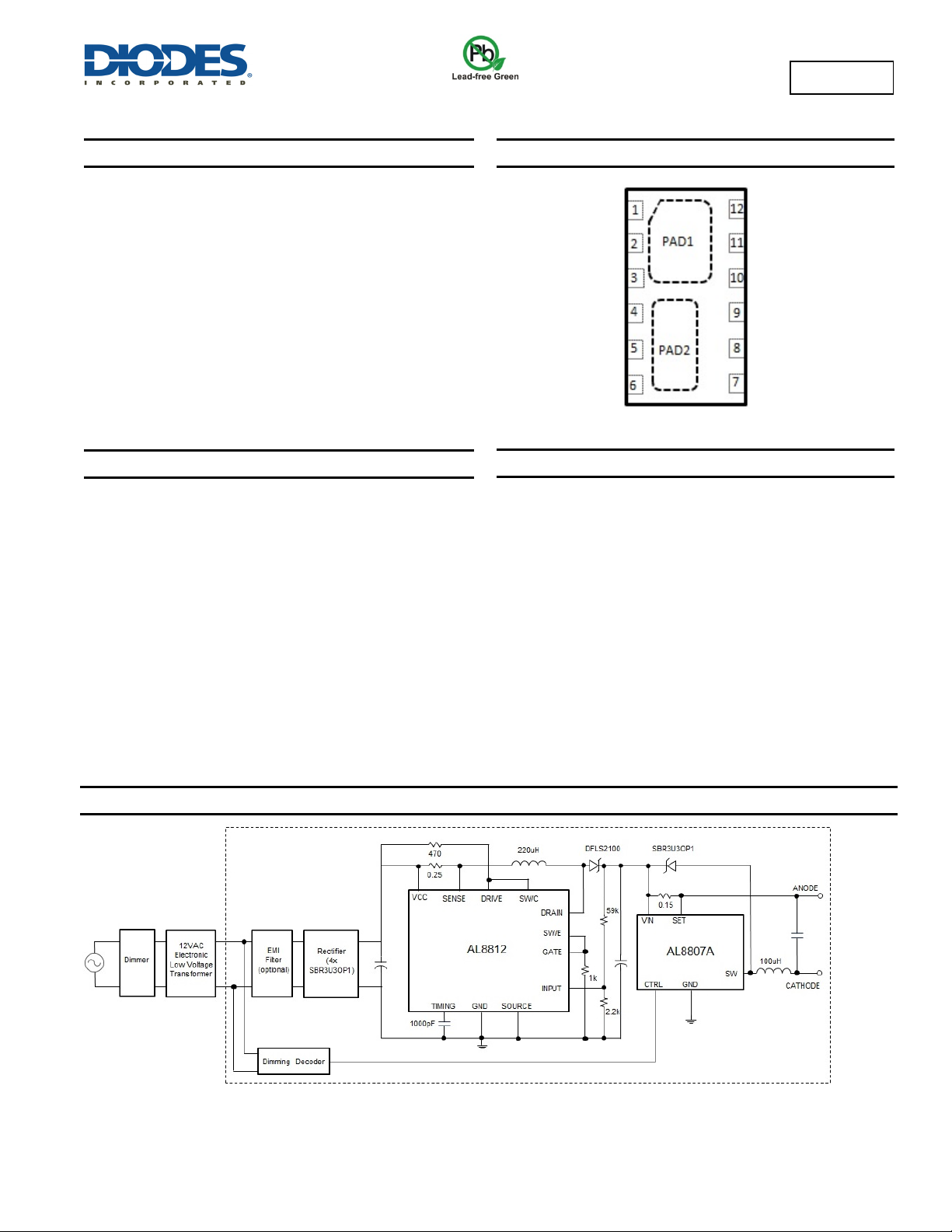
Pin Assignments
The AL8812 is a monolithic control circuit containing the primary
functions required for DC-to-DC converters with MOSFET in one
package. These devices consist of an internal temperature
compensated reference, comparator, controlled duty cycle oscillator
with an active current limit circuit, driver and high current output
switch. Additionally a 60V, 3.6A MOSFET is integrated for reduced
BOM cost and size. This series is specifically designed for buck and
boost applications with a minimum number of external components.
Features
• Operation from 3.0V to 20V Input
• Integrated 60V, 3.6A MOSFET
• Low Standby Current
• Current Limiting
• Output Voltage Adjustable
• Frequency Operation to 100 kHz
• Precision 2% Reference
• Totally Lead-Free & Fully RoHS Compliant (Notes 1 & 2)
• Halogen and Antimony Free. “Green” Device (Note 3)
Notes: 1. No purposely added lead. Fully EU Directive 2002/95/EC (RoHS) & 2011/65/EU (RoHS 2) compliant.
2. See http://www.diodes.com/quality/lead_free.html for more information about Diodes Incorporated’s definitions of Halogen- and Antimony-free, "Green"
and Lead-free.
3. Halogen- and Antimony-free "Green” products are defined as those which contain <900ppm bromine, <900ppm chlorine (<1500ppm total Br + Cl) and
<1000ppm antimony compounds.
NC
GATE
INPUT
1
2
3
4
VCC
SENSE
DRIVE
5
6
U-DFN6040-12
Applications
• Low Voltage LED Lighting such as MR-16
• General Purpose DC-DC Converter
12
11
10
9
8
7
DRAIN
SOURCE
TIMING
GND
SW/E
SW/C
Typical Applications Circuit
(For detailed schematic please contact your Diodes Sales Representative)
AL8812
Document number: DS37099 Rev. 1 - 2
Dimmable MR-16 LED Driver System Diagram
1 of 11
www.diodes.com
March 2014
© Diodes Incorporated
Page 2
A
r
r
r
_
Pin Descriptions
L8812
Pin
Name
NC 1 No Connection
GATE 2 Gate connection of internal MOSFET.
INPUT 3 Feedback pin for inverting input of internal comparator
VCC 4 Supply voltage pin
SENSE 5 No Connection.
DRIVE 6
SW/C 7 Internal switch transistor collector
SW/E 8 Internal switch transistor emitter
GND 9 Ground Connection
TIMING 10 Timing Capacitor to control the switching frequency.
SOURCE 11 Source connecton of internal MOSFET
DRAIN 12 Drain connection of internal MOSFET
Exposed PAD1 Exposed Pad of MOSFET Drain
Exposed PAD2 Exposed Pad of AL8812 and connect to PCB ground
Pin
Number
(U-DFN6040-12)
Current drive collector:
Normally connected to V
Function
directly or via a resistor.
CC
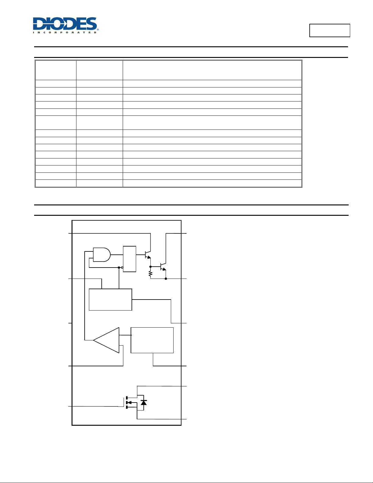
Functional Diagram
D RIVE
6
7
SW/C
SENSE
VCC
INPUT
GATE
5
4
AL8812
Document number: DS37099 Rev. 1 - 2
S
Q
R
Ipk
Oscillato
3
2
C
Comparato
+
T
100
1.25V
Reference
Regulato
Q2
Q1
8
10
9
12
11
www.diodes.com
SW/ E
TIMING
GND
DRAIN
SOURCE
2 of 11
March 2014
© Diodes Incorporated
Page 3
A
Absolute Maximum Ratings (@T
= +25°C, unless otherwise specified.)
A
Symbol Parameter Value Unit
VCC
VIR
Power Supply Voltage 20 V
Comparator Input Voltage Range -0.3 to +36 V
SW/C Switch Collector Voltage 36 V
SW/E
V
CE (switch)
Switch Emitter Voltage (V
Switch Collector to Emitter Voltage 36 V
1 = 40V)
Pin
36 V
DRIVE Driver Collector Voltage 36 V
I
C (driver)
ISW
VDS
VGS
I
SOURCE
PD
θJA
θJC
TMJ
TOP
T
stg
Driver Collector Current (Note 4) 100 mA
Switch Current 1.6 A
Maximum MOSFET Drain-Source voltage 60 V
Maximum MOSFET Gate-Source voltage +/-20 V
Maximum Continuous Source (Body Diode) Current 3.7 A
Continuous Power Dissipation (TA = +25°C)
(U-DFN6040-12 (derate 10mW/°C above +25°C)
1000 mW
Junction-to-Ambient Thermal Resistance 47.31
Junction-to-Case Thermal Resistance 6.42
Maximum Junction Temperature +150
Operating Junction Temperature Range
0 to +105
Storage Temperature Range -65 to +150
ESD HBM Human Body Model ESD Protection 250 V
ESD MM Machine Model ESD Protection 100 V
Note: 4. Maximum package power dissipation limits must be observed.
Electrical Characteristics (@T
= +25°C, unless otherwise specified.)
A
Symbol Characteristics Min Typ Max Unit
OSCILLATOR
f
Frequency (V
osc
I
Charge Current (VCC = 5.0V to 40V, TA = +25°C)
chg
I
Discharge Current (VCC = 5.0V to 40V, TA = +25°C)
dischg
I
/ I
dischg
V
ipk (sense)
Discharge to Charge Current Ratio (Pin 7 to VCC, TA = +25°C)
chg
Current Limit Sense Voltage (I
5 = 0V, CT = 1.0nF, TA = +25°C)
PIN
= I
chg
, TA = +25°C)
dischg
24 33 42 kHz
24 30 42 μA
140 200 260 μA
5.2 6.5 7.5 —
300 400 450 mV
OUTPUT SWITCH (Note 5)
V
CE (sat)
V
CE (sat)
Saturation Voltage, Darlington Connection
(ISW = 1.0A, Pins 1,8 connected)
Saturation Voltage, Darlington Connection
(ISW = 1.0A, ID = 50mA, Forced ß ≈ 20)
hFE DC Current Gain (ISW = 1.0A, VCE = 5.0V, TA = +25°C)
I
Collector Off-State Current (VCE = 40V)
C (off)
— 1.0 1.3 V
— 0.45 0.7 V
50 75 — —
- 0.01 100 μA
OUTPUT MOSFET
V
GS(th)
VFD
R
DS(ON)
MOSFET Gate Threshold voltage 1 — 2.2 V
MOSFET Diodes forward voltage — .85 .95 V
Drain-source on-resistance (VGS = 10V, ID = 2.5A)
Drain-source on-resistance (VGS = 4.5V, ID = 2A)
— —
120
180
COMPARATOR
Vth
— 1.225 1.25 1.275 —
— 1.21 — 1.29 —
Reg
line
Threshold Voltage
TA = +25°C
TA = 0oC to +70oC
Threshold Voltage Line Regulation (VCC = 3.0V to 40V)
— — — V
— 1.4 6.0 mV
TOTAL DEVICE
ICC
Note: 5. Low duty cycle pulse techniques are used during test to maintain junction temperature as close to ambient temperature as possible.
Supply Current (VCC = 5.0V to 40V, CT =1.0nF, Pin 7 = VCC, V
= Gnd, remaining pins open)
> Vth Pin 2
Pin 5
— — 3.5 mA
AL8812
Document number: DS37099 Rev. 1 - 2
3 of 11
www.diodes.com
© Diodes Incorporated
L8812
°C/W
°C/W
°C
°C
°C
mΩ
mΩ
March 2014
Page 4
A
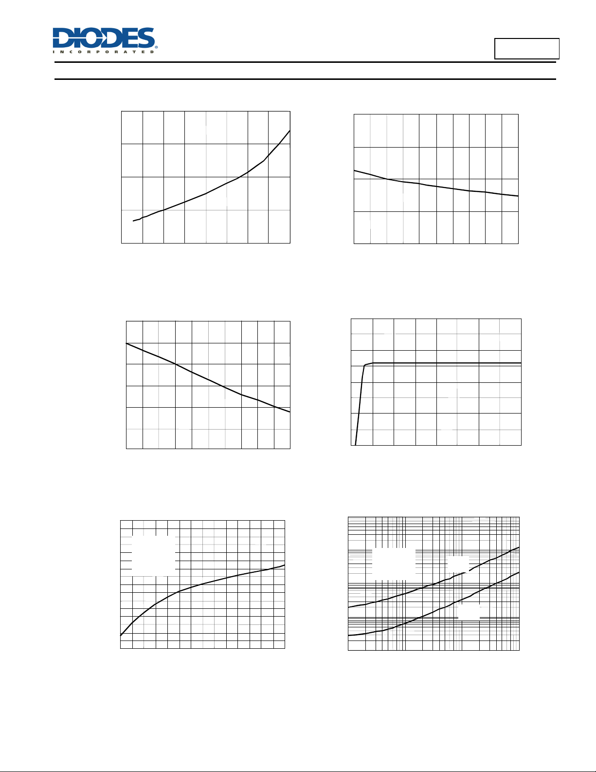
Performance Characteristics
Figure 1. Vce(sat) versus le
1.4
L8812
Figure 2. Reference Voltage versus Temp.
1.26
1.2
1
0.8
Vce(sat), Saturation Voltage (V)
0.6
0 0.2 0.4 0.6 0.8 1 1.2 1.4 1.6
Ie, Emitter Current (A)
Figure 3. Current Limit Sense Voltage
versus Temperature
440
420
400
380
360
Current Sense Voltage (mV)
340
320
0 1020 3040 50 6070 8090100
Temperature (oC)
1.255
1.25
Reference Voltage (V)
1.245
1.24
0 102030405060708090100
Temperature (oC)
Figure 4. Standby Supply Current
versus Supply Voltage
4.0
3.5
3.0
2.5
2.0
1.5
1.0
Icc, Supply Current (mA)
0.5
0.0
0 5 10 15 20 25 30 35 40
Vcc, Supply Voltage (V)
Figure 5. Emitter Follower Configuration
Output Saturation Voltage vs. Emitter Current
1.8
1.75
1.65
( sat), (V)
CE
V
1.55
1.45
Vcc=2~10V
Pin1,7,8=Vcc
Pin3,5=GND
1.7
T
=25oC
A
≤10W
Pin2=5
1.6
1.5
1.4
100 300 500 700 900 1100 1300 1500
AL8812
Document number: DS37099 Rev. 1 - 2
I
E
(mA)
1000
100
, Output Switch On-Off Time(us)
on-off
t
4 of 11
www.diodes.com
Figure 6.Output Switch On-Off Time versus
Oscillator Timing Capacitor
V
= 5.0V
CC
Pin 7 = V
CC
Pin 5 = GND
T
= 25oC
A
10
1
0.1
0.01 0.1 1 10
CT, Oscillator Timing Capacitor (
t
on
t
off
nF)
© Diodes Incorporated
March 2014
Page 5

A
L8812
T = 25°C
10
1
0.1
Drain Current (A)
D
I
0. 1 1 10
VDS Drain-Source Voltage (V)
10V 5V
4V
3.5V
3V
V
GS
2.5V
Output Characteristics
10
VDS = 10V
T = 150°C
1
T = 25°C
Drain Current (A)
0.1
D
I
23 45
VGS G a te -So urce V o ltage (V)
Typical Transfer Characte ristics
T = 150°C
10
1
0.1
Drain Current (A)
D
I
0.1 1 10
VDS Dr ain-So urc e V oltag e ( V)
10V
5V
Output Characteristics
1.8
GS(th)
1.6
1.4
and V
1.2
DS (on )
1.0
0.8
0.6
0.4
-50 0 50 100 150
Normali sed R
Tj Junction Temperature (°C)
VGS = 10V
ID = 2.5A
VGS = V
DS
ID = 250uA
R
V
Normalised Curves v Temperature
DS(on)
GS( th)
4V
3.5V
3V
2.5V
V
GS
2V
1
3V
0.1
T = 25°C
Drain-Source On-Resistance (W)
On-Resistance v Drain Current
DS( o n)
R
3.5V
110
ID Dr ain Cu rre nt (A )
4V
50 0
40 0
30 0
20 0
C
ISS
C
OSS
C
RSS
10 0
C Capacitance (pF)
0
110
VDS - Drain - Source Voltage (V)
4.5V
V
GS
5V
10V
VGS = 0V
f = 1MHz
10
1
T = 150°C
T = 25°C
0.1
Reve r se Dr ai n Cu rr ent (A )
I
0.4 0.6 0.8 1.0 1.2
SD
VSD Source-Drain Voltage (V)
Source-Drain Diode Forward Voltage
10
ID = 2 .5A
8
6
4
2
Gate-Source Voltage (V)
0
0123456
GS
V
Q - Charge (nC)
VDS = 30V
AL8812
Document number: DS37099 Rev. 1 - 2
Gate-Source Voltage v Gate ChargeCapacitance v Drain-Source Voltage
5 of 11
www.diodes.com
March 2014
© Diodes Incorporated
Page 6

A
L8812
Typical Application Circuits
Circuits shown below represent connections employed for different topologies. To use the integrated MOSFET the typical configuration below
can be used.
DRIVE
SW/C
SW/E
AL8812
AL8812
Document number: DS37099 Rev. 1 - 2
6 of 11
www.diodes.com
GATE
DRAIN
SOURCE
March 2014
© Diodes Incorporated
Page 7

A
Typical Application Circuits (cont.)
Boost Converter
L8812
Test Conditions Results
Line Regulation
Load Regulation
Output Ripple
Efficiency
AL8812
Document number: DS37099 Rev. 1 - 2
Vin = 9V to 12V, IO = 200mA
Vin = 12V, IO = 50mA to 200mA
Vin = 12V, IO = 200mA 500mVPP
Vin = 12V, IO = 200mA
7 of 11
www.diodes.com
20mV = ±0.035%
15mV = ±0.035%
80%
March 2014
© Diodes Incorporated
Page 8

A
Typical Application Circuits (cont.)
Buck Converter
L8812
Test Conditions Results
Line Regulation
Load Regulation
Output Ripple
Efficiency
AL8812
Document number: DS37099 Rev. 1 - 2
Vin = 12V to 24V, IO = 500mA
Vin = 24V, IO = 50mA to 500mA
Vin = 24V, IO = 500mA 160mVPP
Vin = 24V, IO = 500mA
8 of 11
www.diodes.com
20mV = ±0.2%
5mV = ±0.05%
82%
March 2014
© Diodes Incorporated
Page 9

A
)
)
t
)
5
5
p
)
)
pk (
)
pk (
)
)
)
pk (
)
pk (
)
pk (
)
(pp)
(pp)
L8812
Design Formula Table
Calculation Boost Buck
V
+ VF -V
tON / t
( tON + t
off
)
off
OUT
V
- V
IN (min
1/f 1/f
tON + t
t
off
tON ( tON +t
CT
I
(switch) 2I
k
tON
t
t
OFF
OFF
4.0×10
(tON / t
OUT (max
Rsc 0.3 / I
L
(min)
CO
V
= Saturation voltage of the output switch.
sat
V
= Forward voltage drop of the output rectifier.
F
( V
9
IN (min
I
– V
sat
I
switch
I
V
The following power supply characteristics must be chosen:
- Nominal input voltage.
V
IN
- Desired output voltage, |V
V
OUT
I
- Desired output current.
OUT
- Minimum desired output switching frequency at the selected values of Vin and Io.
f
min
V
- Desired peak-to-peak output ripple voltage. In practice, the calculated capacitor value will need to be increased due to its
ripple(pp)
| = 1.25 (1+R2/R1)
OUT
equivalent series resistance and board layout. The ripple voltage should be kept to a low value since it will directly affect the line and
load regulation.
V
IN (min
V
sa
tON + t
OFF
+1
) - t
( tON +t
OFF
-
tON 4.0×10
+1) 2I
off
0.3 / I
switch
)
t
on (max)
I
OUT tON
8V
ripple
( V
tON
OFF
IN(min
IN(min
– V
switch
switch
+ vF
OUT
- V
SAT
OFF
) - t
OFF
-
OUT(max
switch
-V
SAT
( t
OFF
ripple
- V
OFF
tON
)
OUT
+ tON )
OUT
+1
ON (max)
AL8812
Document number: DS37099 Rev. 1 - 2
9 of 11
www.diodes.com
March 2014
© Diodes Incorporated
Page 10

A
Ordering Information
Tube 13” Tape and Reel
Part Number Package Code Packaging
AL8812FDF-13 FDF U-DFN6040-12 NA NA 3000/Tape & Reel -13
Quantity
Part Number
Suffix
Quantity
Marking Information
(1) U-DFN6040-12
L8812
Part Number
Suffix
Package Outline Dimensions (All dimensions in mm.)
Please see AP02002 at http://www.diodes.com/datasheets/ap02002.pdf for latest version.
A
E
E1
AL8812
Document number: DS37099 Rev. 1 - 2
D1
D
D2
Z
A1
e
E2
b
10 of 11
www.diodes.com
A3
Seating Plane
L
U-DFN6040-12
Dim Min Max Typ
A 0.55 0.65 0.60
A1 0 0.05 0.02
A3 - - 0.15
b 0.35 0.45 0.40
D 5.95 6.05 6.00
D1 1.95 2.15 2.05
D2 2.35 2.55 2.45
e - - 1.00
E 3.95 4.05 4.00
E1 2.10 2.30 2.20
E2 1.80 2.00 1.90
L 0.35 0.45 0.40
Z - - 0.30
All Dimensions in mm
March 2014
© Diodes Incorporated
Page 11

A
L8812
Suggested Pad Layout
Please see AP02001 at http://www.diodes.com/datasheets/ap02001.pdf for the latest version.
DIODES INCORPORATED MAKES NO WARRANTY OF ANY KIND, EXPRESS OR IMPLIED, WITH REGARDS TO THIS DOCUMENT,
INCLUDING, BUT NOT LIMITED TO, THE IMPLIED WARRANTIES OF MERCHANTABILITY AND FITNESS FOR A PARTICULAR PURPOSE
(AND THEIR EQUIVALENTS UNDER THE LAWS OF ANY JURISDICTION).
Diodes Incorporated and its subsidiaries reserve the right to make modifications, enhancements, improvements, corrections or other changes
without further notice to this document and any product described herein. Diodes Incorporated does not assume any liability arising out of the
application or use of this document or any product described herein; neither does Diodes Incorporated convey any license under its patent or
trademark rights, nor the rights of others. Any Customer or user of this document or products described herein in such applications shall assume
all risks of such use and will agree to hold Diodes Incorporated and all the companies whose products are represented on Diodes Incorporated
website, harmless against all damages.
Diodes Incorporated does not warrant or accept any liability whatsoever in respect of any products purchased through unauthorized sales channel.
Should Customers purchase or use Diodes Incorporated products for any unintended or unauthorized application, Customers shall indemnify and
hold Diodes Incorporated and its representatives harmless against all claims, damages, expenses, and attorney fees arising out of, directly or
indirectly, any claim of personal injury or death associated with such unintended or unauthorized application.
Products described herein may be covered by one or more United States, international or foreign patents pending. Product names and markings
noted herein may also be covered by one or more United States, international or foreign trademarks.
This document is written in English but may be translated into multiple languages for reference. Only the English version of this document is the
final and determinative format released by Diodes Incorporated.
Diodes Incorporated products are specifically not authorized for use as critical components in life support devices or systems without the express
written approval of the Chief Executive Officer of Diodes Incorporated. As used herein:
A. Life support devices or systems are devices or systems which:
1. are intended to implant into the body, or
labeling can be reasonably expected to result in significant injury to the user.
B. A critical component is any component in a life support device or system whose failure to perform can be reasonably expected to cause the
failure of the life support device or to affect its safety or effectiveness.
Customers represent that they have all necessary expertise in the safety and regulatory ramifications of their life support devices or systems, and
acknowledge and agree that they are solely responsible for all legal, regulatory and safety-related requirements concerning their products and any
use of Diodes Incorporated products in such safety-critical, life support devices or systems, notwithstanding any devices- or systems-related
information or support that may be provided by Diodes Incorporated. Further, Customers must fully indemnify Diodes Incorporated and its
representatives against any damages arising out of the use of Diodes Incorporated products in such safety-critical, life support devices or systems.
Copyright © 2014, Diodes Incorporated
www.diodes.com
Y1
X1
Pin1
2. support or sustain life and whose failure to perform when properly used in accordance with instructions for use provided in the
AL8812
Document number: DS37099 Rev. 1 - 2
X3
C
X2
X
Y
G
Y3
Y2
G1
IMPORTANT NOTICE
LIFE SUPPORT
11 of 11
www.diodes.com
Dimensions
C 0.500
G 0.650
G1 0.350
X 0.250
X1 1.075
X2 1.275
X3 2.750
Y 0.400
Y1 1.150
Y2 1.000
Y3 2.300
Value
(in mm)
March 2014
© Diodes Incorporated
 Loading...