

Page 1
A
L8811
Boost/Buck/Inverting DC-DC CONVERTER
Description
The AL8811 is a monolithic control circuit containing the primary
functions required for DC-to-DC converters. These devices consist of
an internal temperature compensated reference, comparator,
controlled duty cycle oscillator with an active current limit circuit, driver
and high current output switch. This series is specifically designed for
incorporating in Boost, Buck and voltage-inverting applications with a
minimum number of external components.
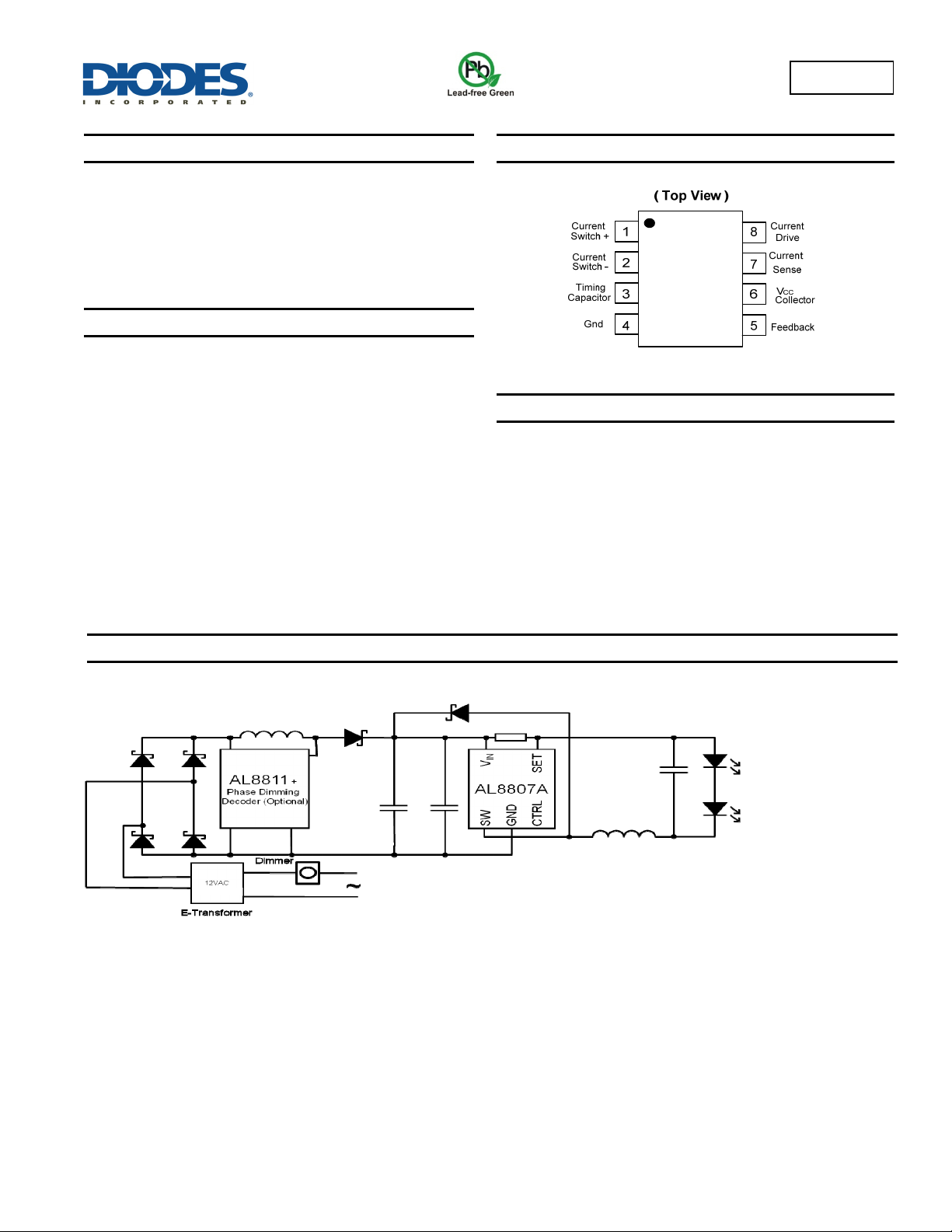
Pin Assignments
Features
Operation from 3.0V to 20V Input
Low Standby Current
Current Limiting
Output Switch Current to 1.6A
Output Voltage Adjustable
Frequency Operation to 100 kHz
Precision 2% Reference
Totally Lead-Free & Fully RoHS Compliant (Notes 1 & 2)
Halogen and Antimony Free. “Green” Device (Note 3)
Notes: 1. No purposely added lead. Fully EU Directive 2002/95/EC (RoHS) & 2011/65/EU (RoHS 2) compliant.
2. See http://www.diodes.com/quality/lead_free.html for more information about Diodes Incorporated’s definitions of Halogen- and Antimony-free, "Green"
and Lead-free.
3. Halogen- and Antimony-free "Green” products are defined as those which contain <900ppm bromine, <900ppm chlorine (<1500ppm total Br + Cl) and
<1000ppm antimony compounds.
Applications
Low Voltage LED Lighting such as MR-16
General Purpose DC-DC Converter
MSOP-8
Typical Application Diagram
Electronic Transformer compatible MR16 lamp Simplified Schematic
AL8811
Document number: DS36090 Rev. 2 - 2
1 of 11
www.diodes.com
June 2013
© Diodes Incorporated
Page 2
A
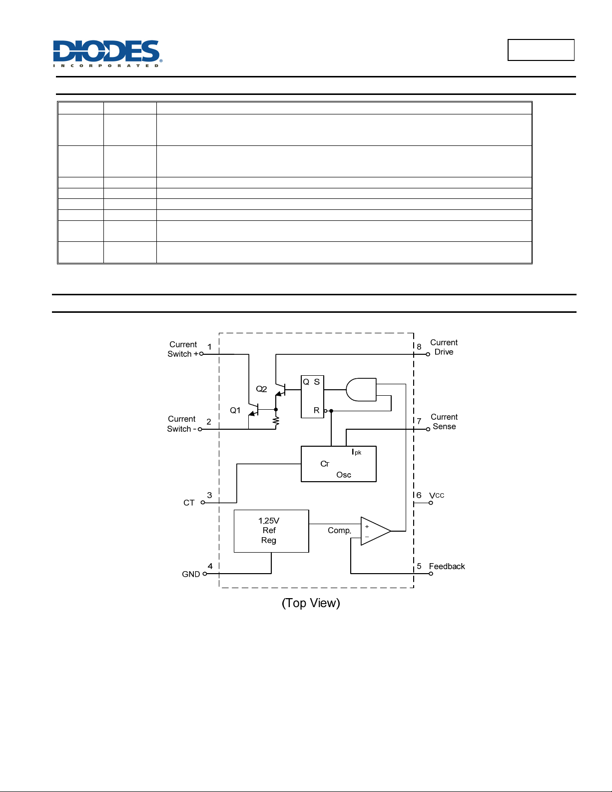
Pin Descriptions
Pin Name Pin Number Descriptions
Current
Switch+
Current
Switch-
CT 3 Timing Capacitor to control the switching frequency
GND 4
Feedback 5 Feedback pin for inverting input of internal comparator
VCC 6 Supply voltage pin
Current
Sense
Current
Drive
1
2
7
8
Internal switch transistor collector:
Connect to Inductor for boost converter.
Connect to VCC for Buck or Inverting converter
Internal switch transistor emitter:
Connect to GND for boost converter
Connect to Inductor for buck or inverting converter
Peak Current Sense Input by monitoring the voltage drop across an external current sense
resistor to limit the peak current through the switch
Current drive collector:
Normally connected to VCC directly or via a resistor.
L8811
Functional Diagram
AL8811
Document number: DS36090 Rev. 2 - 2
2 of 11
www.diodes.com
June 2013
© Diodes Incorporated
Page 3
A
L8811
Absolute Maximum Ratings (@T
= +25°C, unless otherwise specified.)
A
Symbol Parameter Rating Unit
VCC
VIR
V
C (SWITCH)
V
E (SWITCH)
V
CE (SWITCH)
V
C (DRIVER)
I
C (DRIVER)
ISW
PD
JA
TMJ
T
STG
Power Supply Voltage 20 V
Comparator Input Voltage Range -0.3 to +36 V
“Current Switch +” Collector Voltage 36 V
„Current Switch –„ Emitter Voltage (V
“Current Switch” Collector to Emitter Voltage 36 V
“Current Drive” Collector Voltage 36 V
1 = 36V)
PIN
36 V
“Current Drive” Collector Current 100 mA
“Current Switch” Current 1.6 A
Power Dissipation (Note 4) 600 mW
Thermal Resistance 130
Maximum Junction Temperature +150
Storage Temperature Range -65 to +150
C/W
C
C
ESD HBM Human Body Model ESD Protection 1 kV
ESD MM Machine Model ESD Protection 150 V
Caution: Stresses greater than the 'Absolute Maximum Ratings' specified above, may cause permanent damage to the device. These are stress ratings only;
Semiconductor devices are ESD sensitive and may be damaged by exposure to ESD events. Suitable ESD precautions should be taken when handling
functional operation of the device at these or any other conditions exceeding those indicated in this specification is not implied. Device reliability may be
affected by exposure to absolute maximum rating conditions for extended periods of time.
and transporting these devices.
Recommended Operating Conditions
Symbol Parameter Min
Max
Unit
VCC Supply Voltage 3 20 V
TOP
Operating Junction Temperature Range
-40
Electrical Characteristics (@ V
= 5V, TA = +25°C, unless otherwise specified.)
CC
Symbol Parameter Min Typ Max Unit
OSCILLATOR
f
OSC
I
CHG
I
DISCHG
I
DISCHG
V
IPK (SENSE)
Frequency (V
5 = 0V, CT = 1.0nF, TA = +25°C)
PIN
Charge Current (VCC = 5.0V to 20V, TA = +25°C)
Discharge Current (VCC = 5.0V to 20V, TA = +25°C)
/ I
Discharge to Charge Current Ratio (Pin 7 to VCC, TA = +25°C)
CHG
Current Limit Sense Voltage (I
CHG
= I
DISCHG
, TA = +25°C)
24 33 42 kHz
24 30 42 µA
140 200 260 µA
5.2 6.5 7.5 —
300 400 450 mV
OUTPUT SWITCH (Note 4)
V
CE(sat)
V
CE(sat)
Saturation Voltage, Darlington Connection
(I
= 1.0A, Pins 1, 8 connected)
SW
Saturation Voltage, Darlington Connection
(I
= 1.0A, ID = 50mA, Forced ß 20)
SW
hFE DC Current Gain (ISW = 1.0A, VCE = 5.0V, TA = +25°C)
I
Collector Off-State Current (VCE = 20V)
C(off)
— 1.0 1.3 V
— 0.45 0.7 V
50 75 — —
— 0.01 100 µA
COMPARATOR
Vth Threshold Voltage TA = +25°C
Reg
Threshold Voltage Line Regulation (VCC = 3.0V to 20V)
(LINE)
1.225 1.25 1.275 V
— 1.4 6.0 mV
TOTAL DEVICE
ICC
Supply Current (V
> Vth Pin 2 = Gnd, remaining pins open)
V
PIN 5
= 5.0V to 20V, CT =1.0nF, Pin 7 = VCC,
CC
— 3.5 mA
—
AL8811
Document number: DS36090 Rev. 2 - 2
3 of 11
www.diodes.com
+105
C
June 2013
© Diodes Incorporated
Page 4
A
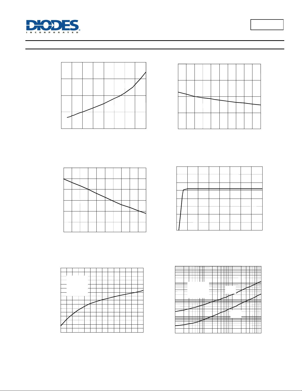
Typical Performance Characteristics
Figure 1. Vce(sat) versus le
1.4
L8811
Figure 2. Reference Voltage versus Temp.
1.26
1.2
1
0.8
Vce(sat), Saturation Voltage (V)
0.6
0 0.2 0.4 0.6 0.8 1 1.2 1.4 1.6
Ie, Emitter Current (A)
Figure 3. Current Limit Sense Voltage
versus Temperature
440
420
400
380
360
Current Sense Voltage (mV)
340
320
0 102030 40 50 6070 8090100
Temperature (oC)
1.255
1.25
Reference Voltage (V)
1.245
1.24
0 102030405060708090100
Temperature (oC)
Figure 4. Standby Supply Current
versus Supply Voltage
4.0
3.5
3.0
2.5
2.0
1.5
1.0
Icc, Supply Current (mA)
0.5
0.0
0 5 10 15 20 25 30 35 40
Vcc, Supply Voltage (V)
Figure 5. Emitter Follower Configuration
Output Saturation Voltage vs. Emitter Current
1.8
1.75
Vcc=2~10V
Pin1,7,8=Vcc
Pin3,5=GND
1.7
T
=25oC
A
10W
Pin2=5
1.65
( sat), (V)
1.6
CE
V
1.55
1.5
1.45
1.4
100 300 500 700 900 1100 1300 1500
AL8811
Document number: DS36090 Rev. 2 - 2
I
E
(mA)
1000
100
10
, Output Switch On-Off Time(us)
on-off
t
0.1
4 of 11
www.diodes.com
Figure 6.Output Switch On-Off Time versus
Oscillator Timing Capacitor
V
= 5.0V
CC
Pin 7 = V
CC
Pin 5 = GND
T
= 25oC
A
1
0.01 0.1 1 10
CT, Oscillator Timing Capacitor (
t
on
t
off
nF)
© Diodes Incorporated
June 2013
Page 5

A
Application Circuit
(1) Boost Converter
Test Conditions Results
Line Regulation
Load Regulation
Output Ripple
Efficiency
V
= 9V to 12V, IO = 200mA
IN
V
= 12V, IO = 50mA to 200mA
IN
V
= 12V, IO = 200mA 500mVPP
IN
V
= 12V, IO = 200mA
IN
20mV = ±0.035%
15mV = ±0.035%
80%
L8811
AL8811
Document number: DS36090 Rev. 2 - 2
5 of 11
www.diodes.com
June 2013
© Diodes Incorporated
Page 6

A
Application Circuit (cont.)
(2) Electronic Transformer compatible triac dimmable MR16/GU5.3 lamp for 120Vac
L8811
Circuit Description
This design consists of three sections:
1) The input PFC circuit converts the 12V
2) The output Buck LED Driver drives the three LEDs in series at a fixed current (AL8807A).
3) Finally, the phase-detect circuit generates a voltage proportional to the phase of the incoming AC voltage (when triac dimming is used).
AC input voltage to a DC voltage around 30V (AL8811).
PFC Circuit
The AL8811 Boost converter is a simple “Constant ON time controller”. By keeping the same ON time throughout the AC cycle, the circuit will
draw a current that will closely match the voltage and result in a constant input current. This eliminates the classic peak current problem with a
bridge rectifier and a large input filter capacitor.
The PFC circuit includes the input bridge rectifier, EMI filter (if needed) and the AL8811 Boost converter. The AC input voltage is rectified by the
bridge circuit and filtered by C1, R1, C4, and C5. This first filter removes the high frequency that is generated by the Electronic Transformer in the
range of 20-30 KHz. An additional diode rectifier circuit (D5, C2) is used to generate a voltage that is used to power the circuit that will turn on/off
the external MOSFET of the Boost converter. This circuit is very important as the gate drive of the MOSFET has to be greater than 3-4 volts
throughout the AC cycle. The external MOSFET is used to reduce the heat dissipation in the AL8811.
The AL8811 has a current limit resistor R3 which sets the maximum current allowed through the inductor L1. The output voltage is set by the
divider R6, R5 to an output of around 35 volts. The output voltage is filtered by the two capacitors C8 and C9. These two capacitors store energy
that will be used when the input voltage is low during the AC cycle.
AL8811
Document number: DS36090 Rev. 2 - 2
6 of 11
www.diodes.com
June 2013
© Diodes Incorporated
Page 7

A
L8811
Application Circuit (cont.)
Buck LED Driver
The AL8807A is a step-down DC-DC converter designed to drive LEDs with a constant current. The current through the LED is controlled by R11.
In the present Evaluation board, the current is set to around 660mA based on a resistor value of 0.15Ω. The current is set using the “CTRL” input
pin which in this new version of the IC can vary from 0 to 2.5V, controlling the current from 0mA to the maximum current at 2.5V. This control input
pin is used to lower the LED current as the TRIAC dims the LED. In this way, the energy stored in the two output capacitors of the PFC circuit will
be able to provide current throughout the AC cycle.
TRIAC Phase Detection Circuit
The phase of the TRIAC is detected by using an additional rectifier circuit that generates a voltage in proportional to the phase of the TRIAC Driver.
This is done by rectifying the input AC voltage and averaging the energy using a resistor to charge a capacitor. Two additional resistors in series,
R12 and R8, slowly discharge this circuit so it will follow the input phase change. The two resistors, R12 and R8, are used to scale the voltage so
the range is from 0 to 2.6V to the Buck LED driver control pin.
A simple transistor emitter follower circuit is used to drive a 1KΩ resistor in the emitter circuit. This low resistance is needed to drive the input
control pin of the AL8807A LED driver because the pin outputs a small current of 50uA, which limits the lowest control voltage to around 50 mV.
Setting the LED output current (AL8807A):
The LED output current is set using resister R11 and the formula:
= V
I
LED
For a current of 660mA, R11 is about 0.15Ω
/ R11 where VTH is equal to 0.1V
TH
.
Setting the PFC Variables (AL8811)
The choice for the size of the boost converter inductor selected in this design is based on a compromise which it is able to support a peak current to
around 1.5A since the average input voltage will be around 12-14V.
The boost converter (AL8811) includes a current limit resistor R3 which will limit the current through the inductor and thus the power delivered to the
output load. The formula for the resistor is:
PK(switch)
= 0.33V / R3
7 of 11
www.diodes.com
June 2013
© Diodes Incorporated
I
For a current limit of 1A, R3 is 0.33Ω.
In this evaluation design, this value was selected based on having three LEDs in series drawing about 660mA. It was found that two 68µF
capacitors mounted in parallel would just fit into the cavity of the MR16 bulb. The important design goal is to have the PFC circuit, which is used to
always draw current from the Electronic Transformer.
AL8811
Document number: DS36090 Rev. 2 - 2
Page 8

A
Application Circuit (cont.)
(3) Buck Converter
Test Conditions Results
Line Regulation
Load Regulation
Output Ripple
Efficiency
V
= 12V to 20V, IO = 500mA
IN
= 20V, IO = 50mA to 500mA
V
IN
V
= 20V, IO = 500mA 160mVPP
IN
V
= 20V, IO = 500mA
IN
L8811
20mV = ±0.2%
5mV = ±0.05%
82%
1
SQ
R
CT
Comp.
Osc
I pk
+
_
R2
36k
1.0uH
Vout
+
100
Optional Filter
Vout
5.0V/500mA
CO
Q2
Q1
2
B240
3
L100uH
CT
1.25V
470
pF
4
+
470uF
Ref
Reg
8
7
Rsc
0.11
6
C
VC
+
5
Vin
20
470
uF
R125k
AL8811
Document number: DS36090 Rev. 2 - 2
8 of 11
www.diodes.com
June 2013
© Diodes Incorporated
Page 9

A
Application Circuit (cont.)
(4) Voltage Inverting Converter
Test Conditions Results
Line Regulation
Load Regulation
Output Ripple
Efficiency
V
= 4.5V to 6.0V, IO = 100mA
in
V
= 5.0V, IO = 20mA to 100mA
in
V
= 5.0V, IO = 100mA 500mVPP
in
V
= 5.0V, IO = 100mA
in
L8811
20mV = ±0.08%
30mV = ±0.12%
60%
AL8811
Document number: DS36090 Rev. 2 - 2
9 of 11
www.diodes.com
June 2013
© Diodes Incorporated
Page 10

A
Ordering Information
L8811
Part Number Package Code Packaging
AL8811M8-13 M8 MSOP-8 NA NA 2500/Tape & Reel -13
Quantity Part Number Suffix Quantity Part Number Suffix
Tube 13” Tape and Reel
Marking Information
(1) MSOP-8
( Top View )
87 65
Internal Code
Logo
Y W X
Y : Year : 0~9
W : Week : A~Z : 1~26 week;
Part Number
AL8811
a~z : 27~52 week; z represents
52 and 53 week
234
1
Package Outline Dimensions (All dimensions in mm.)
Please see AP02002 at http://www.diodes.com/datasheets/ap02002.pdf for latest version.
AL8811
Document number: DS36090 Rev. 2 - 2
y
A2
A1
D
4
x
1
0
°
0.25
E
x
1
b
e
Gauge Plane
Seating Plane
A3
A
4
x
1
Detail C
E3
E1
0
°
a
L
c
See Detail C
10 of 11
www.diodes.com
MSOP-8
Dim Min Max Typ
A - 1.10 A1 0.05 0.15 0.10
A2 0.75 0.95 0.86
A3 0.29 0.49 0.39
b 0.22 0.38 0.30
c 0.08 0.23 0.15
D 2.90 3.10 3.00
E 4.70 5.10 4.90
E1 2.90 3.10 3.00
E3 2.85 3.05 2.95
e - - 0.65
L 0.40 0.80 0.60
a 0° 8° 4°
x - - 0.750
y - - 0.750
All Dimensions in mm
June 2013
© Diodes Incorporated
Page 11

A
L8811
Suggested Pad Layout
Please see AP02001 at http://www.diodes.com/datasheets/ap02001.pdf for the latest version.
DIODES INCORPORATED MAKES NO WARRANTY OF ANY KIND, EXPRESS OR IMPLIED, WITH REGARDS TO THIS DOCUMENT,
INCLUDING, BUT NOT LIMITED TO, THE IMPLIED WARRANTIES OF MERCHANTABILITY AND FITNESS FOR A PARTICULAR PURPOSE
(AND THEIR EQUIVALENTS UNDER THE LAWS OF ANY JURISDICTION).
Diodes Incorporated and its subsidiaries reserve the right to make modifications, enhancements, improvements, corrections or other changes
without further notice to this document and any product described herein. Diodes Incorporated does not assume any liability arising out of the
application or use of this document or any product described herein; neither does Diodes Incorporated convey any license under its patent or
trademark rights, nor the rights of others. Any Customer or user of this document or products described herein in such applications shall assume
all risks of such use and will agree to hold Diodes Incorporated and all the companies whose products are represented on Diodes Incorporated
website, harmless against all damages.
Diodes Incorporated does not warrant or accept any liability whatsoever in respect of any products purchased through unauthorized sales channel.
Should Customers purchase or use Diodes Incorporated products for any unintended or unauthorized application, Customers shall indemnify and
hold Diodes Incorporated and its representatives harmless against all claims, damages, expenses, and attorney fees arising out of, directly or
indirectly, any claim of personal injury or death associated with such unintended or unauthorized application.
Products described herein may be covered by one or more United States, international or foreign patents pending. Product names and markings
noted herein may also be covered by one or more United States, international or foreign trademarks.
This document is written in English but may be translated into multiple languages for reference. Only the English version of this document is the
final and determinative format released by Diodes Incorporated.
Diodes Incorporated products are specifically not authorized for use as critical components in life support devices or systems without the express
written approval of the Chief Executive Officer of Diodes Incorporated. As used herein:
A. Life support devices or systems are devices or systems which:
1. are intended to implant into the body, or
2. support or sustain life and whose failure to perform when properly used in accordance with instructions for use provided in the
labeling can be reasonably expected to result in significant injury to the user.
B. A critical component is any component in a life support device or system whose failure to perform can be reasonably expected to cause the
failure of the life support device or to affect its safety or effectiveness.
Customers represent that they have all necessary expertise in the safety and regulatory ramifications of their life support devices or systems, and
acknowledge and agree that they are solely responsible for all legal, regulatory and safety-related requirements concerning their products and any
use of Diodes Incorporated products in such safety-critical, life support devices or systems, notwithstanding any devices- or systems-related
information or support that may be provided by Diodes Incorporated. Further, Customers must fully indemnify Diodes Incorporated and its
representatives against any damages arising out of the use of Diodes Incorporated products in such safety-critical, life support devices or systems.
Copyright © 2013, Diodes Incorporated
www.diodes.com
AL8811
Document number: DS36090 Rev. 2 - 2
Y1
X C
Y
IMPORTANT NOTICE
LIFE SUPPORT
www.diodes.com
11 of 11
Dimensions Value (in mm)
C 0.650
X 0.450
Y 1.350
Y1 5.300
June 2013
© Diodes Incorporated
 Loading...