

Page 1
A
L8808
COST EFFECTIVE LOW EMI 30V 1A BUCK LED DRIVER
Description
The AL8808 is a step-down DC/DC converter designed to drive LEDs
with a constant current. The device can drive up to 8 LEDs,
depending on the forward voltage of the LEDs, in series from a
voltage source of 6V to 30V. Series connection of the LEDs provides
identical LED currents resulting in uniform brightness and eliminating
the need for ballast resistors. The AL8808 switches at frequency up to
1MHz with controlled rise and fall times to reduce EMI. This allows
the use of small size external components, hence minimizing the PCB
area needed.
Maximum output current of AL8808 is set via an external resistor
connected between the V
by applying either an analog DC voltage or a PWM signal at the
CTRL input pin. An input voltage of 0.4V or lower at CTRL switches
off the output MOSFET simplifying PWM dimming.
NEW PRODUCT
and SET input pins. Dimming is achieved
IN
Applications
• MR16 Lamps
• General Illumination Lamps
Notes: 1. No purposely added lead. Fully EU Directive 2002/95/EC (RoHS) & 2011/65/EU (RoHS 2) compliant.
2. See http://www.diodes.com for more information about Diodes Incorporated’s definitions of Halogen and Antimony free, "Green" and Lead-Free.
3. Halogen and Antimony free "Green” products are defined as those which contain <900ppm bromine, <900ppm chlorine (<1500ppm total Br + Cl)
and <1000ppm antimony compounds.
Pin Assignments
(Top View)
1
SW
GND
CTRL
2
3
54V
TSOT25
Features
• LED Driving Current Up to 1A
• Better Than 5% Accuracy
• High Efficiency Up to 96%
• Fast Controlled Falling Edges 7ns
• Operating Input Voltage from 6V to 30V
• High Switching Frequency Up to 1MHz
• PWM/DC Input for Dimming Control
• Built-In Output Open-Circuit Protection
• Built-In Over-Temperature Protection
• TSOT25: Available in “Green” Molding Compound (No Br, Sb)
Totally Lead-Free & Fully RoHS Compliant (Notes 1 & 2)
Halogen and Antimony Free. “Green” Device (Note 3)
IN
SET
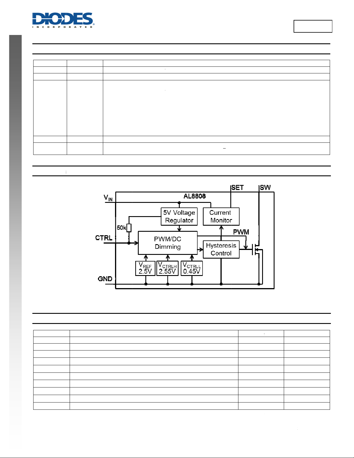
Typical Applications Circuit
AL8808
Document number: DS35648 Rev. 2 - 2
1 of 20
www.diodes.com
January 2013
© Diodes Incorporated
Page 2
r
i
a
M
e
n
o
a
a
M
e
g
e
u
t
p
a
p
e
n
e
a
e
C
d
f
V
o
m
m
e
a
e
m
e
o
a
w
r
a
e
0
l
l
b
P
c
e
a
t
o
g
o
a
u
T
p
h
e
h
k
p
c
o
s
o
i
n
d
e
n
e
r
2
d
i
t
h
R
e
o
s
2
g
0
5
0300
+
d
v
i
n
t
d
w
e
g
v
t
e
k
e
A
d
L8808
NEW PRODUCT
Pin Descr
Pin Number
1
2
3
4
5
Function
ptions
Pin Name
SW
GND
CTRL
SET
VIN
l Block Di
Switch Pin.
GND Pin
Dimming an
• Leave
(
• Drive t
• Drive w
I
OUTno
• Drive w
• A PWM
current
Set Nominal
Input Supply
section for
gram
onnect inducto
On/Off Control
loating for norm
= 5V, Giv
CTRL
voltage below
ith an analog vo
ith an analog vo
signal (low leve
to be adjusted
Output Current
Pin. Must be lo
ore information.
/freewheeling di
Input.
l operation.
s nominal avera
.4V to turn off o
tage (0.5V < V
tage > 2.6V out
l 0.4V and hig
elow the level s
in. Configure t
ally decoupled t
Function
de here, minim
ge output curre
tput current
< 2.5V) to a
C
RL
ut current will b
level > 2.6; tra
t by the resisto
e output current
o GND with > 2.
zing track lengt
t I
OUTnom
= 0.1/
just output curr
100% of I
OUTn
sition times les
connected to S
of the device.
µF X7R cerami
at this pin to re
)
S
nt from 20% to
m
than 1µs) allo
ET input pin.
c capacitor – se
uce EMI.
100% of
s the output
applications
Figure 1
.
AL8808 Bloc
Diagram
Absolute
aximum
Ratings
(@
T
A
= +25°C, unl
ss otherwise s
ecified.)
Symbol
ESD HBM
ESD MM
VIN
V
SET
VSW
V
CTRL
ISW
TJ
T
LEAD
T
ST
Caution: Stress
AL8808
Document numbe
s greater than th
functio
al operation of th
affecte
d by exposure to a
Semic
nductor devices
and tr
nsporting these d
: DS35648 Rev. 2
Human Body
Machine Mod
Continuous V
SET pin volta
SW voltage r
CTRL pin inp
Switch curren
Junction Tem
Lead Temper
Storage Tem
odel ESD Prot
l ESD Protectio
pin voltage rel
I
N
e relative to V
lative to GND
t voltage
erature
ture Soldering
erature Range
'Absolute Maxi
device at these
bsolute maximum
re ESD sensitive
vices.
- 2
Parameter
ction
n
tive to GND
pin
IN
um Ratings' spec
r any other condi
rating conditions f
nd may be dama
ified above, may
ions exceeding th
r extended period
ed by exposure t
2 of 20
ww.diodes.co
ause permanent
se indicated in th
of time.
ESD events. Sui
m
Ratin
2.5
20
-0.3 to
-5 to +
-0.3 to
-0.3 to
1.2
15
-55 to
amage to the de
s specification is
able ESD precaut
s
+33
0.3
+33
+6
150
ice. These are s
ot implied. Devic
ions should be ta
Unit
kV
V
V
V
V
V
A
°C
°C
°C
ess ratings only;
reliability may be
en when handling
January 201
© Diodes Incorporat
3
d
Page 3
A
Recommended Operating Conditions (@T
= +25°C, unless otherwise specified.)
A
Symbol Parameter Min Max Unit
VIN
V
CTRLH
V
CTRLDC
V
CTRLL
ISW
fSW
TJ
Note: 4. Subject to ambient temperature, input voltage and switching frequency. See applications section for suggested derating.
Electrical Characteristics (@ T
Symbol Parameter Conditions Min Typ Max Unit
V
NEW PRODUCT
INSU
V
INSH
IQ
IS
VTH
V
TH-H
I
SET
V
CTRL
R
CTRL
V
REF
R
DS(on)
I
SW_Lkg
tR
tF
T
OTP
T
OTP-Hyst
θJA
θJL
θJT
Notes: 5. Device mounted on FR-4 PCB (25mm x 25mm 1oz copper, minimum recommended pad layout on top layer and thermal vias to maximum area
bottom layer ground plane. For better thermal performance, larger copper pad for heat-sink is needed.
…Refer to Figure 42 for the device derating curve.
AL8808
Document number: DS35648 Rev. 2 - 2
Operating Input Voltage Relative to GND 6.0 30 V
Voltage High for PWM Dimming Relative to GND 2.6 5.5 V
Voltage Range for 20% to 100% DC Dimming Relative to GND 0.5 2.5 V
Voltage Low for PWM Dimming Relative to GND 0 0.4 V
Continuous Switch Current (Note 4) 1 A
Maximum Switching Frequency 1 MHz
Junction Temperature Range -40 +125 °C
= +25°C, VIN = 12V, CTRL pin floating; unless otherwise specified.)
A
Internal Regulator Start Up Voltage
Internal Regulator Hysteresis Threshold
Quiescent Current
Input Supply Current
VIN rising
VIN falling
VIN = 30V, output not switching
fSW = 250kHz
5.6 V
200 mV
350 µA
450 µA
Set Current Threshold Voltage 95 100 105 mV
Set Threshold Hysteresis ±20 mV
SET Pin Input Current
V
= V
IN
-0.1
SET
16 µA
Open Circuit CTRL Pin Voltage 5 V
CTRL Pin Input Resistance Referred to internal 5V regulator. 50 k
Internal Reference Voltage 2.5 V
On Resistance of SW MOSFET
Switch Leakage Current
SW Rise Time
SW Fall Time 5 ns
Over-Temperature Shutdown
Over-Temperature Hysteresis 10 °C
ISW = 0.35A
VIN = 30V, V
V
= 100 ±20mV, fSW = 250kHz
SENSE
CTRL
= 0.4V, V
SENSE
= 0V
VSW = 0.1V to 12V to 0.1V, CL = 15pF
0.35
0.5 µA
7 ns
145 °C
Thermal Resistance Junction-to-Ambient TSOT25 (Note 5) 209
Thermal Resistance Junction-to-Lead TSOT25 (Note 5) 57
Thermal Resistance Junction-to-Top TSOT25 (Note 5) 13
3 of 20
www.diodes.com
L8808
°C/W
January 2013
© Diodes Incorporated
Page 4
A
P
U
T
C
URRENT
F
REQ
UENCY
H
CUR
RENT
CTRL PIN CUR
REN
T
C
U
R
R
T ER
ROR
C
R
R
UTY CYC
Typical Performance Characteristics (@ T
NEW PRODUCT
400
350
300
(µA)
250
200
150
IN
100
50
0
0 3 6 9 12 15 18 21 24 27 30
INPUT VOLTAGE (V)
Figure 2. Supply Current vs. Input Voltage
1.2
R
T = +25°C
A
V= 12V
IN
1.0
L = 68µH
1 LED
0.8
(A)
SET
R
0.6
0.4
LED
0.2
V = 0V
CTRL
V = V
SET IN
T = +25°C
A
= 100m
= 150m
SET
R
= 300m
SET
L8808
= +25°C, unless otherwise stated.)
A
900
800
700
z)
600
(k
500
400
300
200
100
0
20
Ω
0
-20
(µA)
Ω
-40
-60
-80
Ω
-100
L = 33µH
L = 100µH
T = +25°C
A
V = 12V
IN
R = 150m
SET
1 LED
L = 68µH
Ω
0.0 0.5 1.0 1.5 2.0 2.5 3.0 3.5 4.0 4.5 5.0
V
(V)
= 150m
CTRL
CTRL
Ω
Figure 3. Switching Frequency vs. V
T = +25°C, V = 12V
AIN
L = 68µH, R
1 LED
SET
0.0
0.0 0.5 1.0 1.5 2.0 2.5 3.0 3.5 4.0 4.5 5.0
V
(V)
Figure 4. LED Current vs. V
CTRL
CTRL
6
T = +25°C, V = 12V
AIN
L = 68µH, R
1 LED, f = 500Hz
5
PWM
SET
= 150m
Ω
(%)
4
3
EN
2
LED
1
0
020406080100
PWM DUTY CYCLE (%)
Figure 6. I vs. PWM Duty Cycle
LED
0.9
LED
0.6
U
ENT (A)
0.3
0.0
-120
0.0 0.5 1.0 1.5 2.0 2.5 3.0 3.5 4.0 4.5 5.0
V
(V)
Figure 5. I vs. V
CTRL
CTRL CTRL
100
90
80
70
60
LE (%)
50
40
D
30
20
T = +25°C, R = 150m
A SET
10
L = 33µH, L = 68µH, L = 100µH
0
6 9 12 15 18 21 24 27 30
INPUT VOLTAGE V
Ω
(V)
CTRL
Figure 7. Duty Cycle vs. Input Voltage
AL8808
Document number: DS35648 Rev. 2 - 2
4 of 20
www.diodes.com
January 2013
© Diodes Incorporated
Page 5
r
e
OSFET R
0
040302010
0
5
0
5
0
5
0
5
0
5
0
e
S
2
W
e
a
5
T
T
S
w
t
C
w
u
r
M
OSFET R
=
V
°
p
r
8
O
a
e
A
L8808
NEW PRODUCT
Typical P
Ω
(m )
DS(ON)
SW M
0.5
0.4
0.4
Ω
0.3
rformanc
6
0
V = Open
CTRL
V = V = 1
SET IN
5
0
0
0
0
0
0
-40 -25 -10 5
Figure 8.
V = 12V
IN
V = V
SET IN
T = +25°C
A
CTRL = Floating
Charact
V
20 35
AMBI
ENT TEMPERA
SW R vs
50 6
DS(ON)
ristics
(con
80 95 110 1
URE (°C)
. Temperature
.) (@ TA = +25°
25
, unless other
400
350
300
Ω
(m )
250
DS(ON)
200
150
100
SW
V
CTRL
V =
50
SET
T = 25
A
0
69
ise stated.)
Open
IN
C
12 15 1
Fig
ure 9. SW R
DS(
V
IN
21 24
(V)
vs. Input Volt
N)
27 30
ge
0.3
DS(ON)
0.2
0.2
0.1
SW MOSFET R ( )
0.1
0.0
0.0
0200
S
Figure 10.
400 600
ITCH CURREN
SW R vs.
DS(ON)
800 1
(mA)
witch Current
000
Fig
re 11. SW Out
ut Fall Time
Figure 12.
AL8808
Document numbe
: DS35648 Rev. 2
teady State W
- 2
veforms
5 of 20
ww.diodes.co
m
Figu
e 13. SW Outp
ut Rise Time
© Diodes Incorporat
January 201
3
d
Page 6
A
C
C
Y
C
URREN
T
TCHING F
REQ
UENC
Y
H
CUR
RENT
U
T
Y CYC
CUR
R
T
L8808
Typical Performance Characteristics (L = 68µH, T
NEW PRODUCT
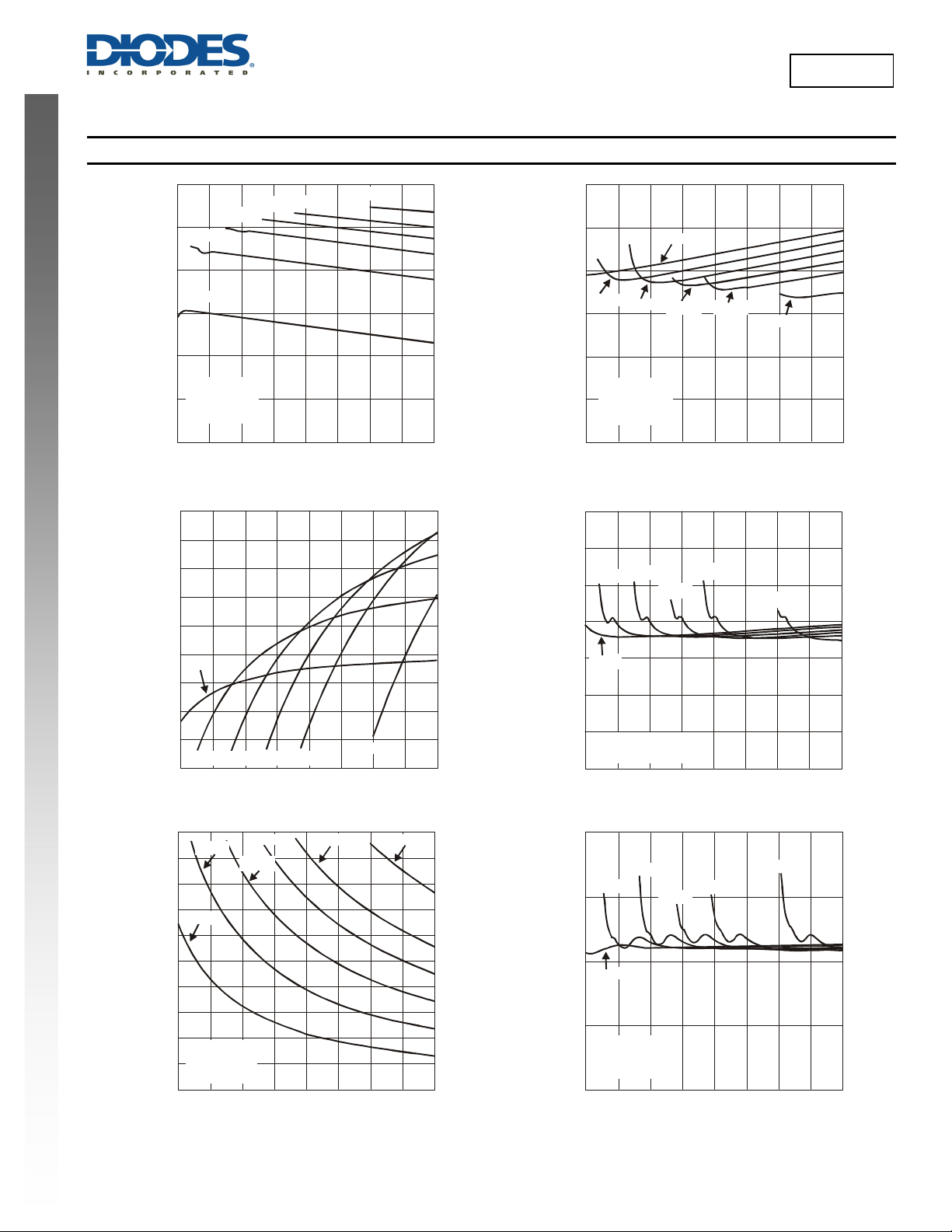
100
95
3 LEDs
2 LEDs
5 LEDs
4 LEDs
90
(%)
1 LED
85
IEN
80
EFFI
T = 25°C
A
L= 68µH
75
R = 150m
SET
Ω
70
6 9 12 15 18 21 24 27 30
INPUT VOLTAGE (V)
Figure 14. Efficiency vs. Input Voltage
450
400
z)
350
(k
300
250
7 LEDs
= +25°C, unless otherwise stated.)
A
0.36
0.35
0.34
(A)
2 LEDs
0.33
0.32
LED
0.31
0.30
6 9 12 15 18 21 24 27 30
Figure 15. 330mA LED Current vs. Input Voltage
0.74
0.72
2 LEDs
0.70
(A)
0.68
3 LEDs
T = 25°C
A
L= 68µH
R = 300m
SET
3 LEDs
1 LED
4 LEDs
Ω
5 LEDs
INPUT VOLTAGE (V)
5 LEDs
4 LEDs
7 LEDs
7 LEDs
200
150
1 LED
LED
0.66
0.64
1 LED
100
SWI
50
5 LEDs
3 LEDs
4 LEDs
2 LEDs
0
6 9 12 15 18 21 24 27 30
7 LEDs
INPUT VOLTAGE (V)
Figure 16. Switching Frequency vs. Input Voltage
100
90
2 LEDs
4 LEDs
3 LEDs
5 LEDs
80
70
1 LED
60
LE (%)
50
7 LEDs
0.62
T = 25°C, V
A
L= 68µH, R = 150m
0.60
6 9 12 15 18 21 24 27 30
SET
IN
= 12V
Ω
INPUT VOLTAGE (V)
Figure 17. 670mA LED Current vs. Input Voltage
1.10
7 LEDs
1.05
2 LEDs
3 LEDs
4 LEDs
5 LEDs
(A)
EN
1.00
1 LED
40
30
D
20
T = 25°C
A
L= 68µH
10
R = 150m
SET
0
6 9 12 15 18 21 24 27 30
Ω
INPUT VOLTAGE (V)
Figure 18. Duty Cycle vs. Input Voltage
LED
0.95
T = 25°C
A
L= 68µH
R = 100m
SET
0.90
6 9 12 15 18 21 24 27 30
Ω
INPUT VOLTAGE (V)
Figure 19. 1A LED Current vs. Input Voltage
AL8808
Document number: DS35648 Rev. 2 - 2
6 of 20
www.diodes.com
January 2013
© Diodes Incorporated
Page 7

A
T
O
R
OM TAR
GET
C
URR
T
TCHIN
G FREQ
U
NCY
H
TIO
R
OM TAR
GET
5
TCHIN
G FREQ
UENCY
H
O
N FR
O
R
G
5
TCHING FR
Q
U
C
Y
H
L8808
Typical Performance Characteristics (670mA LED Current; T
= +25°C unless otherwise stated.)
A
NEW PRODUCT
5
2 LEDs
(%)
EN
-1
3 LEDs
4 LEDs
3
1
1 LED
5 LEDs
7 LEDs
N F
I
-3
T = 25°C,
A
L = 33µH
DEVIA
-5
R = 150m
SET
Ω
186 9 12 15 21 24 27 30
INPUT VOLTAGE (V)
Figure 20. LED Current Deviation vs. Input Voltage
(%)
3 LEDs
2 LEDs
4
4 LEDs
3
5 LEDs
7 LEDs
2
1
0
1 LED
-1
N F
-2
-3
T = 25°C,
DEVIA
A
L = 68µH
-4
R = 150m
SET
Ω
-5
186 9 12 15 21 24 27 30
INPUT VOLTAGE (V)
Figure 22. LED Curr ent Deviation vs. Input Voltage
800
T = 25°C,
A
L = 33µH
z)
(k
E
700
600
500
R = 150m
SET
Ω
400
1 LED
300
200
SWI
100
0
2 LEDs
3 LEDs
4 LEDs
5 LEDs
186 9 12 15 21 24 27 30
7 LEDs
INPUT VOLTAGE (V)
Figure 21. Switching Frequency vs. Input Voltage
450
400
z)
350
(k
300
250
200
150
100
SWI
50
0
186 9 12 15 21 24 27 30
INPUT VOLTAGE (V)
Figure 23. Switching Frequency vs. Input Voltage
250
4
2 LEDs
3
ET (%)
2
1
M TA
0
1 LED
-1
3 LEDs
4 LEDs
7 LEDs
z)
(k
EN
E
200
150
100
5 LEDs
-2
-3
T = 25°C,
DEVIATI
A
L = 100µH
-4
-5
R = 150m
SET
Ω
186 9 12 15 21 24 27 30
INPUT VOLTAGE (V)
Figure 24. LED Current Deviation vs. Input Voltage
50
SWI
0
186 9 12 15 21 24 27 30
INPUT VOLTAGE (V)
Figure 25. Switching Frequency vs. Input Voltage
AL8808
Document number: DS35648 Rev. 2 - 2
7 of 20
www.diodes.com
January 2013
© Diodes Incorporated
Page 8

A
A
ON F
ROM
A
R
CUR
R
%
C
G F
REQ
C
Y
D
A
TIO
N FRO
M TAR
GET CUR
REN
T (%
TCHIN
G F
REQ
UENCY
H
5
D
TIO
N
F
R
O
M T
R
G
T
C
U
R
R
N
T
T
C
H
G
R
Q
U
C
Y
H
Typical Performance Characteristics (1A LED Current) T
5
)
NEW PRODUCT
2 LEDs
4
ENT (
3
2
1
GET
1 LED
0
T
-1
-2
-3
TI
T = 25°C
A
L = 33µH
-4
R = 100m
DEVI
SET
-5
Figure 26. LED Current Deviation vs. Input Voltage
4 LEDs
3 LEDs
Ω
5 LEDs 7 LEDs
18151269 30272421
INPUT VOLTAGE (V)
L8808
= +25°C unless otherwise stated.)
A
600
T = 25°C
A
L = 33µ H
500
R = 100m
SET
Ω
(kHz)
400
UEN
300
1 LED
200
HIN
100
SWIT
2 LEDs 3 LEDs 4 LEDs
0
5 LEDs
18151269 30272421
INPUT VOLTAGE (V)
Figure 27. Switching Frequency vs. Input Voltage
7 LEDs
5
)
4
2 LEDs
3
3 LEDs
4 LEDs
5 LEDs
7 LEDs
2
1
0
1 LED
-1
-2
-3
T = 25°C
A
L = 68µ H
-4
EVI
-5
R = 100m
SET
Ω
18151269 30272421
INPUT VOLTAGE (V)
Figure 28. LED Current Deviation vs. Input Voltage
(%)
E
E
A
4 LEDs
2 LEDs
4
3 LEDs
5 LEDs
3
2
1
0
1 LED
7 LEDs
-1
-2
-3
T = 25°C
A
L = 100µH
-4
EVIA
-5
R = 100m
SET
Ω
18151269 30272421
INPUT VOLTAGE (V)
Figure 30. LED Current Deviation vs. Input Voltage
300
z)
250
(k
200
150
100
50
SWI
0
18151269 30272421
INPUT VOLTAGE (V)
Figure 29. Switching Frequency vs. Input Voltage
200
180
z)
160
(k
140
EN
120
E
100
F
1 LED
80
IN
60
40
SWI
20
0
18151269 30272421
INPUT VOLTAGE (V)
Figure 31. Switching Frequency vs. Input Voltage
AL8808
Document number: DS35648 Rev. 2 - 2
8 of 20
www.diodes.com
January 2013
© Diodes Incorporated
Page 9

r
o
a
a
d
e
g
n
d
n
a
C
n
o
i
L
t
a
e
o
a
n
d
o
n
b
o
o
c
g
o
p
a
e
W
e
r
a
A
w
0
d
r
e
y
E
b
V
L
e
V
=
h
0
c
y
A
e
y
a
w
s
o
y
R
T
a
R
≈
b
s
h
g
r
t
E
e
a
o
a
o
e
m
o
n
t
8
5
t
e
u
i
w
o
e
5
i
f
e
A
n
a
p
s
n
o
s
L8808
NEW PRODUCT
Applicati
AL8808 Oper
In normal oper
inductor L1, an
voltage and the
This rising curr
voltage to the in
When this volta
L1, the LEDs a
of the LEDs an
This decaying c
applied at the i
This switch-on-
n Informa
tion
tion, when volt
the LEDs. Th
inductor L1.
nt produces a v
put of the intern
e reaches an i
d the schottky
the schottky di
urrent produces
put of the inter
nd-off cycle con
ion
ge is applied at
current ramps
ltage ramp acr
l comparator.
ternally set up
iode D1, and b
de.
a falling voltag
al comparator.
tinues to provid
+VIN, the AL88
up linearly, an
ss R1. The inte
er threshold, th
ck to the suppl
at R1, which is
hen this voltag
the average L
8 internal swit
the ramp rate
nal circuit of the
internal switch
rail, but it deca
sensed by the
e falls to the int
D current set b
h is turned on.
is determined
AL8808 sense
is turned off. T
s, with the rate
L8808. A volta
rnally set lowe
the sense resis
Current starts t
y the input volt
the voltage acr
e inductor curr
of decay deter
e proportional t
threshold, the i
or R1.
flow through s
ge (+VIN) min
ss R1 and appl
nt continues to
ined by the for
the sense volt
ternal switch is
nse resistor R1
s the LED chai
es a proportion
flow through R1
ard voltage dro
age across R1 i
turned on agai
,
l
,
.
LED Current
The LED curre
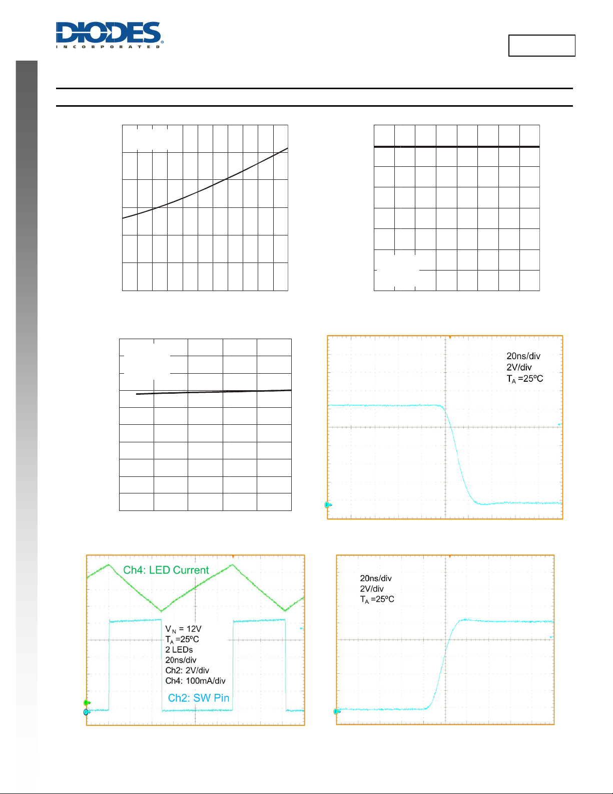
connected from
with CTRL left fl
If the CTRL pin
For example for
ontrol
t is controlled
the CTRL pin t
ating. If the CT
s driven by an e
a desired LED
y the resistor R
an internal 5V
RL pin is left flo
xternal voltage (
urrent of 660m
Figure 32.
(in Figure 32)
1
egulator. When
ting or driven a
higher than 0.5
and V
CTRL
R
When the CTR
AL8808
Document numbe
voltage is brou
: DS35648 Rev. 2
ht below 0.4V, t
- 2
he output switc
Where
I
Wher
=2.5
SET
Typical Applic
connected bet
the CTRL pin i
ove 2.5V the n
V
TH
=
I
LED
VTH is nominall
and lower than
ED
V
REF
or with the CT
V
TH
I
LED
is turned off wh
ww.diodes.co
V
CTRL
=
V
REF
is nomin
=
9 of 20
1R
1.0
66.0
tion Circuit
een VIN and S
left floating it g
minal average o
100mV.
2.5V), the aver
V
H
1
lly 2.5V
L pin left open
Ωm150
ich allows PWM
m
T pins. The AL
utput current in
ge LED current
the resulting res
dimming.
ts pulled up to
808 has an int
V - increasing
he LED(s) is de
is:
istor is:
rnal 50k resist
ts noise rejectio
ined as:
January 201
© Diodes Incorporat
r
n
3
d
Page 10

A
CUR
R
T
RAT
O
C
R
ROR
CUR
R
N
T
O
C
U
R
R
N
T
R
ROR
Application Information (cont.)
Analog Dimming
The CTRL pin can be driven by an external analog voltage (V
defined by R1. The LED current decreases linearly with the CTRL voltage when 0.5V V
Note that 100% brightness is achieved when either the CTRL pin is left floating or pulled above 2.5V by an external voltage source.
For 2.6V V
5.5V the LED current will not get overdriven and will be set the current according to the equation V
CTRL
reference voltage). See Figure 33 below.
110
T = 25°C
A
100
V = 12V
90
80
70
IN
L = 68µH
(%)
I
EN
60
NEW PRODUCT
50
40
30
20
10
DIMMED : 100% LED
0
0.0 0.5 1.0 1.5 2.0 2.5 3.0 3.5 4.0 4.5 5.0
Figure 33. LED Current Dimming Ration and
Typical Error vs. Control Voltage
PWM Dimming
LED current can be adjusted digitally, by applying a low frequency Pulse Width Modulated (PWM) logic signal to the CTRL pin to turn the device
on and off. This will produce an average output current proportional to the duty cycle of the control signal. In particular, a PWM signal with a
max resolution of 10bit (~0.1% duty cycle) can be applied to the CTRL pin to change the output current to a value below the nominal average
value set by resistor R
. To achieve this resolution the PWM frequency has to be lower than 500Hz, however higher dimming frequencies can
SET
be used, at the expense of dimming dynamic range and accuracy.
Typically, for a PWM frequency of 500Hz the accuracy is better than 2% for PWM ranging from 5% to 100%.
0.8
V = 12V
IN
T = +25°C
A
0.7
L = 68µH
(A)
0.6
0.5
R = 150m
SET
1 LED
Ω
E
0.4
0.3
LED
0.2
0.1
0
50 60010203040 9010070 80
PWM DUTY CYCLE (%)
Figure 34. PWM Dimming at 500Hz
), to adjust the output current to a value below the nominal average value
CTRL
2.5V.
CTRL
= 2.5V (the internal
CTRL
2.2
2.0
Dimmed LED Current Ratio
1.8
TYPI
1.6
1.4
AL E
1.2
1.0
(%)
0.8
0.6
LED Current Error
0.4
0.2
0.0
V (V)
CTRL
10
9
8
(%)
7
6
E
5
E
4
3
AD
L
2
1
10
Figure 35. Low Duty Cycle PWM Dimming at 500Hz
V = 12V
IN
T = +25°C
A
L = 68µH
R = 150m
SET
1 LED
Ω
7.50.0 2.5 5.0 15.010.0 12.5
PWM DUTY CYCLE (%)
L8808
AL8808
Document number: DS35648 Rev. 2 - 2
10 of 20
www.diodes.com
January 2013
© Diodes Incorporated
Page 11

r
o
n
s
W
e
e
e
d
a
t
e
o
M
e
o
H
H
e
e
e
e
P
e
m
w
g
s
.
e
r
c
c
c
y
s
w
u
W
e
g
d
t
w
t
u
r
n
a
t
e
e
e
u
m
u
A
e
e
A
A
g
s
g
s
d
o
s
s
Applicati
PWM Dimmi
The CTRL pin i
output stage.
The ultimate P
lower switching
the accuracy/lin
At the start of
threshold isn’t r
Greater PWM
frequency.
The three figure
from a 12V rail
n Informa
g
(cont.)
designed to b
M dimming res
frequencies and
arity of the PW
ach PWM cycl
ached then the
imming dynami
s below show 0.
t +25°C for a n
ion
(cont.)
driven by both
lution is determ
/or higher PWM
dimming.
the LED curr
accuracy will be
c ranges can b
2% duty cycle
minal LED curr
3.3V and 5V lo
ined by the num
frequencies the
nt needs to re
greatly affected
achieved by
WM pulse resol
nt of 670mA
.
ic levels directl
ber of full LED
number of full s
tart from zero
educing the P
ution with differ
from a logic ou
witching cycles
itching cycles
p to the uppe
M dimming fre
nt PWM freque
tput with either
hat can be achi
hat can be achi
threshold level
quency and/or i
cies and differe
n open drain o
ved during the
ved is reduced
(nominally 120
ncreasing the
nt inductor valu
L8808
tput or push pu
PWM on-time.
thereby reducin
mV/R
L8808 switchin
s driving 2 LED
SET
). If thi
ll
t
NEW PRODUCT
Figure 36. 0
.2% PWM Duty
68µ
Cycle at 100Hz
Inductance
PWM Frequen
y and
ure 37. 0.2% P
Fi
WM Duty Cycl
22µH Ind
at 100Hz PWM
ctance
Frequency an
Figure 38. 0
.2% PWM Duty
22µ
Cycle at 500Hz
Inductance
PWM Frequen
y and
As can be obse
value.
rved from Figur
37 greater di
ming accuracy
an be achieve
by reducing bo
th the PWM di
ming frequency
and the induct
r
AL8808
Document numbe
: DS35648 Rev. 2
- 2
11 of 20
ww.diodes.co
m
January 201
© Diodes Incorporat
3
d
Page 12

NEW PRODUCT
r
o
S
s
s
c
e
e
L
p
d
a
t
p
s
a
a
t
w
s
E
u
e
t
p
h
f
a
n
t
e
o
c
s
(
h
g
i
a
t
a
n
r
f
r
f
d
w
g
a
w
c
a
p
S
h
y
a
a
o
h
a
f
o
p
n
e
s
p
v
1
h
p
v
t
C
e
a
L
g
a
w
n
x
p
w
r
n
d
h
o
w
a
n
x
r
a
t
c
n
l
-
y
s
1
(
o
p
a
v
8
u
e
t
l
v
y
t
p
F
e
t
a
e
A
e
e
e
g
V
r
t
o
M
e
e
D
u
Applicati
Start-up and
On initial power
than 0.45V (typi
the output start
This will cause
the upper LED
The AL8808 do
accuracy.
Soft start can b
rail on the CTR
The external ca
occurs it is esse
This is achieve
the control volta
Adding this cap
dimming accura
n Informa
oft Start
up the device
cal). This cause
switching the L
ome additional i
urrent threshold
s not have in-b
easily implem
pin will charge
acitor slows up
ntial that the ca
by increasing t
ge at the input o
citor increases
cy depending o
ion
(cont.)
ill not start swit
a slight delay
D current will b
nput current to t
level by slowin
ilt soft-start act
nted by adding
he external cap
the ramp-up of
acitor is large e
e time taken fo
the comparato
the time taken
the delay intro
hing until the p
dependent on r
uild up to the up
I
LED
at of charging t
down the rise o
on allowing ver
n external cap
citor up to 5V.
the CTRL pin v
ough to keep t
the CTRL volt
.
or the output t
uced.
ower supply ha
mp rate of inpu
er threshold le
V
CTRL
=
SPK
e input bulk ca
f the CTRL pin
fast control of
citor from the
ltage thereby r
e CTRL pin volt
ge to rise to the
reach 90% of i
V5.2
reached appro
t voltage and in
el:
.0
×
2.1
1R
acitance. One
oltage – implem
he output Powe
TRL pin to grou
ducing the LED
ge below 2.5V
upper (turn-off)
ts final value, t
imately 5.6V o
ut bulk capacit
ay of reducing
enting a soft-sta
MOSFET swit
d. The internal
current via ana
uring the ramp
threshold and b
is delay is 25µ
the CTRL pin
nce of the AL8
his additional c
rt.
h which improv
pull-up resistor
og dimming. To
up of the input
slowing down
/nF, but will im
L8808
oltage is great
08 circuit). Onc
rrent is to reduc
s PWM dimmin
o the internal 5
ensure soft-sta
oltage.
he rate of rise
act on the PW
r
t
f
Figure
Reducing Ou
Peak to peak ri
A value of 1F
capacitor value
Note that the c
voltage. By add
altering the me
AL8808
Document numbe
put Ripple
ple current in th
will reduce the
.
pacitor will not
ing this capacit
n current value.
: DS35648 Rev. 2
39. Soft Start
LED(s) can be
supply ripple c
affect operatin
r the current w
- 2
ith 100nF Ca
reduced, if requ
urrent significa
frequency or
veform through
acitor on CTR
ired, by shuntin
tly in the typic
fficiency, but it
the LED(s) cha
12 of 20
ww.diodes.co
pin (VIN = 24V,
a capacitor C2
l case. Proporti
ill increase st
ges from a tria
m
I
= 667mA,
LED
across the LED
nally lower rip
rt-up delay, by
gular ramp to
LED)
s) as shown in
le can be achi
reducing the ra
more sinusoid
igure 32.
ved with high
e of rise of LE
l version witho
January 201
© Diodes Incorporat
r
t
3
d
Page 13

r
o
e
e
c
o
o
r
M
q
m
−
m
L
r
u
l
t
s
o
t
a
L
o
d
s
r
L
o
u
x
−
G
r
s
e
d
a
c
o
s
d
t
i
D
(
o
n
W
t
m
e
w
e
s
p
u
d
b
w
T
)
3
5
1
c
4
V
H
c
n
t
s
r
T
o
e
e
n
q
n
e
c
n
m
v
m
e
C
d
q
u
c
o
t
o
i
e
c
m
e
A
L8808
Applicati
Inductor Sel
Recommended
data for select
required switchi
LED current ac
n Informa
ction
inductor values
d component v
ng frequency.
uracy (due to pr
ion
(cont.)
for the AL8808
lues. The indu
ower inductor v
pagation delay
are in the rang
tance used will
alues can be u
) and increase
33µH to 100µ
depend on a
ed to increase t
ower dissipatio
. Note that th
ombination of I
he switching fre
(due to switchi
AL8808 Web
put voltage an
uency and red
g losses).
alculator provid
LED chain vo
ce solution siz
es performance
ltage to set the
but may affect
NEW PRODUCT
Figure 4
++
RrR
S
LS
rR
LS
0. Inductor Val
evice as possi
higher than the
n the table belo
CR
V)
093 2.
213 1.
124 1.
operating duty
with reference t
)
ernally set to 0.
inal}
d load current (
Part
=
V
IN
=
V
is the
uld be mounte
should have a
utput current.
use with the A
No.
TRF
ue should be ch
uations can be
e:
e:
D
ED
inductance (H)
resistance ()
rent sense resi
quired LED curr
pply voltage (V)
peak-peak rippl
otal LED forwar
witch resistance
de forward volt
: DS35648 Rev. 2
The inductor sh
The chosen coil
required mean
Suitable coils fo
MSS1038-333
MSS1038-683
NPIS64D330
The inductor val
The following e
Switch ‘On’ ti
t
ON
Switch ‘Off’ ti
t
OFF
Where:
L is the coil
is the coil
r
L
is the cu
R
S
I
is the re
avg
V
is the s
IN
I is the coi
V
LED
RSW is the
VD is the di
AL8808
Document numbe
L
−
IV
AVGLED
Δ
++
IV
AV
as close to the
aturation curren
8807 are listed
L
(µH)
33 0.
68 0.
33 0.
sen to maintai
sed as a guide,
Δ
I
(
IL
()
x
+
tance ()
nt (A)
e current (A) {In
voltage (V)
() {=0.35 no
ge at the requir
- 2
e with Input Vol
le with low resi
peak output cu
:
I
SA
(A
ycle and switch
o Figure 1 - Op
x I
AVG
)
13 of 20
ww.diodes.co
}
age and Numb
tance/stray indu
rent and a conti
Manufactu
ilCraft www.coi
C
NIC www.nicco
'on'/'off' times o
rating wavefor
m
r of LEDs
tance connecti
uous current ra
rer
lcraft.com
p.com
er the supply v
s.
Figur
41. Typical Sw
ns to the SW pi
ing above the
ltage and load
tching Wavefor
n.
urrent range.
January 201
© Diodes Incorporat
3
d
Page 14

A
Application Information (cont.)
Capacitor Selection
The small size of ceramic capacitors makes them ideal for AL8808 applications. X7R type is recommended because it retains capacitance value
over wider voltage and temperature ranges than other types such as Y5V or Z5U. X5R is a useful compromise over a restricted temperature
range. Note that even X7R capacitance reduces significantly with increased DC bias voltage. At 50% of rated voltage, the capacitance loss is
between about 10% to 50% of nominal. Therefore it is often necessary to select a voltage rating which is at least twice the operating voltage.
Input Capacitor
In Figure 32, the input capacitor C1 is required as a reservoir. Diode D1 switches at a rate of typically up to 400kHz. The power supply has a
finite impedance, often including a wiring inductance value of the order of 100nH to 1uH or more depending upon the system design. C1 is
required to limit the power supply voltage and current ripple both to allow stable regulation of the LED current, and also to meet EMC
requirements.
A 2.2F input capacitor is sufficient for most DC powered applications of AL8808. This depends upon the operating voltage and current and the
maximum level of ripple required. Additional capacitors may be required in parallel for EMC purposes. This is described below in a separate
section.
However, if operated from a rectified low voltage AC source, such as MR16, then the input capacitance will need to be significantly increased to
NEW PRODUCT
provide enough reservoir charge when the input voltage falls below the minimum operating voltage of the AL8808 or the LED chain voltage
Output Capacitor
In Figure 32, the output capacitor C2 is normally required to limit the load voltage and current ripple, in order to meet EMC requirements. A value
of 0.1µF to 1µF is sufficient for many requirements, depending on voltage and current conditions. Additional capacitors may be required in parallel
for EMC purposes. This is described below in a separate section.
Diode Selection
For maximum efficiency and performance, the flywheel rectifier (D1) should be a fast low capacitance Schottky diode with low reverse leakage at
the maximum operating voltage and temperature. The silicon PN diode is not suitable because of its increased power loss, due to a combination
of lower forward voltage and reduced recovery time. The use of a Super-Barrier-Rectifier (SBR) is not recommended for use as a flywheel diode
in this application. (However the SBR provides significant advantages when used with an AC power input as a bridge rectifier driving V
It is important to select D1 with a peak current rating above the peak coil current and a continuous current rating higher than the maximum output
load current. In particular, it is recommended to have a diode voltage rating at least 15% higher than V
safe operation during the switching and a mean current rating at least 10% higher than the peak diode current. The power rating is verified by
calculating the power loss through the diode. In practice, the voltage rating selection is often increased by up to about 50% to obtain a better
compromise with loss due to reverse leakage current at higher temperature. Also the current rating is typically selected to provide a margin of up
to about 50%.
Schottky diodes, e.g. DFLS240L or DFLS140, with their low forward voltage drop and fast reverse recovery, are the ideal choice for AL8808
applications. Leakage current is sufficiently limited for the application.
AL8808
Document number: DS35648 Rev. 2 - 2
14 of 20
www.diodes.com
to ensure
IN
© Diodes Incorporated
L8808
.)
IN
January 2013
Page 15

A
P
O
R
PATIO
Application Information (cont.)
Thermal Considerations
For continuous conduction mode of operation, the absolute maximum junction temperature must not be exceeded. The maximum power
dissipation depends on several factors: the thermal resistance of the IC package (
between junction and ambient temperature.
The maximum power dissipation can be calculated using the following formula:
TT
−
A)MAX(J
P
=
)MAX(D
θ
JA
where
T
T
is the maximum operating junction temperature; for the AL8808 this is +125°C.
J(MAX)
is the ambient temperature, and
A
is the junction to ambient thermal resistance.
JA
The major thermal path for the TSOT25 package is pin 2 (GND pin) and it is important for minimizing the
mass is associated with pin 2. The thermal impedance from the AL8808 junction to pin 2 is approximately 57°C/W.
The AL8808’s
NEW PRODUCT
area on bottom layer with 1oz copper standing in still air is approximately 209°C/W. Yielding a maximum power dissipation at 25°C of 0.47W
on a 25 x 25mm double sided FR4 PCB with minimum recommended pad layout on top layer and thermal vias to maximum
JA
The AL8808’s
on a 25 x 25mm double sided FR4 PCB with maximum area top and bottom with vias is approximately 151°C/W; which gives a
JA
maximum power dissipation at 25°C of 0. 66W.
Figure 42 shows the power derating of the AL8808 on different area PCB with maximum area on bottom of PCB with 1 and 2oz copper standing in
still air.
1.0
2
(50mm) with 2oz Cu max area top
0.9
0.8
0.7
N (W)
0.6
2
(50mm) with 1oz Cu max area top
2
(25mm) with 2oz Cu max area top
2
(25mm) with 1oz Cu min area top
2
(25mm) with 2oz Cu min area top
), PCB layout, airflow surrounding the IC, and difference
JC
that a suitable area and thermal
JA
L8808
0.5
2
DISSI
WE
0.4
(50mm) with 1oz Cu min area top
2
(25mm) with 1oz Cu min area top
0.3
0.2
0.1
0
-10 5-40 -25 50 6520 35 110 12580 95
AMBIENT TEMPERATURE (C)
Figure 42. Derating Curve for Different PCB
AL8808
Document number: DS35648 Rev. 2 - 2
15 of 20
www.diodes.com
January 2013
© Diodes Incorporated
Page 16

r
o
o
d
g
g
h
e
u
m
d
e
m
r
h
i
g
c
d
t
t
C
a
o
a
t
y
e
o
C
o
a
s
f
g
s
R
S
s
p
T
a
a
s
a
e
e
t
c
t
o
e
b
u
f
c
o
o
n
a
w
a
e
d
e
o
t
o
g
t
M
n
d
S
a
e
a
f
c
i
h
F
f
n
n
c
n
m
e
n
e
e
d
s
e
c
e
s
t
i
e
e
d
B
c
g
d
e
s
h
s
b
c
s
f
a
o
y
p
c
e
c
n
T
p
i
d
h
d
n
f
b
p
w
s
m
o
e
o
e
d
n
u
e
A
h
e
n
T
p
s
o
e
y
e
M
e
a
d
o
e
n
s
y
L8808
NEW PRODUCT
Applicati
EMI and Lay
The AL8808 is
decoupling and
switching spee
due to switchin
The turn-on ed
and PCB tracks
between the Sc
The tracks from
short as possibl
There is an ind
estimate the pri
and length will
The resonant fr
diode. An exa
n Informa
ut Considera
a switching reg
layout of the P
s of the internal
losses and radi
e (falling edge)
. After the Sch
ottky diode cap
the SW pin to
.
ctance internall
ary resonant fr
ominate the siz
quency of any
ple of good lay
ion
(cont.)
ions
ulator with fast
B.To help with
power MOSFE
ted EMI.
dominates the r
ttky diode rever
citance and th
he Anode of th
in the AL8808
equency. If the t
of the inductan
oscillation is de
ut is shown in Fi
edges and me
these effects th
. The rise an
diated EMI whi
e recovery time
track inductanc
Schottky diod
his can be assu
rack is capable
e.
ermined by the
gure 44 - the str
sures small dif
AL8808 has b
fall times are
ch is due to an
of around 5ns
e, L
, D1, and then
med to be arou
combined indu
ay track inducta
, See
TRACK
f handling 1A i
erential voltage
een developed
ontrolled to get
nteraction betw
as occurred; th
igure 43.
rom D1’s catho
d 1nH. For PC
creasing the thi
tance in the tra
ce should be le
; as a result o
o minimise radi
the right compr
en the Schottk
falling edge of
e to the decou
tracks a figure
kness will hav
ck and the effe
ss than 5nH.
this care has
ted emissions
mise between
diode (D1), S
the SW pin see
ling capacitors
of 0.5nH per m
a minor effect
tive capacitanc
to be taken wit
y controlling th
ower dissipatio
itching MOSFE
a resonant loo
C1 should be a
can be used t
n the inductanc
of the Schottk
Figure
PCB constructi
ound areas are
the g
(EMC
) operation and
capacitor C1 as
less t
an about 5mm.
the in
put current pas
tic inductance o
paras
more
round via hole
sense resistor
D1 anode, the
capacitor C2 a
itor and its cop
capa
impe
ance coupling d
: DS35648 Rev. 2
Figure 43. P
Summary:
1. Use a
2. Place
3. Place
4. Place
5. Place
AL8808
Document numbe
B Loop Reson
n with copper f
tightly connect
lso to minimize
close as possib
To ensure the
es directly thro
the copper tra
close to the gr
1 as close as p
W pin and the i
close as poss
er trace such th
ue to the added
- 2
ance
il on top and b
d together usin
device tempera
le to VIN, and as
est possible E
gh the capacito
e. Ensure low i
und pad.
ssible to VIN an
ductor as close
ible to L1 and
t the input curr
parasitic induct
ttom. Provide
plated via hol
ures by spreadi
close as possib
I filtering (great
r mounting pad.
ductance conn
SET.
together as pos
ET. To ensur
nt passes dire
nce of the copp
16 of 20
ww.diodes.co
aximum covera
s placed at reg
g the dissipate
le to the cathod
st attenuation),
This minimize
ction between t
ible to avoid rin
the best possi
tly through the
r trace.
m
44. Recomme
e of copper gro
ular intervals.
heat.
of D1. The se
place the capac
common impe
e capacitor an
ging.
le EMI filtering
apacitor mounti
ded PCB Layo
und plane on b
his is required
aration of these
tor and its copp
ance coupling
its ground con
(greatest atten
g pad. This mi
ut
th sides. Ensur
both for low E
nodes should b
r trace such th
ue to the adde
ection. Use 2
ation), place th
nimizes commo
January 201
© Diodes Incorporat
I
t
r
3
d
Page 17

A
Application Information (cont.)
EMI and Layout Considerations (cont.)
EMC Design
In addition to the layout instructions above, it may be necessary to take further measures to reduce electromagnetic interference (EMI) and meet
EMC requirements. This depends on the speed of the switching transitions. The fast switching edges include spectral harmonics spreading into
the UHF frequency range towards 500MHz. In this respect, AL8808 has been optimized to shape the switching current waveform to minimize EMI
while maintaining fast enough switching for high power efficiency. However, depending on the physical system design it may be necessary to add
additional filtering to reduce radiated and conducted emissions. The required circuit changes depend on a number of system design aspects
including the PCB size, the housing design and the length of external connecting wires.
Radiated Emission
Typically, the filtering required to control radiated emission consists of one or two additional capacitors placed close to the connecting points of the
wires. Very often the frequency range requiring most attenuation is in the region of 100MHz to 500MHz. In order to provide best attenuation in
this frequency range, use a capacitor of 1000pF to 2200pF with COG dielectric type, rated 50V or 100V. This capacitor provides very low ESR in
this frequency range. Place two such capacitors, one near the V
the best possible EMI filtering (greatest attenuation), place the capacitor and its copper trace such that the input or output current passes directly
NEW PRODUCT
through the capacitor mounting pad. This minimizes common impedance coupling due to the added parasitic inductance of the copper trace.
Conducted Emission
Conducted emission limits sometimes require filtering in the lower frequency range, from the switching frequency itself (Typically 200kHz) up to
about 30MHz. Usually the requirement only applies on the input side. The existing power supply may already include suitable measures. If
necessary add an input capacitor to reduce the ripple in this frequency range. Again the capacitors and their copper traces should be carefully
placed to avoid inductive common impedance coupling. Sometimes an additional series filter inductor may be added to achieve the desired
attenuation. An additional shunt capacitor to ground is connected resulting in a pi-filter configuration.
wire connection and one near the output connection to L1. Again, to ensure
IN
L8808
AL8808
Document number: DS35648 Rev. 2 - 2
17 of 20
www.diodes.com
January 2013
© Diodes Incorporated
Page 18

r
o
o
s
u
u
d
t
f
a
a
n
s
o
j
a
t
n
r
e
a
a
o
o
o
m
t
8
n
e
w
o
i
r
w
o
t
u
e
o
w
h
w
n
d
t
c
m
e
w
p
h
a
8
4
a
s
a
o
e
t
a
L
p
o
s
s
t
v
r
s
o
8
a
c
t
l
n
E
w
r
e
l
c
t
o
t
h
e
A
o
a
e
3
e
e
n
c
n
t
e
g
Applicati
Fault Conditi
The AL8808 ha
VIN and the SW
If the LEDs sho
the expected c
dramatically an
LEDs.
The on-time of
inductor. The of
32) causing a m
n Informa
n Operation
by default ope
pin will then fall
ld become sho
rrent - so no
the switching f
he internal pow
-time is signific
uch slower dec
ion
(cont.)
LED protectio
to GND. No exc
ted together the
xcessive heat
requency will m
er MOSFET sw
ntly increased b
y in inductor cu
. If the LEDs s
ssive voltages
AL8808 will co
ill be generate
st likely decrea
tch is significan
ecause the reve
rent.
ould become o
ill be seen by t
tinue to switch
within the AL
se. See Figure
ly reduced bec
rse voltage acro
en circuit the A
e AL8808.
nd the current t
808. However,
5 for an exam
use almost all
s the inductor i
8808 will stop
hrough the AL8
the duty cycle
le of this behav
f the input volt
now just the S
scillating; the S
08’s internal s
at which it ope
ior at 24V input
ge is now dev
hottky diode vo
L8808
T pin will rise t
itch will still be
ates will chang
voltage driving
loped across th
tage (See Figur
t
NEW PRODUCT
Figure 45. S
High Temper
The AL8808 is
temperature in
temperatures a
AL8808 off. Thi
The OTP shutd
never switch-off
unction temper
AL8808
Document numbe
ture Operati
high efficiency
excess of 100°
d hence juncti
will allow the ju
wn junction te
with a junction
ture of the AL8
: DS35648 Rev. 2
n and Protec
switching LED d
C given the c
n temperature
nction temperat
perature of th
emperature bel
08.
- 2
itching Chara
tion
river capable of
rrect thermal i
hen the Over-T
re of the AL880
AL8808 is app
w +125°C allo
teristics (norm
operating juncti
pedance to fr
mperature Pro
8 to cool down
roximately +145
ing the designe
18 of 20
ww.diodes.co
l open to shor
n temperatures
e air. If a fault
ection (OTP) of
nd potentially gi
°C with a hyste
r to design the
m
LED chain)
up to +125°C. T
should occur
the AL8808 wi
ing an opportu
esis of +10°C.
ystem thermally
his allows it ope
hat leads to in
l cut in turning
ity for the fault t
This means tha
to fully utilize t
rate with ambie
reased ambie
he output of th
clear itself.
the AL8808 wi
e wide operatin
January 201
© Diodes Incorporat
t
t
ll
3
d
Page 19

A
A
X
θ
Ordering Information
L8808XX
L8808
X-
PackingPackage
WT : TSOT25 7 : 7” Tape & Reel
Part Number Package Code Packaging
AL8808WT-7 WT TSOT25 3000/Tape & Reel -7
Marking Information
TSOT25
NEW PRODUCT
(Top View)
W
7
4
XX
: Identification code
: Year 0~9
Y
X
W
: Week : A~Z : 1~26 week;
a~z : 27~52 week; z represents
52 and 53 week
X
: A~Z : Internal code
5
Y
XX
1 2 3
Part Number Package Identification Code
AL8808WT-7 TSOT25 B9
Package Outline Dimensions (All dimensions in mm.)
Please see AP02002 at http://www.diodes.com/datasheets/ap02002.pdf for latest version.
E1
A2
A
A1
AL8808
Document number: DS35648 Rev. 2 - 2
D
e1
E
c
L
4x 1
e
5x b
θ
19 of 20
www.diodes.com
7” Tape and Reel
Quantity Part Number Suffix
TSOT25
Dim Min Max Typ
A
A1 0.01 0.10
A2 0.84 0.90
D
E
L2
E1
b 0.30 0.45
c 0.12 0.20
e
e1
L 0.30 0.50
L2
θ 0° 8° 4°
θ1 4° 12°
All Dimensions in mm
1.00
−
− −
− −
− −
− −
− −
− −
−
−
−
2.90
2.80
1.60
−
−
0.95
1.90
0.25
−
January 2013
© Diodes Incorporated
Page 20

A
Suggested Pad Layout
Please see AP02001 at http://www.diodes.com/datasheets/ap02001.pdf for latest version.
DIODES INCORPORATED MAKES NO WARRANTY OF ANY KIND, EXPRESS OR IMPLIED, WITH REGARDS TO THIS DOCUMENT,
NEW PRODUCT
INCLUDING, BUT NOT LIMITED TO, THE IMPLIED WARRANTIES OF MERCHANTABILITY AND FITNESS FOR A PARTICULAR PURPOSE
(AND THEIR EQUIVALENTS UNDER THE LAWS OF ANY JURISDICTION).
Diodes Incorporated and its subsidiaries reserve the right to make modifications, enhancements, improvements, corrections or other changes
without further notice to this document and any product described herein. Diodes Incorporated does not assume any liability arising out of the
application or use of this document or any product described herein; neither does Diodes Incorporated convey any license under its patent or
trademark rights, nor the rights of others. Any Customer or user of this document or products described herein in such applications shall assume
all risks of such use and will agree to hold Diodes Incorporated and all the companies whose products are represented on Diodes Incorporated
website, harmless against all damages.
Diodes Incorporated does not warrant or accept any liability whatsoever in respect of any products purchased through unauthorized sales channel.
Should Customers purchase or use Diodes Incorporated products for any unintended or unauthorized application, Customers shall indemnify and
hold Diodes Incorporated and its representatives harmless against all claims, damages, expenses, and attorney fees arising out of, directly or
indirectly, any claim of personal injury or death associated with such unintended or unauthorized application.
Products described herein may be covered by one or more United States, international or foreign patents pending. Product names and markings
noted herein may also be covered by one or more United States, international or foreign trademarks.
This document is written in English but may be translated into multiple languages for reference. Only the English version of this document is the
final and determinative format released by Diodes Incorporated.
Diodes Incorporated products are specifically not authorized for use as critical components in life support devices or systems without the express
written approval of the Chief Executive Officer of Diodes Incorporated. As used herein:
A. Life support devices or systems are devices or systems which:
1. are intended to implant into the body, or
labeling can be reasonably expected to result in significant injury to the user.
B. A critical component is any component in a life support device or system whose failure to perform can be reasonably expected to cause the
failure of the life support device or to affect its safety or effectiveness.
Customers represent that they have all necessary expertise in the safety and regulatory ramifications of their life support devices or systems, and
acknowledge and agree that they are solely responsible for all legal, regulatory and safety-related requirements concerning their products and any
use of Diodes Incorporated products in such safety-critical, life support devices or systems, notwithstanding any devices- or systems-related
information or support that may be provided by Diodes Incorporated. Further, Customers must fully indemnify Diodes Incorporated and its
representatives against any damages arising out of the use of Diodes Incorporated products in such safety-critical, life support devices or systems.
Copyright © 2013, Diodes Incorporated
www.diodes.com
2. support or sustain life and whose failure to perform when properly used in accordance with instructions for use provided in the
Y1
C C
X (5x)
Y (5x)
IMPORTANT NOTICE
LIFE SUPPORT
Dimensions Value (in mm)
C
X
Y
Y1
0.950
0.700
1.000
3.199
L8808
AL8808
Document number: DS35648 Rev. 2 - 2
20 of 20
www.diodes.com
January 2013
© Diodes Incorporated
 Loading...