Diodes AL8807A User Manual
A
L8807A
HIGH EFFICIENCY LOW EMI WIDE ANALOG
DIMMING RANGE 36V 1A/1.3A BUCK LED DRIVER
Description
The AL8807A is a step-down DC/DC converter designed to drive
LEDs with a constant current. The device can drive up to 9 white high
brightness LEDs in series from a voltage source of 6V to 36V.
The AL8807A has an extended CTRL pin voltage range; increasing
its analog dimming range to greater than 10:1. The improved analog
dimming range makes it suitable for a variety of lighting applications
requiring wide analog dimming ranges.
The AL8807A switches at frequency up to 1MHz with controlled rise
and fall times to reduce EMI. This allows the use of small size
external components, hence minimizing the PCB area needed.
Maximum output current of AL8807A is set via an external resistor
connected between the V
Over Temperature Protection is incorporated so that should a fault
occur the device will automatically shut-down and only restart when
its junction temperature has cooled down,
and SET input pins.
IN
Features
LED Driving Current up to 1A/1.3A
Better than 5% Accuracy
High Efficiency Up to 96%
Optimally Controlled Switching Speeds
Operating Input Voltage from 6V to 36V
Wide Analog Input Range for Dimming Control (>10:1)
Built-in Protection Features:
Open-Circuit LED protection
LED Chain Short Circuited
Over-Temperature Protection
MSOP-8EP and SOT25: Available in “Green” Molding Compound
(No Br, Sb) with lead Free Finish/ RoHS Compliant
Totally Lead-Free & Fully RoHS Compliant (Notes 1 & 2)
Halogen and Antimony Free. “Green” Device (Note 3)
Notes: 1. No purposely added lead. Fully EU Directive 2002/95/EC (RoHS) & 2011/65/EU (RoHS 2) compliant.
2. See http://www.diodes.com for more information about Diodes Incorporated’s definitions of Halogen and Antimony free, "Green" and Lead-Free.
3. Halogen and Antimony free "Green” products are defined as those which contain <900ppm bromine, <900ppm chlorine (<1500ppm total Br + Cl)
and <1000ppm antimony compounds.
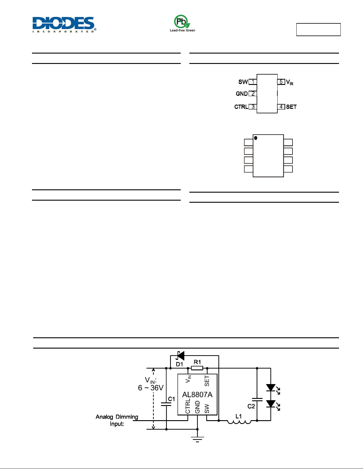
Pin Assignments
(Top View)
SOT25
(Top View)
SET
1
GND
2
GND
3
CTRL
4
MSOP-8EP
Applications
General Illumination Lamps
12V Powered LED Lamps
Wide Analog Dimming Range LED Lamps
V
8
IN
N/C
7
SW
6
SW
5
Typical Applications Circuit
AL8807A
Document number: DS35990 Rev. 2 - 2
1 of 20
www.diodes.com
March 2013
© Diodes Incorporated
A
L8807A
Pin Descriptions
Pin Name
SW 1 5, 6 Switch Pin. Connect inductor/freewheeling diode here, minimizing track length at this pin to reduce EMI.
GND 2 2, 3 GND Pin
CTRL 3 4
SET 4 1 Set Nominal Output Current Pin. Configure the output current of the device.
VIN
EP — EP
N/C — 7 No connection – may be connected to GND.
SOT25 MSOP-8EP
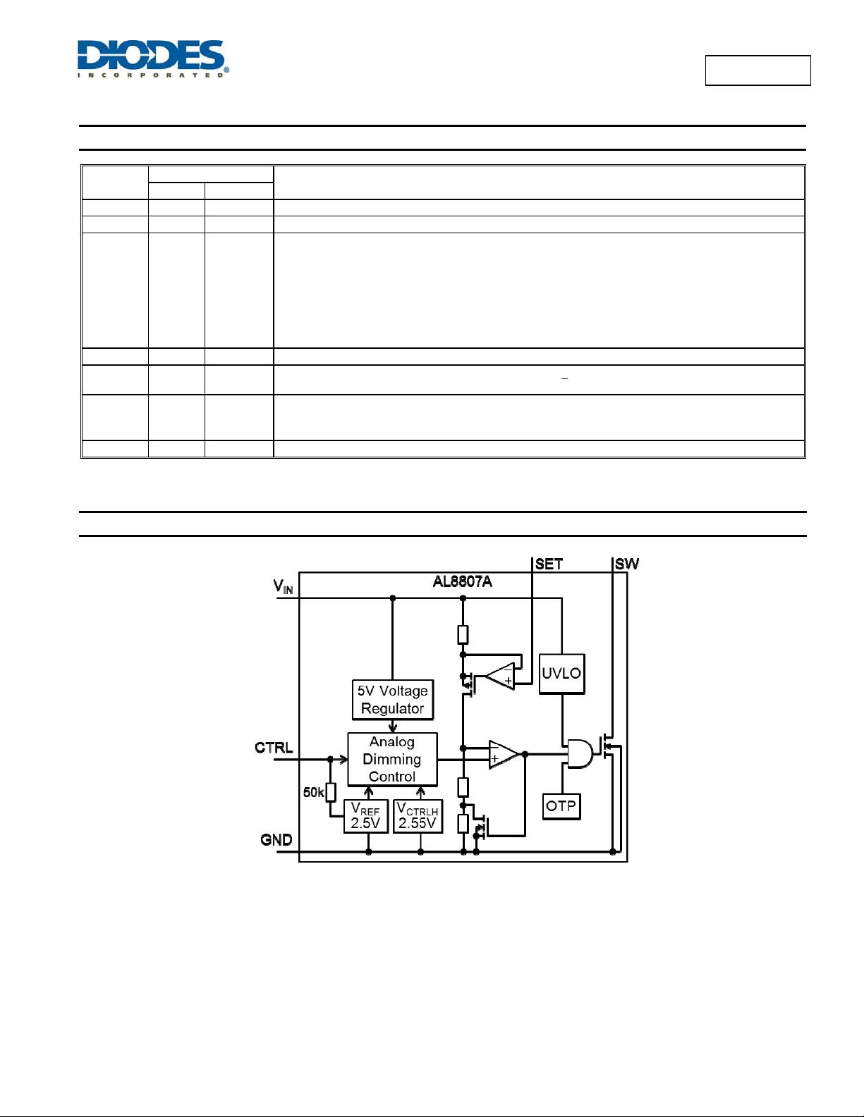
Functional Block Diagram
Pin Number
LED current Analog Dimming Control Input. – No PWM dimming function.
Connected to internal 2.5V V
LED current is achieved - giving nominal average output current I
For Analog dimming drive with analog voltage < 2.5V
(0.25V < V
lower than this level but at reduced accuracy. Some devices will not totally turn off the LED current.
Soft-start can be implemented by connecting a capacitor to CTRL pin. The amount of soft-start is
dependent on ramp-up of input supply voltage and capacitor on CTRL pin. See apps section.
5 8
Input Supply Pin. Must be locally decoupled to GND with >
applications section for more information.
Exposed pad/TAB.
It should be connected to GND and thermal mass for enhanced thermal impedance.
It should not be used as electrical ground conduction path.
Function
via 50k resistor. So if left open circuit V
REF
< 2.5V adjusts output current from 10% to 100% of I
CTRL
OUTnom
OUTnom
2.2µF X7R ceramic capacitor – see
= V
CTRL
= 0.1/RS
. Device will dim the LED current
= 2.5V and 100%
REF
AL8807A
Document number: DS35990 Rev. 2 - 2
2 of 20
www.diodes.com
March 2013
© Diodes Incorporated
A
L8807A
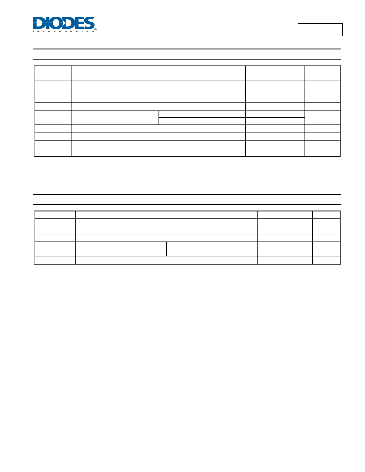
Absolute Maximum Ratings (@T
Symbol Parameter Ratings Unit
ESD HBM Human Body Model ESD Protection 2.5 kV
ESD MM Machine Model ESD Protection 200 V
VIN Continuous VIN Pin Voltage Relative to GND
VSW
V
CTRL
I
SW-RMS
I
SW-PK
TJ
T
LEAD
T
ST
Caution: Stresses greater than the 'Absolute Maximum Ratings' specified above, may cause permanent damage to the device. These are stress ratings only;
SW Voltage Relative to GND -0.3 to +40 V
CTRL Pin Input Voltage -0.3 to +6.0 V
DC or RMS Switch Current
Peak Switch Current (< 10% duty cycle) 2.5 A
Junction Temperature 150 °C
Lead Temperature Soldering 300 °C
Storage Temperature Range -65 to +150 °C
functional operation of the device at these or any other conditions exceeding those indicated in this specification is not implied. Device reliability may be
affected by exposure to absolute maximum rating conditions for extended periods of time.
Semiconductor devices are ESD sensitive and may be damaged by exposure to ESD events. Suitable ESD precautions should be taken when handling
and transporting these devices.
Recommended Operating Conditions (@T
Symbol Parameter Min Max Unit
VIN
V
CTRL
fSW
ISW
TJ
Notes: 4. AL8807A analog dimming range extends below 10% but at reduced LED current accuracies and may not turn completely off. Switching frequencies will
also be increased.
5. Maximum switch current is dependent on power dissipation and junction temperature.
Operating Input Voltage 6.0 36 V
CTRL Pin Input Voltage Range for 10% to 100% ANALOG Dimming (Note 4) 0.25 2.50 V
Maximum Switching Frequency at 100% dimming 0.7 MHz
Continuous Switch Current (Note 5)
Junction Temperature Range -40 +125 °C
= +25°C, unless otherwise specified.)
A
SOT25 1.25
MSOP-8EP 1.5
= +25°C, unless otherwise specified.)
A
SOT25 1
MSOP-8EP 1.3
-0.3 to +40 V
A
A
AL8807A
Document number: DS35990 Rev. 2 - 2
3 of 20
www.diodes.com
March 2013
© Diodes Incorporated
A
L8807A
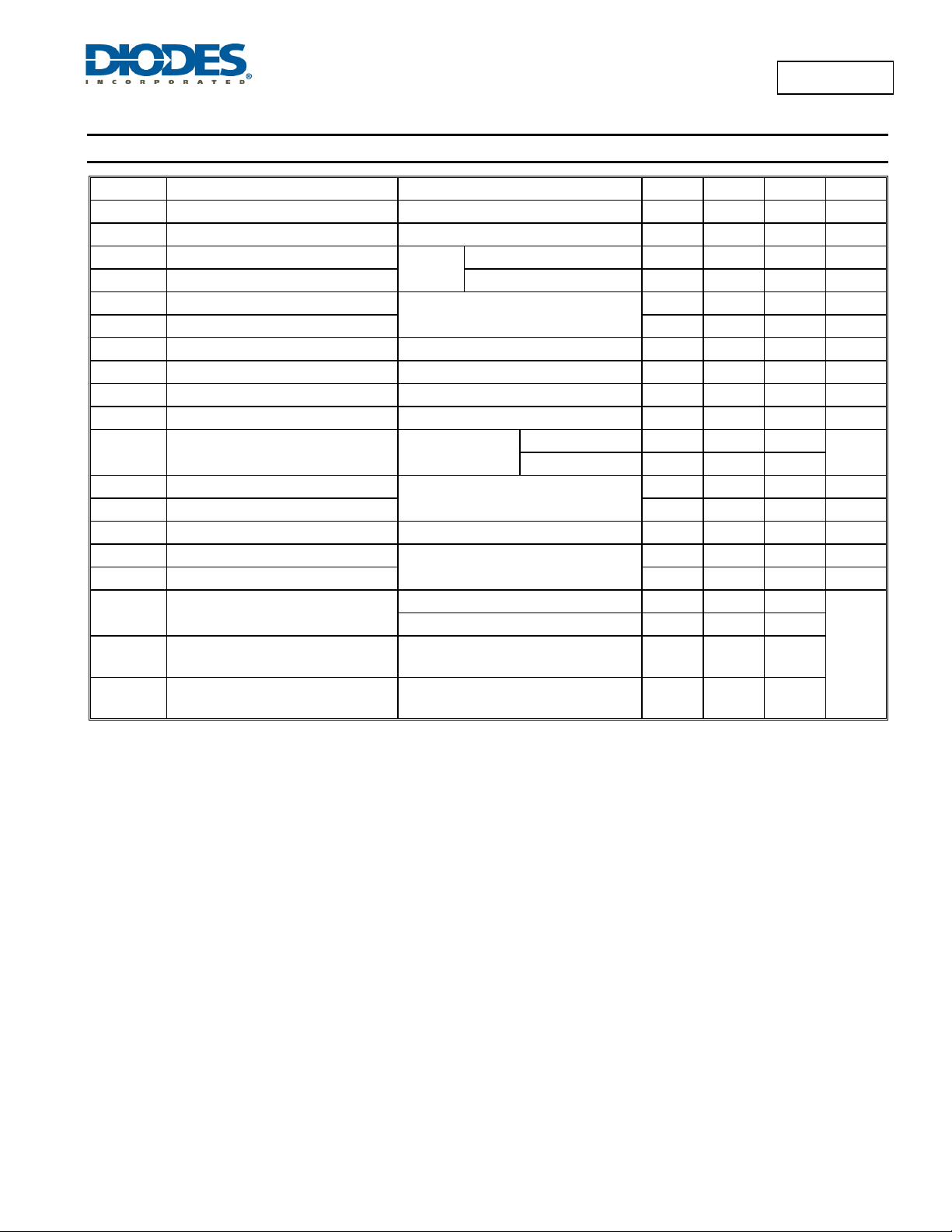
Electrical Characteristics (@T
Symbol Parameter Conditions Min Typ Max Unit
V
INSU
V
INSH
IQ
VTH
V
TH-H
V
TH-10%
I
SET
R
CTRL
V
REF
R
DS(on)
tR
I
SW_Leakage
T
OTP
T
OTP-Hyst
Notes: 6. AL8807A does not have a low power standby mode but current consumption is reduced when output is not being switched.
7. Refer to Figure 40 for the device derating curve.
8. Test condition for SOT25: Device mounted on FR-4 PCB (25mm x 25mm 1oz copper, minimum recommended pad layout on top layer and thermal
vias to bottom layer ground plane. For better thermal performance, larger copper pad for heat-sink is needed.
9. Test condition for MSOP-8EP: Device mounted on FR-4 PCB (51mm x 51mm 2oz copper, minimum recommended pad layout on top layer and
thermal vias to bottom layer with maximum area ground plane. For better thermal performance, larger copper pad for heat-sink is needed.
10. Dominant conduction path via Gnd pin (pin 2).
11. Dominant conduction path via exposed pad.
AL8807A
Document number: DS35990 Rev. 2 - 2
Internal Regulator Start Up Threshold
Internal Regulator Hysteresis Threshold
Quiescent Current
IS
Input Supply Current f = 250kHz 1.8 5 mA
Set Current Threshold Voltage
Set Threshold Hysteresis ±20 %
10% Set Current Threshold Voltage
SET Pin Input Current
CTRL Pin Input Resistance Referred to internal reference 50 k
Internal Reference Voltage 2.5 V
On Resistance of SW MOSFET
SW Rise Time
tF
SW Fall Time 20 ns
Switch Leakage Current
Over-Temperature Shutdown
Over-Temperature Hysteresis 25 C
Thermal Resistance Junction-to-Ambient
JA
(Note 7)
Thermal Resistance Junction-to-Lead
JL
(Note 10)
Thermal Resistance Junction-to-case
JC
(Note 11)
= +25°C, unless otherwise specified.)
A
VIN rising
VIN falling
CTRL pin
Output not switching (Note 6) 350 µA
floating
CTRL pin floating
V
= 0.25V
CTRL
V
= V
SET
ISW = 0.3A
V
SENSE
V
SW
-0.1
IN
SOT25 0.25 0.40
MSOP-8EP 0.18 0.35
= 100 ±20mV, fSW = 250kHz
= 0.1V ~ 12V ~ 0.1V, CL = 15pF
VIN = 36V
SOT25 (Note 8) 250
MSOP-8EP (Note 9) 69
SOT25 (Note 8) 50
MSOP-8EP (Note 9) 4.3
4 of 20
www.diodes.com
5.9 V
100 300 mV
95 100 105 mV
4 10 15 mV
16 22 µA
12 ns
0.5 A
150 C
°C/W
March 2013
© Diodes Incorporated
A
R
R
Typical Performance Characteristics
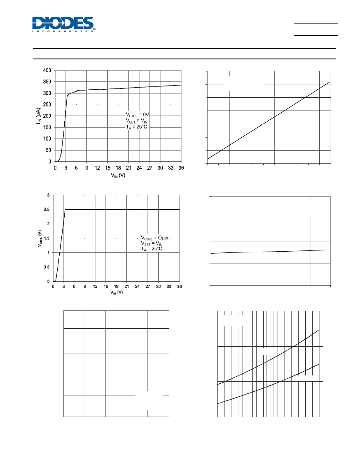
Figure 1 Supply Current (not switching) vs. Input Voltage
(@TA = +25°C, unless otherwise specified.)
80
V
= VIN = 12V
60
SET
= 25°C
T
A
40
20
(µA)
0
CTRL
I
-20
-40
-60
0.0 0.5 1.0 1.5 2.0 2.5 3.0 3.5 4.0 4.5 5.0 5.5
Figure 2 I
V
CTRL
CTRL
(V)
vs. V
CTRL
L8807A
(m )
300
240
180
DS(ON)
120
Figure 3 V
vs Input Voltage
CTRL
(CTRL pin open circuit)
MSOP-8EP
SOT25
2.52
V
= Open
CTRL
= VIN = 12V
V
SET
2.51
(V)
2.50
CTRL
V
2.49
2.48
-40 -15 10 35 60 85 110
Ambient Temperature (°C)
400
Figure 4 V
V = Open
CTRL
V = V = 12V
SET IN
vs. Temperature
CTRL
350
300
(m )
250
DS(ON)
200
SOT25
MSOP-8EP
60
0
61218243036
INPUT VOLTAGE
Figure 5 SW R vs. Input Voltage
AL8807A
Document number: DS35990 Rev. 2 - 2
DS(ON)
V = Open
CTRL
V = V
SET IN
T = 25°C
A
5 of 20
www.diodes.com
150
100
-40 10 35 60 85 110
-15
AMBIENT TEMPERATURE (°C)
Figure 6 SW R vs. Temperature
DS(ON)
© Diodes Incorporated
March 2013
A
CUR
REN
T ERRO
R
CUR
RENT
C
URREN
T
Typical Performance Characteristics
(cont.) (@TA = +25°C, unless otherwise specified.)
L8807A
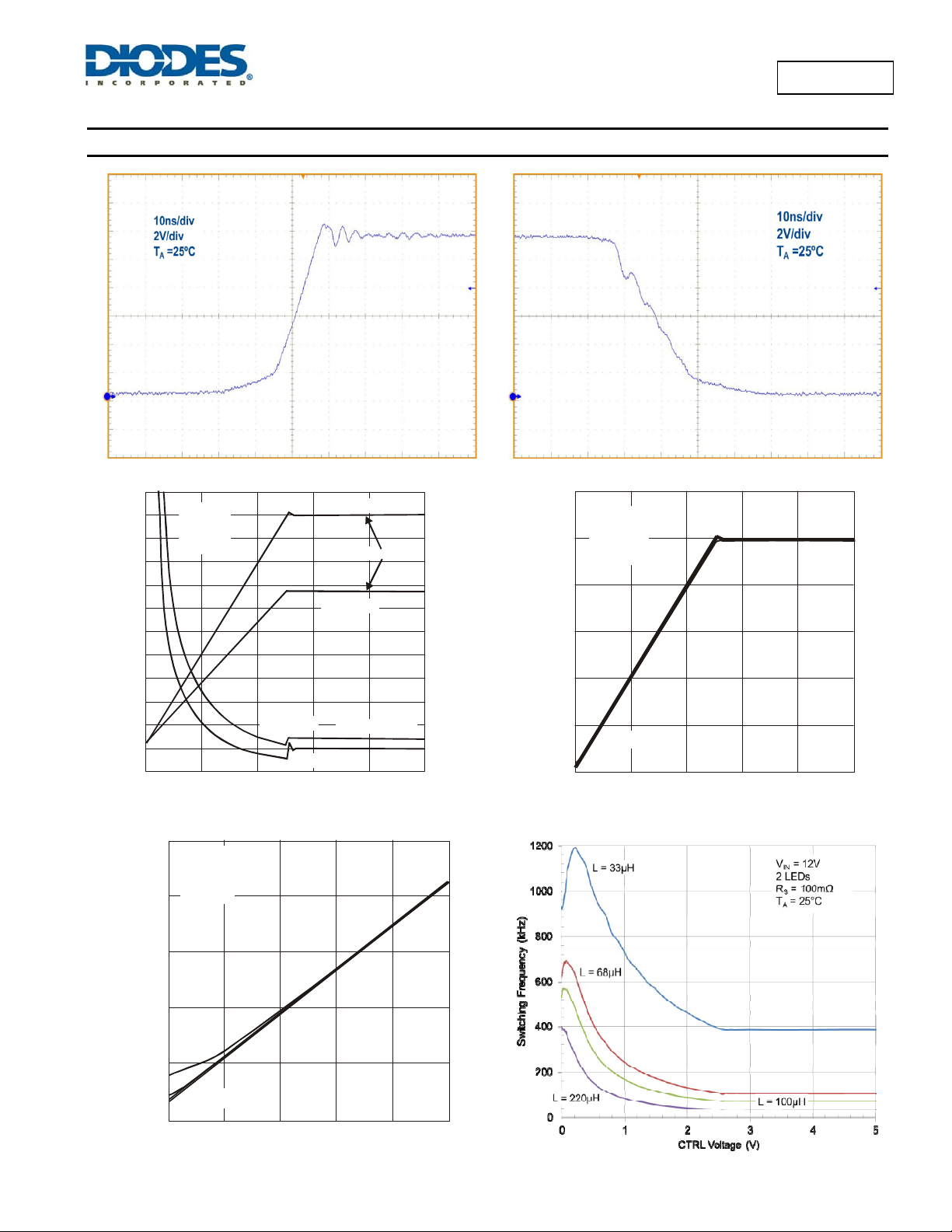
Figure 7 SW Output Rise Time
22%
R = 100m
S
LED Current
(%)
20%
18%
16%
V = 12V
IN
2 LEDs
L = 68µH
T = 25°C
A
14%
R = 150m
12%
S
10%
8%
6%
4%
LED
2%
0%
-2%
012345
R = 150m
S
LED Current Error
R = 100m
S
CTRL VOLTAGE (V)
Figure 9 LED Current (Different Sense Resistor) vs. V
0.25
V = 12V
IN
2 LEDs
R = 100m
S
T = 25°C
A
0.20
1.10
1.00
0.90
0.80
0.70
0.60
0.50
0.40
0.30
0.20
0.10
0.00
-0.10
CTRL
Figure 8 SW Output Fall Time
1.2
V = 12V
IN
2 LEDs
1.0
0.8
(A)
R = 100m
S
T = 25°C
A
0.6
L = 33µH
LED CURRENT (A)
0.4
LED
0.2
L = 68 ~ 220µH
0.0
012345
CTRL VOLTAGE (V )
Figure 10 LED Current (Different Inductor) vs. V
CTRL
(A)
0.15
0.10
LED
L = 33µH
0.05
L = 68 ~ 220µH
0.00
0 0.1 0.2 0.3 0.4 0.5
Figure 11 LED Current (Zoomed In) vs. V
AL8807A
Document number: DS35990 Rev. 2 - 2
CTRL
6 of 20
www.diodes.com
Figure 12 Switching Frequency vs. V
CTRL
March 2013
© Diodes Incorporated
CTRL PIN VOLT AGE (V)
 Loading...