

Page 1
A
L8806
HIGH EFFICIENCY 36V 1.5A BUCK LED DRIVER
Description
The AL8806 is a step-down DC/DC converter designed to drive LEDs
with a constant current. The device can drive up to 8 LEDs,
depending on the forward voltage of the LEDs, in series from a
voltage source of 6V to 36V. The AL8806 switches at frequencies up
to 1MHz. This allows the use of small size external components,
hence minimizing the PCB area needed.
Maximum output current of AL8806 is set via an external resistor
connected between the V
by applying either a DC voltage or a PWM signal at the CTRL input
pin. An input voltage of 0.4V or lower at CTRL switches off the output
MOSFET simplifying PWM dimming.
and SET input pins. Dimming is achieved
IN
Features
LED driving current up to 1.5A
Better than 5% accuracy
High efficiency up to 98%
Operating input voltage from 6V to 36V
High switching frequency up to 1MHz
PWM/DC input for dimming control
Built-in output open-circuit protection
MSOP-8EP: Available in “Green” Molding Compound (No Br,
Sb) with lead Free Finish/ RoHS Compliant
Totally Lead-Free & Fully RoHS Compliant (Notes 1 & 2)
Halogen and Antimony Free. “Green” Device (Note 3)
Notes: 1. No purposely added lead. Fully EU Directive 2002/95/EC (RoHS) & 2011/65/EU (RoHS 2) compliant.
2. See http://www.diodes.com/quality/lead_free.html for more information about Diodes Incorporated’s definitions of Halogen- and Antimony-free, "Green"
and Lead-free.
3. Halogen- and Antimony-free "Green” products are defined as those which contain <900ppm bromine, <900ppm chlorine (<1500ppm total Br + Cl) and
<1000ppm antimony compounds.
Pin Assignments
SET
SET
GND
GND
GND
GND
CTRL
CTRL
Applications
High Power MR16 Lamps
General Illumination Lamps
Multi-Die LED Driver
1
1
2
2
AL8806
AL8806
3
3
4
4
MSOP-8EP
V
V
8
8
IN
IN
7
7
N/C
N/C
6
6
SW
SW
5
5
SW
SW
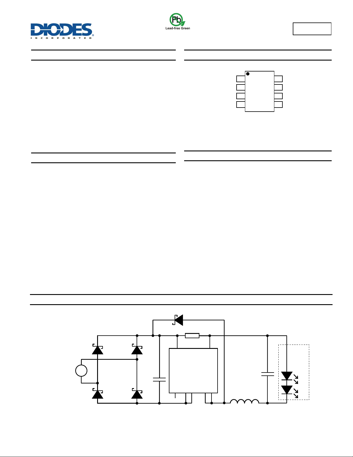
Typical Applications Circuit
D2 D3
DFLS230LH
12V
~
AC
x4
D4 D5
AL8806
Document number: DS35144 Rev. 5 - 2
C1
450µF
DFLS230LH
D1
R
SET
0R089
IN
V
AL8806
CTRL
GND
1 of 15
www.diodes.com
SET
SW
33µH L1
C2
1µF
Multi-
die
LED
July 2013
© Diodes Incorporated
Page 2
A
Pin Descriptions
Pin Number
Pin
Name
GND 2, 3 GND Pin
CTRL 4
SET 1 Set Nominal Output Current Pin. Configure the output current of the device.
N/C 7 no connection
MSOP-8EP
SW 5, 6 Switch Pin. Connect inductor/freewheeling diode here, minimizing track length at this pin to reduce EMI.
Dimming and On/Off Control Input.
Leave floating for normal operation.
(V
= V
= 2.5V giving nominal average output current I
REF
< 2.5V) to adjust output current from 20% to 100% of I
CTRL
Drive to voltage below 0.4V to turn off output current
Drive with DC voltage (0.5V < V
A PWM signal (low level ≤ 0.4V and high level > 2.6; transition times less than 1us) allows the output current to be
VIN
EP EP
8
Input Supply Pin. Must be locally decoupled to GND with >
more information.
Exposed pad:
Connect to GND and thermal mass for enhanced thermal impedance. It should not be used as electrical ground
conduction path.
CTRL
adjusted below the level set by the resistor connected to SET input pin.
Function
= 0.1/RS)
OUTnom
OUTnom
2.2µF X7R ceramic capacitor – see applications section for
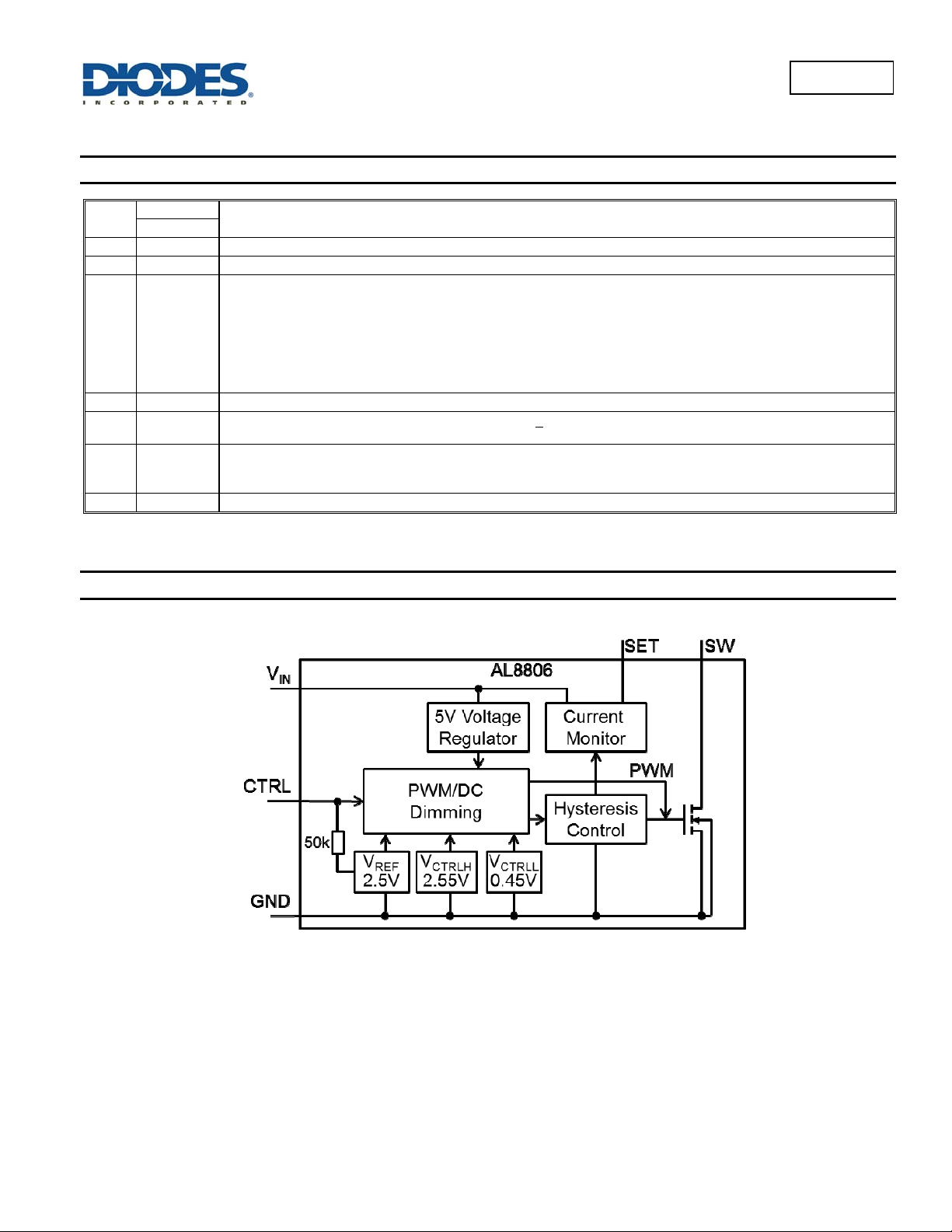
Functional Block Diagram
L8806
AL8806
Document number: DS35144 Rev. 5 - 2
2 of 15
www.diodes.com
July 2013
© Diodes Incorporated
Page 3
A
L8806
Absolute Maximum Ratings (@T
Symbol Parameter Ratings Unit
ESD HBM Human Body Model ESD Protection 2.5 kV
ESD MM Machine Model ESD Protection 200 V
VIN Continuous VIN pin voltage relative to GND
VSW
V
CTRL
I
SW-RMS
I
SW-PK
TJ
T
LEAD
T
ST
Caution: Stresses greater than the 'Absolute Maximum Ratings' specified above, may cause permanent damage to the device. These are stress ratings only;
SW voltage relative to GND -0.3 to +40 V
CTRL pin input voltage -0.3 to +6 V
DC or RMS switch current 1.65 A
Peak switch current (<10%) 3 A
Junction Temperature 150 °C
Lead Temperature Soldering 300 °C
Storage Temperature Range -65 to +150 °C
functional operation of the device at these or any other conditions exceeding those indicated in this specification is not implied. Device reliability may be
affected by exposure to absolute maximum rating conditions for extended periods of time.
Semiconductor devices are ESD sensitive and may be damaged by exposure to ESD events. Suitable ESD precautions should be taken when handling
and transporting these devices.
Recommended Operating Conditions (@T
Symbol Parameter Min Max Unit
VIN
V
CTRLH
V
CTRLDC
V
CTRLL
ISW
f
OSC
TJ
Operating Input Voltage relative to GND 6.0 36 V
Voltage High for PWM dimming relative to GND 2.6 5.5 V
Voltage range for 20% to 100% DC dimming relative to GND 0.5 2.5 V
Voltage Low for PWM dimming relative to GND 0 0.4 V
DC or RMS switch current 1.5 A
Switching Frequency 1 MHz
Junction Temperature Range -40 +125 °C
Electrical Characteristics (@V
Symbol Parameter Conditions Min Typ Max Unit
V
INSU
V
INSH
IQ
IS
VTH
V
TH-H
I
SET
R
CTRL
V
REF
R
DS(on)
I
SW_Leakage
JA
JC
Notes: 4. AL8806 does not have a low power standby mode but current consumption is reduced when output switch is inhibited: V
tested with V
5. Dominant conduction path via exposed pad. Refer to figure 5 for the device derating curve.
6. Measured on an FR4 51x51mm PCB with 2oz copper standing in still air with minimum recommended pad layout on top layer and thermal vias to
bottom layer maximum area ground plane. For better thermal performance, larger copper pad for heat-sink is needed.
Internal regulator start up threshold
Internal regulator hysteresis threshold
Quiescent current Output not switching
Input supply Current CTRL pin floating f = 250kHz 1.8 5 mA
Set current Threshold Voltage
Set threshold hysteresis ±20 mV
SET pin input current
CTRL pin input resistance Referred to internal reference 50 kΩ
Internal Reference Voltage 2.5 V
On Resistance of SW MOSFET
Switch leakage current
Thermal Resistance Junction-to-Ambient (Note 5) MSOP-8EP (Note 6) 69
Thermal Resistance Junction-to-Case (Note 5) MSOP-8EP (Note 6) 4.3
≤ 2.5V
CTRL
= +25°C, unless otherwise specified.)
A
-0.3 to +40 V
= +25°C, unless otherwise specified.)
A
= 12V, TA = +25°C, unless otherwise specified.)
IN
VIN rising
VIN falling
(Note 4) 350 µA
V
≥ 2.6V or floating.
CTRL
V
= VIN-0.1
SET
ISW = 1A
VIN =36V
5.9 V
100 300 mV
95 100 105 mV
16 22 µA
0.18 0.35 Ω
0.5 μA
C/W
= 0V. Parameter is
SENSE
AL8806
Document number: DS35144 Rev. 5 - 2
3 of 15
www.diodes.com
July 2013
© Diodes Incorporated
Page 4
A
0
CUR
RENT
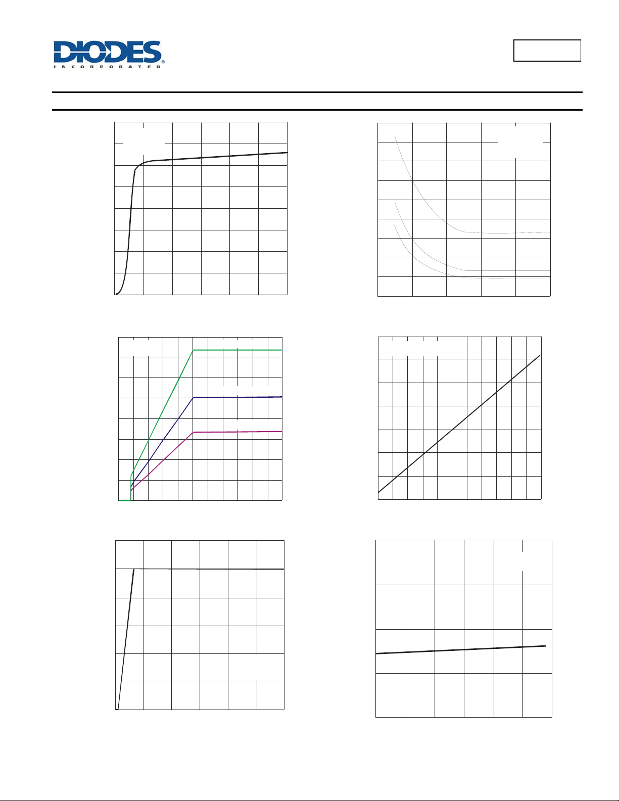
Typical Performance Characteristics
40
V = 0V
CTRL
V = V
350
SET IN
°
T = 25C
A
300
250
200
IN
I (µA)
150
100
50
0
0 5 10 15 20 25 30
V (V)
IN
Supply Current (not switching) vs. Input Current
1.6
1.4
T = 25°C
A
L =68µH
R = 68m
SET
L8806
900
L = 33µ H
800
700
600
L = 68µ H
500
400
Frequency (kHz)
300
200
L = 100 µ H
100
0
012345
80
60
Switching Frequency vs. V
V = V = 12V
SET IN
T = 25C
A
V(V)
CTR L
V = 12V
IN
1 LED
R = 150m
SET
T = 25°C
A
CTRL
1.2
R = 100m
(A)
1
0.8
SET
R = 150m
SET
0.6
LED
0.4
0.2
0
0 0.5 1 1.5 2 2.5 3 3.5 4 4.5 5 5.5
CTRL VOLTAGE (V)
2.5
1.5
CTRL
V (V)
0.5
LED Current vs. V
3
2
1
CTRL
V= Open
CTRL
V = V
SET IN
T = 25C
A
40
20
CTRL
I (µA)
0
-20
-40
-60
0.0 0.5 1.0 1.5 2.0 2.5 3.0 3.5 4.0 4.5 5.0 5.5
V (V)
CTRL
I vs V
CTRL CTRL
2.52
V = Open
CTRL
V = V = 12V
SET IN
2.51
2.50
CTRL
V (V)
2.49
0
0 5 10 15 20 25 30
V (V)
V vs. Input Voltage
(CTRL pin open circuit)
IN
CTRL
2.48
-40 -15 10 35 60 85 110
Ambient Temperature (°C)
V vs. Temperature
CTRL
AL8806
Document number: DS35144 Rev. 5 - 2
4 of 15
www.diodes.com
July 2013
© Diodes Incorporated
Page 5
A
R (m
%
Typical Performance Characteristics (cont.)
5.0
V = 12V
4.5
4.0
IN
1 LE D
R = 150m
SET
L = 68µ H
3.5
3.0
2.5
LED Current E rror
2.0
I
1.5
LED Current Error (%)
LED
1.0
0.5
0.0
0% 20% 40% 60% 80% 100%
PWM Duty Cycle
I vs. PWM Duty Cycle
LED
260
240
220
)
200
180
DS(ON)
160
140
120
100
-40 -15 10 35 60 85 110
V = Open
CTRL
V = V 12V
SET IN
AMBIENT TEMPERATURE (°C)
SW R vs. Temperature
DS(ON)
100
90%
80%
L = 33µ H
R = 150m
SET
T = 25C
A
2 LE D
70%
1
0.9
0.8
0.7
0.6
0.5
0.4
0.3
0.2
0.1
0
L8806
200
180
160
140
120
100
DS(ON)
80
LED Current (A)
R (m)
60
40
20
0
051015
R vs. Input Voltage
DS(ON)
V (V)
IN
V = Open
CTRL
V = V 12V
SET IN
T = 25C
A
20 25 30
130
125
120
V
SEN SE
115
V
110
SW
105
SENSE
100
V (mV)
95
90
85
80
02468
R = 150m
SET
L = 68µ H
V = 12V
IN
1 LED Load
Time (µs)
SW Output Switching Characteristics
18
16
14
12
10
8
6
4
2
0
-2
SW
V
60%
50%
Duty Cycle
40%
30%
20%
10%
0%
6 9 12 15 18 21 24 27 30
Input Voltage (V)
Duty Cycle vs. Input Voltage
AL8806
Document number: DS35144 Rev. 5 - 2
5 of 15
www.diodes.com
July 2013
© Diodes Incorporated
Page 6

A
%
%
%
Typical Operating Performance Characteristics (cont.)
10
8%
6%
4%
2%
0%
-2%
% ERROR
-4%
-6%
-8%
-10%
700
600
1.5A Nominal LED Current 1.0A Nominal LED Current
5 LEDs
6 LEDs
7 LEDs
8 LEDs
2 LEDs
3 LEDs
1 LED
T = 25°C
A
L = 33µH
R = 66.67m
S
4 LEDs
6 9 12 15 18 21 24 27 30
T = 25°C
A
L = 33µH
R = 66.67m
S
INPUT VOLTAGE (V)
10
8%
6%
4%
2 LEDs
3 LEDs
4 LEDs
5 LEDs
6 LEDs
7 LEDs
2%
1 LED
0%
-2%
DEVIATION
-4%
-6%
T = 25°C
A
L = 33µH
-8%
R = 100m
-10%
6 9 12 15 18 21 24 27 30
S
INPUT VOLTAGE (V)
700
T = 25°C
A
L = 33µH
600
R = 100m
S
L8806
8 LEDs
500
400
300
200
1 LED
100
SWITCHING FREQUENCY (kHZ)
0
2 LEDs
3 LEDs
4 LEDs 5 LEDs
6 LEDs 7 LEDs
6 9 12 15 18 21 24 27 30
INPUT VOLTAGE (V)
100%
7 LEDs
6 LEDs
5 LEDs
4 LEDs
95%
3 LEDs
2 LEDs
90%
85%
1 LED
80%
T = 25°C
A
L = 33µH
R = 66.67m
75%
S
6 9 12 15 18 21 24 27 30
INPUT VOLTAGE (V)
8 LEDs
8 LEDs
500
400
300
200
1 LED
SWITCHING FREQUENCY (kHz)
100
2 LEDs
3 LEDs
4 LEDs
5 LEDs
6 LEDs
0
7 LEDs
6 9 12 15 18 21 24 27 30
INPUT VOLTAGE (V)
100
95%
2 LEDs
3 LEDs
4 LEDs
5 LEDs
6 LEDs
7 LEDs
90%
1 LED
85%
EFFICIENCY
80%
T = 25°C
A
L = 33µH
R = 100m
75%
6 9 12 15 18 21 24 27 30
S
INPUT VOLTAGE (V)
8 LEDs
8 LEDs
AL8806
Document number: DS35144 Rev. 5 - 2
6 of 15
www.diodes.com
July 2013
© Diodes Incorporated
Page 7

A
L8806
Application Information
AL8806 Operation
In normal operation, when voltage is applied at VIN, the AL8806 internal switch is turned on. Current starts to flow through sense resistor R
inductor L1, and the LEDs. The current ramps up linearly, and the ramp rate is determined by the input voltage V
DFLS230LH
DFLS230LH
D1
12V
12V
GND
GND
C1
C1
4.7µF
4.7µF
C2
C2
100nF
100nF
D1
R
R
SET
SET
0R082
0R082
IN
IN
V
V
AL8806
AL8806
CTRL
CTRL
GND
GND
SET
SET
SW
SW
33µH
C3
C3
1µF
1µF
L1
Figure 1 Typical Application Circuit
This rising current produces a voltage ramp across R
proportional voltage to the input of the internal comparator.
When this voltage reaches an internally set upper threshold, the internal switch is turned off. The inductor current continues to flow through R
L1, the LEDs and the schottky diode D1, and back to the supply rail, but it decays, with the rate of decay determined by the forward voltage drop of
the LEDs and the schottky diode.
This decaying current produces a falling voltage at R
applied at the input of the internal comparator. When this voltage falls to the internally set lower threshold, the internal switch is turned on again.
This switch-on-and-off cycle continues to provide the average LED current set by the sense resistor R
. The internal circuit of the AL8806 senses the voltage across R
SET
, which is sensed by the AL8806. A voltage proportional to the sense voltage across R
1
.
SET
and the inductor L1.
IN
Multi-
Multi-
die
die
LED
LED
and applies a
SET
LED Current Control
The LED current is controlled by the resistor R
Connected between V
If the CTRL pin is driven by an external voltage (higher than 0.4V and lower than 2.5V), the average LED current is:
For example for a desired LED current of 1.33A and a default voltage V
and SET the nominal average output current in the LED(s) is defined as:
IN
in Figure 1.
SET
R
SET
V
I
LED
THD
I
LED
V
V
THD
I
LED
V
CTRL
CTRL
V
REF
V
R
SET
V
CTRL
THD
R
SET
REF
=2.5V the resulting resistor is:
5.2
1.0
5.2
33.1
m75
DC Dimming
The CTRL pin can be driven by an external DC voltage (V
. The LED current decreases linearly with the CTRL voltage when 0.5V ≤ V
R
SET
Note that 100% brightness setting corresponds to V
the device will not overdrive the LED current and will still set the current according to the equation V
When the CTRL voltage falls below the threshold, 0.4V, the output switch is turned off which allows PWM dimming.
CTRL
), to adjust the output current to a value below the nominal average value defined by
CTRL
≤ 2.5V, as shown on page 4 for 4 different current levels.
CTRL
= V
, nominally 2.5V. For any voltage applied on the CTRL pin that is higher than V
REF
= V
REF
.
CTRL
SET
SET
SET
is
REF
,
,
,
AL8806
Document number: DS35144 Rev. 5 - 2
7 of 15
www.diodes.com
July 2013
© Diodes Incorporated
Page 8

A
]
]
L8806
Application Information (cont.)
PWM Dimming
LED current can be adjusted digitally, by applying a low frequency Pulse Width Modulated (PWM) logic signal to the CTRL pin to turn the device on
and off. This will produce an average output current proportional to the duty cycle of the control signal. In particular, a PWM signal with a max
resolution of 10bit can be applied to the CTRL pin to change the output current to a value below the nominal average value set by resistor R
achieve this resolution the PWM frequency has to be lower than 500Hz, however higher dimming frequencies can be used - at the expense of
dimming dynamic range and accuracy.
Typically, for a PWM frequency of 500Hz the accuracy is better than 1% for PWM ranging from 1% to 100%.
700
600
500
400
SET
. To
300
200
LED curre nt [m A
100
0
0% 10% 20% 30% 40% 50% 60% 70% 80% 90% 100%
PWM dim m ing [%]
Figure 2 PWM Dimming at 500Hz
70
60
50
40
30
20
LED current [mA
10
0
0% 1% 2% 3% 4% 5% 6% 7% 8% 9% 10%
PW M dim m ing [%]
Figure 3 Low Duty Cycle PWM Dimming at 500Hz
The PWM pin is designed to be driven by both 3.3V and 5V logic levels directly from a logic output with either an open drain output or push-pull
output stage.
AL8806
Document number: DS35144 Rev. 5 - 2
8 of 15
www.diodes.com
© Diodes Incorporated
July 2013
Page 9

A
L8806
Application Information (cont.)
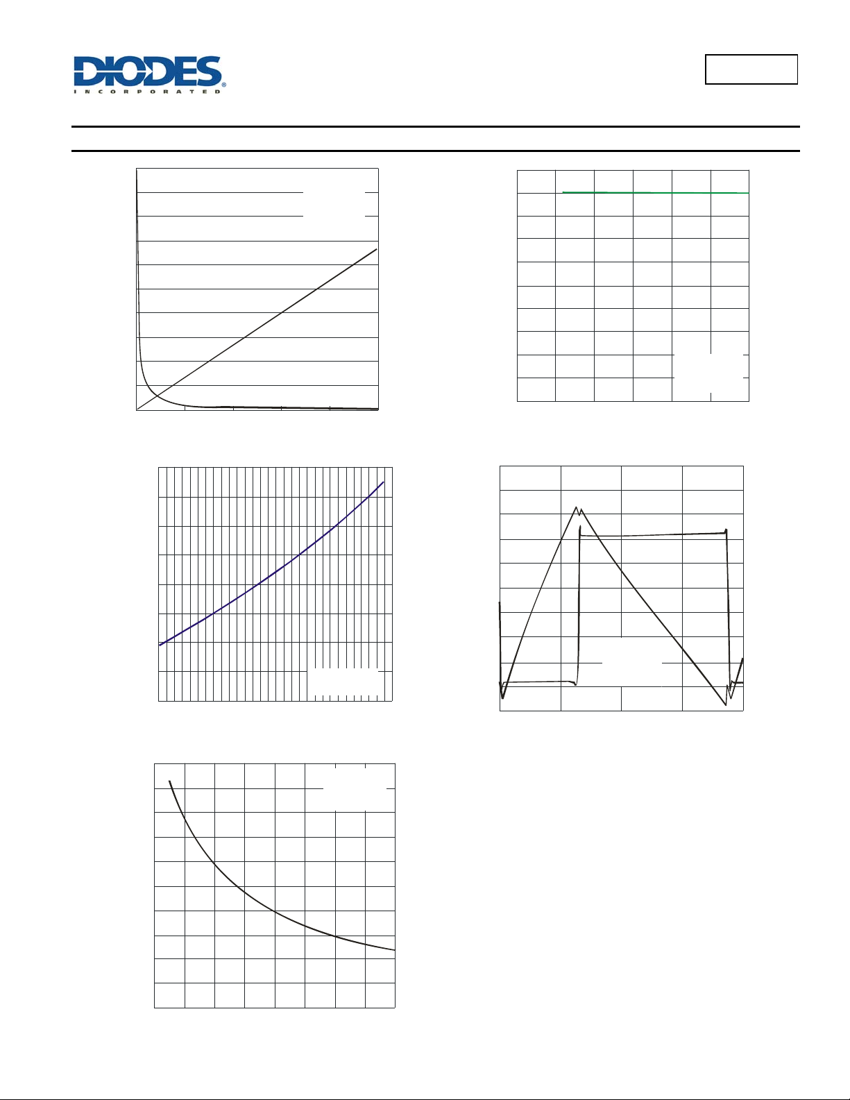
Soft Start
The AL8806 does not have in-built soft-start action – this provides very fast turn off of the output the stage improving PWM dimming accuracy;
nonetheless, adding an external capacitor from the CTRL pin to ground will provide a soft-start delay. This is achieved by increasing the time taken
for the CTRL voltage to rise to the turn-on threshold and by slowing down the rate of rise of the control voltage at the input of the comparator.
Adding a capacitor increases the time taken for the output to reach 90% of its final value, this delay is 0.1ms/nF, but will impact on the PWM
dimming accuracy depending on the delay introduced.
Figure 4 Soft Start with 22nF Capacitor on CTRL Pin (V
= 36V, I
IN
= 667mA, 1 LED)
LED
Reducing Output Ripple
Peak to peak ripple current in the LED(s) can be reduced, if required, by shunting a capacitor C2 a cross the LED(s) as shown al ready in the circuit
schematic.
A value of 1μF will reduce the supply ripple current by a factor three (approx.). Proportionally lo wer ripple can be achieved with higher capacitor
values. Note that the capacitor will not affect operating frequency or efficiency, but it will increase start-up delay, by reducing the rate of rise of
LED voltage. By adding this capacitor the current waveform through the LED(s) changes from a triangular ramp to a more sinusoidal version
without altering the mean current value.
AL8806
Document number: DS35144 Rev. 5 - 2
9 of 15
www.diodes.com
July 2013
© Diodes Incorporated
Page 10

A
L8806
Application Information (cont.)
Capacitor Selection
The small size of ceramic capacitors makes them ideal for AL8806 applications. X5R and X7R types are recommended because they retain their
capacitance over wider voltage and temperature ranges than other types such as Z5U.
A 2.2μF input capacitor is sufficient for most intended applications of AL8806; however a 4.7μF input capacitor is suggested for input voltages
approaching 30V.
Diode Selection
For maximum efficiency and performance, the rectifier (D1) should be a fast low capacitance Schottky diode with low reverse leakage at the
maximum operating voltage and temperature. The Schottky diode also provides better efficiency than silicon PN diodes, due to a combination of
lower forward voltage and reduced recovery time.
It is important to select parts with a peak current rating above the peak coil current and a continuous current rating higher t h an th e maximum outpu t
load current. In particular, it is recommended to have a diode voltage rating at least 15% higher than the operating voltage to ensure safe operation
during the switching and a current rating at least 10% higher than the average diode current. The power rating is verified by calculating the power
loss through the diode.
Schottky diodes, e.g. B240 or B140, with their low forward voltage drop and fast reverse recovery, are the ideal choice for AL8806 applications.
Thermal and Layout Considerations
For continuous conduction mode of operation, the absolute maximum junction temperature must not be exceeded. The maximum p o wer dissipation
depends on several factors: the thermal resistance of the IC package
and ambient temperature.
The maximum power dissipation can be calculated using the following formula:
where T
is the maximum operating junction temperature,
J(MAX)
, PCB layout, airflow surrounding the IC, and difference between junction
JA
T
The recommended maximum operating junction temperature, T
junction to ambient thermal resistance,
enhanced MSOP-8EP package.
, is layout dependent and the AL8806’s JA in MSOP-8EP on a
JA
51 x 51mm double layer PCB with 2oz copper standing in still air is
approximately 69°C/W.
Therefore the maximum power dissipation at T
Figure 5, shows the power derating of the AL8806 on an FR4
51x51mm PCB with 2oz copper standing in still air.
As the ambient temperature increases and/or the PCB area reduces
the maximum allowable power dissipated by the AL8806 will
decrease.
AL8806
Document number: DS35144 Rev. 5 - 2
is the ambient temperature, and
A
is the junction to ambient thermal resistance.
JA
. To support high LED drive at higher ambient temperatures the AL8806 has been packaged in thermally
JA
= +25°C is:
A
P
)MAX(D
C25C125
W/C69
, is 125°C and so maximum ambient temperature is determined by the AL8806’s
J
W45.1
www.diodes.com
10 of 15
1600
1400
1200
1000
800
600
400
Power di s si pa t i on ( m W )
200
0
-40 -25 -10 5 20 35 50 65 80 95 110 125
MSOP-8EP
Ambient tem per at ure ( ° C)
Figure 5 Derating Curve
July 2013
© Diodes Incorporated
Page 11

A
L8806
Application Information (cont.)
PCB Layout
When laying out the PCB for the AL8806 the following should be observed:
1. The decoupling capacitor C1 has to be placed as close as possible to V
2. The sense resistor, R
3. The anode of the freewheel diode (D1), the SW pin and the inductor have to be placed as close as possible to each other to avoid ringing.
, has to be placed as close as possible to VIN and SET
SET
R
SET
IN
To avoid
radiated EMI
keep dashed
tracks as
short as
possible
IN
V
AL8806
SET
D1
C2
C1
CTRL
GND
SW
L1
Figure 6 PCB Layout
The AL8806 has two evaluation boards available on request (AL8806EV4 and AL8806EV6). Information can be found on the Diodes website and
from a Diodes’ sales representative.
Application Example
A typical application example for the AL8806 is the MR16 lamp; which normally operate from 12VDC or 12VAC supplies, using conventional
electromagnetic transformers or electronic transformers.
As a replacement for MR16 halogen lamps, LED lamps offer a more energy efficient solution - radiating no h eat and no Ultra Violet light. The l ow
thermal impedance of the AL8806 and its 1.5A switch capability allows it drive some of the latest multi-die LEDs; which increases the lamp’s
luminance.
This application example is intended to fit into the base connector space of an MR16 style LED lamp . The design has been optimized f or pa rt coun t
and thermal performance for a multi-die LED in the Lens section as well as EMI conformance.
AL8806
Document number: DS35144 Rev. 5 - 2
Figure 7 MR16 Schematic
11 of 15
www.diodes.com
July 2013
© Diodes Incorporated
Page 12

A
L8806
Application Information (cont.)
Application Example
The output of the 12V transformer is fed into the bridge rectifier, comprising of D2, D3, D4 and D5. C10 offers an optional EMI filtering at the input.
(see figure 9)
Capacitor, C
used to sustain operation of the device during the low part of the rectified AC wave. In the case of a system driving two LEDs at 1.1A, one 470µF
plus 47µF capacitors are required.
Capacitors C3 and C9 provide local decoupling for the AL8806 and for the schottky freewheeling diode, D1. It is important that C3 i s as close as
possible to the AL8806’s V
The LED current is determined by the total resistance between the V
BOM).
C4 decouples the LED connections, again to minimize EMI, as well as smoothing the current.
D1 operates as the freewheeling diode, providing a current path for the LED current when the power switch at SW pin is off.
Capacitors C5 to C9, 1.5nF have been added to improve the overall EMI performa nce. C5 is connected across the Suppl y pins to reduce radiation
via the wiring. C6 and C7 also assist the reduction of EMI via the wiring. C8 snubs high frequency radiation f rom the harmonics in the switching
regulator.
A large number of vias have been used to improve the grounding effect throughout the PCB to improve the evaluation board’s EMI performance.
BULK
(cont.)
, (capacitors C1 and C2 on the PCB and BOM are multiple components to reduce size) forms the bulk reservoir capacitance -
pin and that C9 is as close to the VIN and shottky diode as possible, as reflected in the layout shown below in figure 8.
IN
and SET pins (R1 and R2 in figures 7 (schematic) and 8 (top PCB) and
IN
Figure 8 AL8806EV6 evaluation board (Top)
AL8806
Document number: DS35144 Rev. 5 - 2
12 of 15
www.diodes.com
Figure 9 AL8806EV6 evaluation board (Bottom)
© Diodes Incorporated
July 2013
Page 13

A
L8806
Application Information (cont.)
AL8806EV6 BOM
Count Designator Description Package Manufacturer Part Number
1 C1 Capacitor, 470uF, 25V Aluminium Electrolytic
1 C2 Capacitor, 4.7µF 10% 50V X7R 1210 Kemet C1210X475K5RAC
3 C3, C9, C10 Capacitor, 100nF 10% 50V X7R 0805
1 C4 Capacitor, 100nF 10% 50V X7R 1206
4 C5 to C8 Capacitor, 1.5nF 10% 50V or 100V, COG 0805 generic
1 L1 Inductor, shielded, 15µH 20% 6.6 x 6.6mm
1 L2 Inductor, ferrite bead, 6A, 30ohms @100MHz 0805 TDK MPZ2012S300A
1 R1 Resistor, 0.15ohms 1% 250ppm 125mW 0805 generic
1 R2 Resistor, 0.2ohms 1% 250ppm 125mW 0805 generic
1 D1
4 D2 to D5 Diode, Super Barrier Rectifier, 36V 2A SBR2U30 PowerDi123 Diodes Inc SBR2U30P1-7
1 U1 IC, LED Driver, AL8806 MSOP-8EP Diodes Inc AL8806MP8-13
Diode, schottky, 36V 2A DFLS230 (alternatives:
DFLS230L or LH)
Radial,
10 x 12.5mm
PowerDi123 Diodes Inc DFLS230-7
Rubycon 25ZLH470M
Kemet
NIC
Kemet
NIC
Coilcraft
NIC
Würth
C1210X475K5RAC
NMC0805X7R104K50TRPF
C1206104K5RAC7800
NMC1206X7R104K50TRPF
MSS7341-153ML
NPIS64D150MTRF
744777115
The AL8806 guarantees high level of performance both with 12VAC and 12VDC power supply.
Ordering Information
AL8806 XXX - XX
AL8806 XXX - XX
Package
Package
MP8 : MSOP-8EP
MP8 : MSOP-8EP
Packing
Packing
13 : 13” Tape & Reel
13 : 13” Tape & Reel
Part Number Package Code Packaging
AL8806MP8-13 MP8 MSOP-8EP 2500/Tape & Reel -13
AL8806
Document number: DS35144 Rev. 5 - 2
13 of 15
www.diodes.com
Quantity Part Number Suffix
Tape and Reel
July 2013
© Diodes Incorporated
Page 14

A
Marking Information
MSOP-8EP
L8806
Part Number Package
AL8806MP8-13 MSOP-8EP
Package Outline Dimensions (All dimensions in mm.)
Please see AP02002 at http://www.diodes.com/datasheets/ap02002.pdf for latest version.
D
x
y
1
A
e
A1
D
E
8Xb
A2
E2
A3
D1
E3
E1
Gauge Plane
Seating Plane
See Detail C
0.25
4
X
1
c
0
°
4
X
Detail C
1
0
°
a
L
Suggested Pad Layout
Please see AP02001 at http://www.diodes.com/datasheets/ap02001.pdf for the latest version.
X C
G
Y2
AL8806
Document number: DS35144 Rev. 5 - 2
X1
Y
Y1
Dimensions
14 of 15
www.diodes.com
MSOP-8EP
Dim Min Max Typ
A - 1.10 A1 0.05 0.15 0.10
A2 0.75 0.95 0.86
A3 0.29 0.49 0.39
b 0.22 0.38 0.30
c 0.08 0.23 0.15
D 2.90 3.10 3.00
D1 1.60 2.00 1.80
E 4.70 5.10 4.90
E1 2.90 3.10 3.00
E2 1.30 1.70 1.50
E3 2.85 3.05 2.95
e - - 0.65
L 0.40 0.80 0.60
a 0° 8° 4°
x - - 0.750
y - - 0.750
All Dimensions in mm
Value
(in mm)
C 0.650
G 0.450
X 0.450
X1 2.000
Y 1.350
Y1 1.700
Y2 5.300
July 2013
© Diodes Incorporated
Page 15

A
L8806
DIODES INCORPORATED MAKES NO WARRANTY OF ANY KIND, EXPRESS OR IMPLIED, WITH REGARDS TO THIS DOCUMENT,
INCLUDING, BUT NOT LIMITED TO, THE IMPLIED WARRANTIES OF MERCHANTABILITY AND FITNESS FOR A PARTICULAR PURPOSE
(AND THEIR EQUIVALENTS UNDER THE LAWS OF ANY JURISDICTION).
Diodes Incorporated and its subsidiaries reserve the right to make modifications, enhancements, improvements, corrections or other changes
without further notice to this document and any product described herein. Diodes Incorporated does not assume any liability arising out of the
application or use of this document or any product described herein; neither does Diodes Incorporated convey any license under its patent or
trademark rights, nor the rights of others. Any Customer or user of this document or products described herein in such applications shall assume
all risks of such use and will agree to hold Diodes Incorporated and all the companies whose products are represented on Diodes Incorporated
website, harmless against all damages.
Diodes Incorporated does not warrant or accept any liability whatsoever in respect of any products purchased through unauthorized sales channel.
Should Customers purchase or use Diodes Incorporated products for any unintended or unauthorize d application, Customers shall indemnify and
hold Diodes Incorporated and its representatives harmless against all claims, damages, expenses, and attorney fees arising out of, directly or
indirectly, any claim of personal injury or death associated with such unintended or unauthorized application.
Products described herein may be covered by one or more United States, international or foreign patents pending. Product names and markings
noted herein may also be covered by one or more United States, international or foreign trademarks.
This document is written in English but may be translated into multiple languages for reference. Onl y the English version of this document is the
final and determinative format released by Diodes Incorporated.
Diodes Incorporated products are specifically not authorized for use as critical components in life support devices or systems without the express
written approval of the Chief Executive Officer of Diodes Incorporated. As used herein:
A. Life support devices or systems are devices or systems which:
1. are intended to implant into the body, or
2. support or sustain life and whose failure to perform when properly used in accordance with instructions for use provided in the
labeling can be reasonably expected to result in significant injury to the user.
B. A critical component is any component in a life support device or system whose failure to perform can be reasonably expected to cause the
failure of the life support device or to affect its safety or effectiveness.
Customers represent that they have all necessary expertise in the safety and regulatory ramifications of their life support devices or systems, and
acknowledge and agree that they are solely responsible for all legal, regulatory and safety-related requirements concerning their products and any
use of Diodes Incorporated products in such safety-critical, life support devices or systems, notwithstanding any devices- or systems-related
information or support that may be provided by Diodes Incorporated. Further, Customers must fully indemnify Diodes Incorporated and its
representatives against any damages arising out of the use of Diodes Incorporated products in such safety-critical, life support devices or systems.
Copyright © 2013, Diodes Incorporated
www.diodes.com
IMPORTANT NOTICE
LIFE SUPPORT
AL8806
Document number: DS35144 Rev. 5 - 2
15 of 15
www.diodes.com
July 2013
© Diodes Incorporated
 Loading...