Page 1

A
V
60V, 150mA ADJUSTABLE LINEAR LED DRIVER
Description
The AL5812 is an adjustable Linear LED driver offering excellent
temperature stability and output handling capability. The AL5812
simplifies the design of linear and isolated or non-isolated LED drivers
by setting the LED current with standard value resistors.
The AL5812 has an open drain output that can swing from 1V up to
60V enabling it drive long LED chains. Its low 0.5V R
of the LED current path and so accuracy is maintained while
minimizing the required overheads to regulate the LED current. This
reduces its power dissipation when compared to traditional linear LED
drivers. This makes it ideal for driving LEDs up to 150mA (commonly
referred to as ½W LEDs).
Longer LED chains can be driven by tapping V
where the chain voltage may exceed 60V.
The AL5812 is available in the exposed pad MSOP-8EP and
NEW PRODUCT
U-DFN3030-6 packages.
pin is outside
SET
from the chain,
CC
Features
• Low Reference Voltage (V
• -40°C to +125°C Temperature Range
• ±3% LED Current Tolerance
• Low Temperature Drift
• 1V to 60V Open-Drain Output
• High Power Supply Rejection
• MSOP-8EP and U-DFN3030-6
• Totally Lead-Free & Fully RoHS Compliant (Notes 1 & 2)
• Halogen and Antimony Free. “Green” Device (Note 3)
Notes: 1. No purposely added lead. Fully EU Directive 2002/95/EC (RoHS) & 2011/65/EU (RoHS 2) compliant.
2. See http://www.diodes.com/quality/lead_free.html for more information about Diodes Incorporated’s definitions of Halogen- and Antimony-free, "Green"
and Lead-free.
3. Halogen- and Antimony-free "Green” products are defined as those which contain <900ppm bromine, <900ppm chlorine (<1500ppm total Br + Cl) and
<1000ppm antimony compounds.
RSET
= 0.5V)
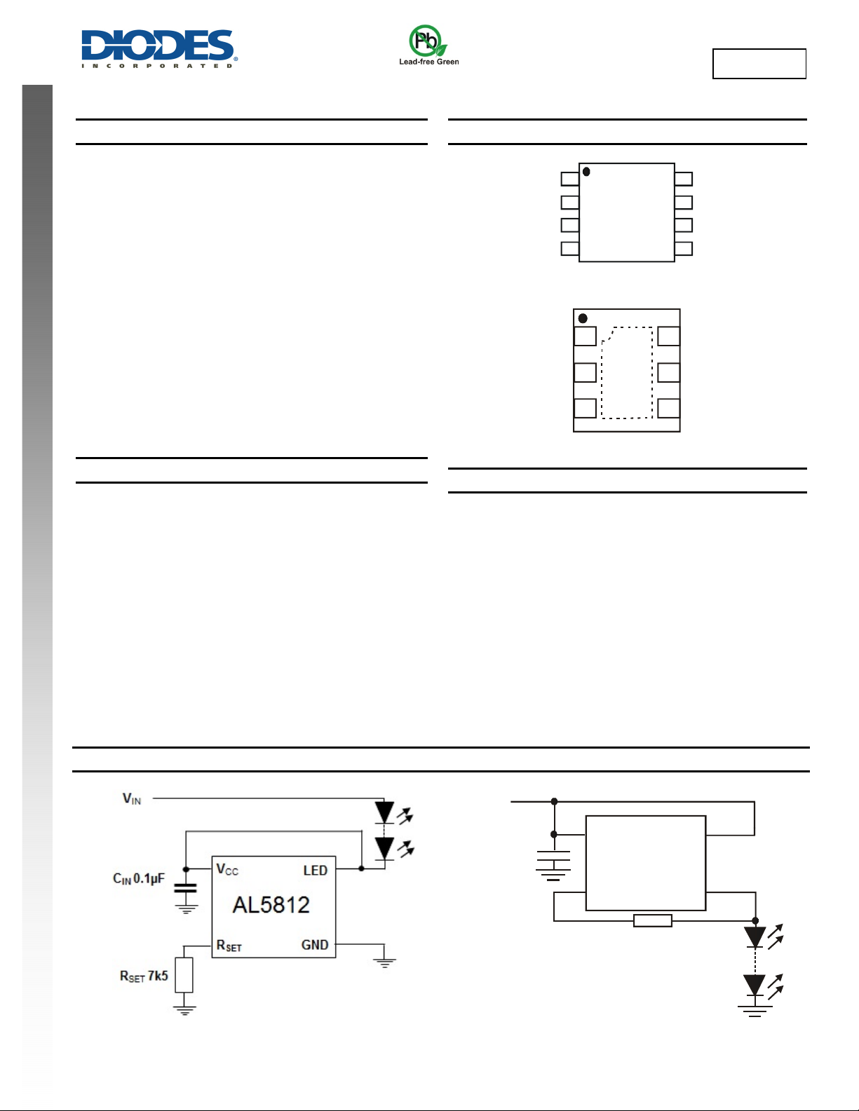
Pin Assignments
V
1
CC
2
NC
3
NC
4
SET
V
CC
1
NC
2
R
SET
3
Applications
• Isolated Offline LED Converters
• Linear LED Driver
• LED Signs
• Instrumentation Illumination
(Top View)
MSOP-8EP
(Top View)
Exposed
Pad
U-DFN3030-6
LED
8
NC
7
6
NC
5
GNDR
LED
6
NC
5
GND
4
L5812
Typical Applications Circuit
AL5812
Document number: DS35616 Rev. 2 - 2
C0.1µF
1 of 11
www.diodes.com
IN
IN
V
CC
LED
AL5812
R
SET
GND
R 7k5
SET
November 2013
© Diodes Incorporated
Page 2

A
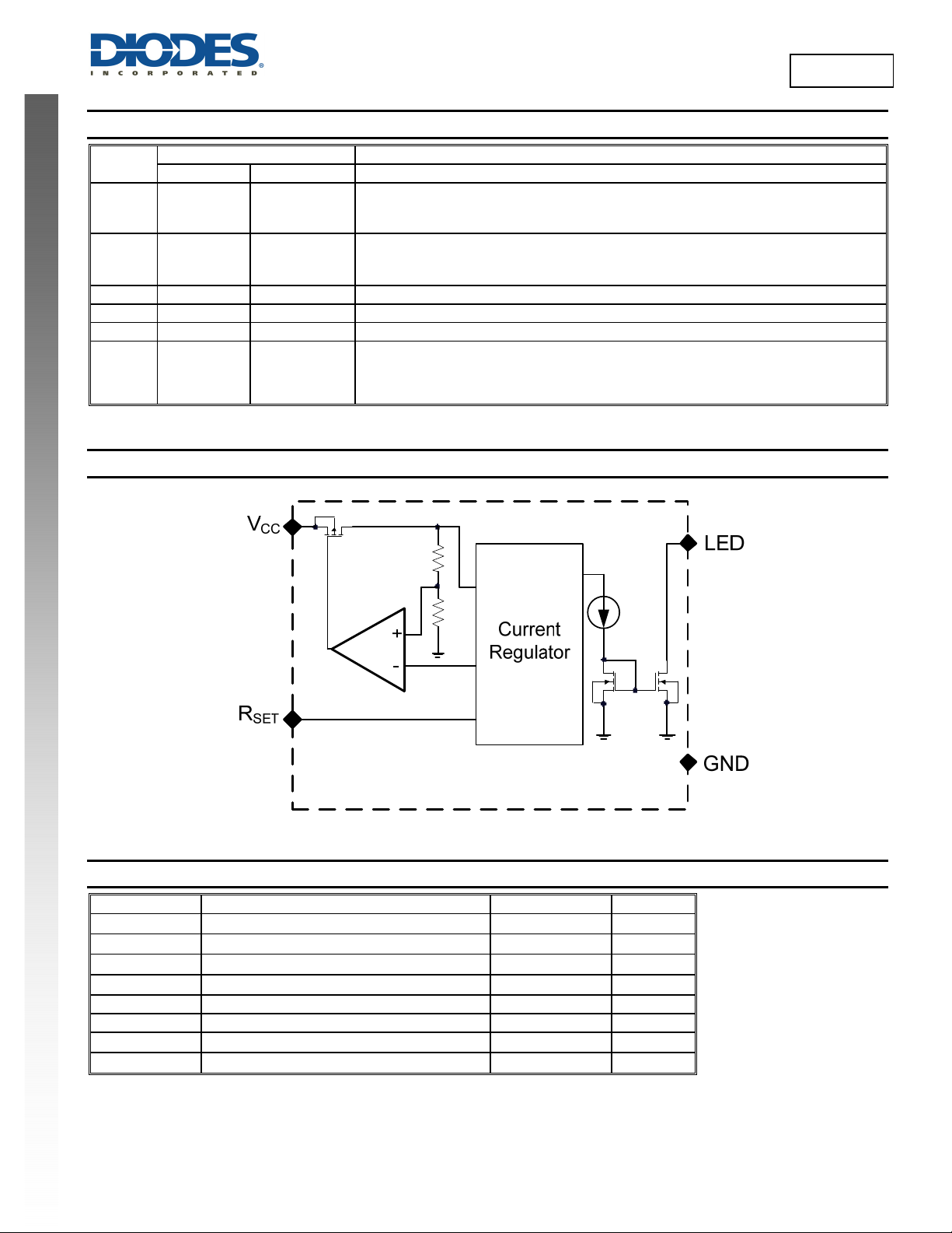
Pin Descriptions
L5812
Pin
Name
VCC
R
SET
GND 5 4 Ground Reference Point of Device.
LED 8 6 LED Current Sink Output.
NC 2, 3, 6, 7 2, 5 No Connection.
EP EP EP
Functional Block Diagram
NEW PRODUCT
(MSOP8-EP) (U-DFN3030-6)
Pin Number Function
1 1
4 3
Power Supply Input.
Connect a 0.1μF ceramic capacitor between V
device.
LED Current Setting Pin.
Connect a resistor from this pin to GND: I
May also be used to provide PWM dimming functionality.
Exposed Pad (bottom).
Used to improve thermal impedance of package.
It must be connected to GND directly underneath the package but not used as sole GND
potential terminal.
and GND as close as possible to the
CC
= 750/R
LED
SET
Absolute Maximum Ratings (@T
Symbol Parameters Ratings Unit
VCC
V
LED
V
R
RSET
I
LED
ESD HBM Human Body Model ESD Protection 1 kV
ESD CDM Charged Device Model ESD Protection 1.2 kV
TJ
TST
Note: 4.V
Caution: Stresses greater than the 'Absolute Maximum Ratings' specified above, may cause permanent damage to the device. These are stress ratings only;
functional operation of the device at these or any other conditions exceeding those indicated in this specification is not implied. Device reliability may be
affected by exposure to absolute maximum rating conditions for extended periods of time.
Semiconductor devices are ESD sensitive and may be damaged by exposure to ESD events. Suitable ESD precautions should be taken when
handling and transporting these devices.
CC
AL5812
Document number: DS35616 Rev. 2 - 2
Supply Voltage Relative to GND Pin (Note 4) -0.3 to +66 V
LED Pin Voltage Relative to GND Pin (Note 4) -0.3 to +66 V
Pin Voltage Relative to GND Pin
SET
LED Pin Current Sink Current Range 165 mA
Operating Junction Temperature -40 to +150 °C
Storage Temperature -55 to +150 °C
pin can be greater or smaller than V
= +25°C, unless otherwise specified.)
A
-0.3 to +6 V
; neither should go below GND.
LED
2 of 11
www.diodes.com
November 2013
© Diodes Incorporated
Page 3

A
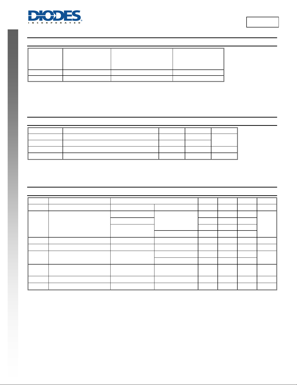
Package Thermal Data
θ
Package
Thermal Resistance
JC
Junction-to-Case
Thermal Resistance
Junction-to-Ambient
(Note 7)
MSOP-8EP 39 90°C/W (Note 5) 1.1W
U-DFN3030-6 14 69°C/W (Note 6) 1.47W
Notes: 5. Test condition for MSOP-8EP: Device mounted on FR-4 PCB (51mm x 51mm 2oz copper, minimum recommended pad layout on top layer and
thermal vias to bottom layer ground plane. For better thermal performance, larger copper pad for heat-sink is needed.
6. Test condition for U-DFN3030-6: Device mounted on FR-4 PCB (51mm x 51mm 2oz copper, minimum recommended pad layout on top layer and
thermal vias to bottom layer with maximum area ground plane. For better thermal performance, larger copper pad for heat-sink is needed
7. Dominant conduction path via exposed pad.
Recommended Operating Conditions (@T
Symbol Parameter Min Max Unit
VCC
V
NEW PRODUCT
I
LED
LED
TA
Notes: 8. For improved accuracy LED current should be greater than 60mA.
9. Maximum LED current is also limited by ambient temperature and power dissipation such that junction temperature should be kept less than or equal
to +125°C.
Electrical Characteristics (@T
Supply Voltage Range Relative to GND Pin
LED Pin Output Voltage Range Relative to GND Pin
LED Pin Current (Notes 8 & 9)
Operating Ambient Temperature Range
= +25°C, VCC= 3.5V, V
A
θ
JA
= +25°C, TJ = +125°C
T
A
(Note 7)
= +25°C, unless otherwise specified.)
A
P
DIS
(Note 7)
3.5 60
1 60
10 150 mA
-40 +125 °C
=1V (Note 10), R
LED
= 7.5kΩ unless otherwise specified.)
SET
V
L5812
Symbol Parameter Conditions Min Typ Max Unit
V
R
RSET
I
I
REG
LED
LINE
LED
LED Current Line Regulation
Voltage
SET
Current Accuracy
V
UVLO Under Voltage Lockout
ICC
I
LEAK
T
SHDN
T
HYS
Note: 10. All voltages unless otherwise stated are measured with respect to GND pin.
Supply Current
LED Pin Leakage Current
3.5V ≤ VCC ≤ 60V
V
R
SET
Thermal Shutdown 155
Thermal Shutdown Hysteresis 20
R
= 12.5kΩ
SET
R
= 4.99kΩ
SET
R
= 7.5kΩ
SET
= 3.5V to 60V TA = +25°C
CC
TA = -40°C to +125°C
TA = -40°C to +125°C
T
A
TA = -40°C to +125°C
= V
LED
= 60V
CC
= Open Circuit
= +25°C
T
A
= -40°C to +125°C
T
= +25°C
A
= +125°C
T
A
0.5 V
57 60 63
142.5 150 157.5
97 100 103
mA
95 105
0.25 %
2 V
320 400
500
µA
1 µA
°C
°C
AL5812
Document number: DS35616 Rev. 2 - 2
3 of 11
www.diodes.com
November 2013
© Diodes Incorporated
Page 4

A
ED CUR
REN
m
ED CURRENT (m
CUR
RENT
A
E
CURRENT
A
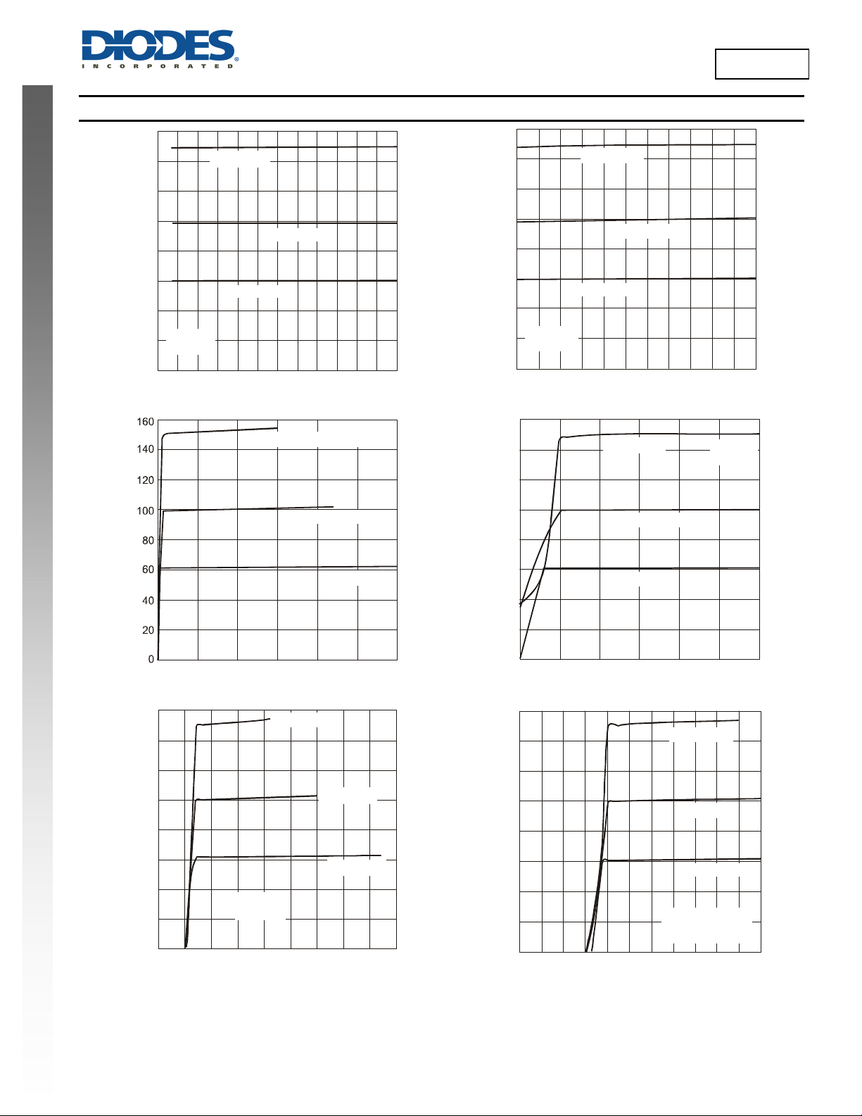
Typical Performance Characteristics
145
140
R = 4.99k
SET
Ω
160
140
R = 4.99k
SET
Ω
L5812
NEW PRODUCT
120
A)
100
T (
R = 7.5k
SET
Ω
80
60
L
40
V = 1.2V
LED
20
T = +25°C
A
0
0 5 10 15 20 25 30 35 40 45 50 55 60
R = 12.4k
SET
Ω
INPUT VOLTAGE (V)
Figure 1 LED Current vs. Input Voltage
R = 4.99k
LED CURRENT (mA)
SET
Ω
R = 7.5k
SET
R = 12.4k
SET
V = 3.5V
IN
T = +25°C
A
Ω
Ω
120
A)
100
R = 7.5k
Ω
SET
80
60
L
R = 12.4k
SET
Ω
40
V = 1.2V
LED
20
V = 3.5V
CC
0
-40 -25 -10 5
20 35 50 65 80 95 110 125
TEMPERATURE (°C)
Figure 2 LED Current vs. Ambie nt Temperature
160
)
(m
140
120
100
R = 4.99k
SET
Ω
R = 7.5k
SET
V = 3.5V
IN
T = +25°C
A
Ω
80
60
LED
R = 12.4k
SET
Ω
40
20
0 5 10 15 20 25 30
LED VOLTAGE (V)
Figure 3 LED Current vs. LED Pin Voltage (Note 11)
160
R = 4.99k
SET
Ω
140
120
R = 7.5k
100
SET
80
60
LED CURRENT (mA)
40
20
0
0 5 10 15 20 25 30 35 40 45
T = +25°C
A
2 LEDs
R = 12.4k
SET
INPUT VOLTAGE (V)
Figure 5 LED Current vs. Input Voltage - 2 LEDs
(Note 11 & 12)
Ω
Ω
0
0 0.5 1.0 1.5 2.0 2.5 3.0
LED VOLTAGE (V)
Figure 4 LED Current vs. LED Pin Voltage Zoomed
160
R = 4.99k
SET
R = 7.5k
SET
)
(m
140
120
100
80
60
D
L
R = 12.4k
SET
40
T = +25°C
20
0
0 2 4 6 8 10121416182022
A
V pin tied to LED pin
CC
2 LEDs
INPUT VOLTAGE (V)
Figure 6 LED Cur rent vs. Input Voltage
2 LEDs - High Side Drive (Notes 11, 12 &13)
Ω
Ω
Ω
Notes: 11. These curves have been limited at larger input voltages due to power dissipation.
12. Lower input voltage range is limited by the LED chain voltage
13. The AL5812 has its V
pin, which is connected to the anode of the LED chain. This creates a high side driver of the LED chain. See Figure 15.
pin connected to its LED pin, which are connected to the positive input supply voltage. R
CC
is connected to AL5812 GND
SET
AL5812
Document number: DS35616 Rev. 2 - 2
4 of 11
www.diodes.com
November 2013
© Diodes Incorporated
Page 5

A
C
URRENT
CUR
RENT
R VOLTAG
R VOLTAG
U
P
PLY C
U
R
RENT
UPP
Y CUR
R
N
T
Typical Performance Characteristics (cont.)
110
T = +25°C
A
100
2 LEDs
NEW PRODUCT
(mA)
LED
90
80
70
60
50
40
30
20
10
0
0.500
0.495
R = 7.5k
f = 100Hz
PWM
Ω
SET
10 200901008040 5030 7060
DUTY CYCLE (%)
Figure 7 LED Current vs. PWM Duty Cycle
V = 1.2V
LED
T = +25°C
A
L5812
14
V = 9V
IN
12
R = 75K
SET
Ω
10
(mA)
8
6
4
LED
2
0
-2
125 160130 155140 145 150135
TEMPERATURE (°C)
Figure 8 LED Current vs. T
0.500
0.495
T
SHDN
T
HYS
SHDN
V = 1.2V
LED
V = 3.5V
IN
0.490
E (V)
0.485
SET
R = 7.5k
SET
Ω
0.480
0.475
0 5 10 15 20 25 30 35 40 45 50 55 60
INPUT VOLTAGE (V)
Figure 9 R Voltage vs. Input Voltage
SET
400
350
R = 4.99k
SET
Ω
300
(µA)
250
R = 7.5k
SET
Ω
200
R = 12.4k
SET
Ω
150
S
100
V = 1.2V
LED
50
T = +25°C
A
0
0 5 10 15 20 25 30 35 40 45 50 55 60
INPUT VOLTAGE (V)
Figure 11 Supply Current vs. Input Voltage
E (V)
0.490
0.485
SET
0.480
0.475
-40 -25 -10 5 20 35 50 65 80 95 110 125
TEMPERATURE (C)
Figure 10 R Voltage vs. Ambient Temperature
SET
350
300
R = 4.99k
SET
250
(µA)
E
200
R = 12.4k
150
L
100
S
50
0
-40 -25 -10 5 20 35 50 65 80 95 110 125
SET
Ω
R = 7.5k
SET
Ω
Ω
V = 1.2V
LED
V = 3.5V
IN
TEMPERATURE (°C)
Figure 12 Supply Current vs. Ambient Temperature
R = 7.5k
SET
Ω
AL5812
Document number: DS35616 Rev. 2 - 2
5 of 11
www.diodes.com
November 2013
© Diodes Incorporated
Page 6

A
Application Information
Description
The AL5812 is a Linear LED driver and in normal operation has the LEDs connected to the same potential as its VCC pin and regulates the LED
current by sinking current into to its LED pin see Figure 13.
The LED current is set by the use of an external resistor, R
the AL5812 together with current regulator to set the LED current.
The nominal LED current is determined by this equation:
5.0
LED
SET
= 7.5k
LED
With R
The AL5812 with its 60V capability on its supply pin, V
drive LED chains up to 60V as shown in Figures 13 and 14. The voltage applied to the V
to the LED string. Figure 14 shows where you might control it from a 5-V rail but power the rails from a 12V rail.
*1500I =
*1500I
where 1500 is the current ratio between the LED pin current and R
R
SET
5.0
==
k5.7
mA100
, connected from the R
SET
, and its LED drive pin allows it to operate from supply rails up to 60V and/or directly
CC
pin to GND. This resistor supplies the bias current of
SET
pin current.
SET
pin can be greater or lower than the voltage applied
CC
V
LED
NEW PRODUCT
L5812
V
IN
V
CC
CIN0.1µF
Figure 13 Low Side Current LED Setting
Figure 14 Low Side Drive – Separate Supplies
R
R
SET
AL5812
SET
= 4.99kΩ
LED
GND
High Voltage Operation
An extension of Figure 14 is to derive the power for the AL5812 from the LED chain itself see Figure 15. LED chains greater than 60V can be
driven in this manner as long PWM dimming is not utilized.
V
IN
CIN0.1µF
V
CC
AL5812
R
SET
R
= 4.99kΩ
SET
LED
GND
Figure 15 shows the use of RC delay to match the power time delay between Vcc and LED pin. The AL5812 can also be used on the high side of
the LEDs, see Figure 16. This is a simple way of extending the maximum LED chain voltage, however, it does increase the minimum system input
voltage to:
V
Where
V
AL5812
Document number: DS35616 Rev. 2 - 2
Figure 15 Low Side LED String Tapping
= V
IN(min)
LED_CHAIN
LED_CHAIN
is the LED chain voltage.
+ 3.5V.
6 of 11
www.diodes.com
Figure 16 High Side Current LED String
November 2013
© Diodes Incorporated
Page 7

A
ED CURRENT (m
A
P
OWE
R
S
S
P
T
O
N
Application Information (cont.)
PWM Dimming
The AL5812 can be used to provide LED current dimming driving the R
switch to ground (Figure 17). The R
pin current is then effectively switched on and off causing the LED current to turn on and off. The linearity
SET
is shown in Figure 18.
NEW PRODUCT
Figure 17 PWM Dimming
Thermal Considerations
When designing linear LED drivers careful consideration must be given to:
1. the power dissipation within the LED driver
and
2. PCB layout/heat sinking.
A Linear LED driver has to be able to handle the large potential input voltage variations due to the supply voltage tolerance and also the variation
in LED forward voltage due to binning and temperature.
This can result in a large potential difference across the LED driver resulting in a larger than anticipated power dissipation.
For example in a 12V powered system with a 5% output voltage tolerance; the input voltage could typically vary from 12.6V down to 11.4V
driving 3 LEDs with a voltage varying from 3V to 3.5V at 100mA. This means that the LED driver has to cope with a voltage drop across varying
from approximately 3.6V to 0.9V. This means that the power dissipation of the AL5812 could be as much as 366mW.
Figure 19 below shows how the AL5812’s power dissipation capability varies with package; these values will vary with PCB size and area of
metal associated with the ground plane used for heat sinking. By increasing the area on the top layer the thermal impedance of both packages
could be improved.
1.6
pin via the current setting resistor (R
SET
110
T = +25°C
A
100
2 LEDs
Ω
R = 7.5k
SET
90
f = 500Hz
PWM
)
80
70
60
50
40
L
30
20
10
0
10 200901008040 5030 7060
DUTY CYCLE (%)
Figure 18 PWM Dimming Linearity
) and a series MOSFET
SET
L5812
1.4
1.2
(W)
I
1.0
A
I
0.8
DI
0.6
0.4
0.2
0.0
AL5812
Document number: DS35616 Rev. 2 - 2
U-DFN3030-6
MSOP-8EP
-40 -25 -10 5 20 35 50 65 80 95 110 125
AMBIENT TEMPERATURE (C)
Figure 19 Power Dissipation Deratin g
7 of 11
www.diodes.com
November 2013
© Diodes Incorporated
Page 8

A
Ordering Information
L5812
AL5812 XX - XX
Part Number Package Code Packaging
AL5812MP-13 MP MSOP-8EP 2500/Tape & Reel -13
AL5812FF-7 FF U-DFN3030-6 3000/Tape & Reel -7
Marking Information
(1) MSOP-8EP
NEW PRODUCT
(2) U-DFN3030-6
AL5812
Document number: DS35616 Rev. 2 - 2
Package
FF : U-D FN3030-6
MP : MSOP-8EP
Packing
7 : 7” Tape & Reel
13 : 13” Tape & Reel
Quantity Part Number Suffix
(Top View)
8 7 6 5
A~Z : Green
Logo
Y W X E
MSOP-8EP
Y : Year : 0~9
Part Number
AL5812
W : Week: A~Z : 1~26 week;
a~z : 27~52 week;
z represents 52 and 53 week
1 2 3 4
( Top View )
XX : Identification Code
Y
X X
W
XY
: Year : 0~9
: Week : A~Z : 1~26 week;
W
a~z : 27~52 week; z represents
52 and 53 week
: A~Z : Green
X
Part Number Package Identification Code
AL5812FF-7 U-DFN3030-6 B9
8 of 11
www.diodes.com
7”/13” Tape and Reel
November 2013
© Diodes Incorporated
Page 9

A
Package Outline Dimensions (All dimensions in mm.)
Please see AP02002 at http://www.diodes.com/datasheets/ap02002.pdf for latest version.
(1) MSOP-8EP
D
D1
E3
E1
Gauge Plane
Seating Plane
See Detail C
0.25
4
X
1
0
°
Detail C
c
NEW PRODUCT
x
y
1
e
A1
A
D
E
8Xb
A2
E2
A3
(2) U-DFN3030-6
AL5812
Document number: DS35616 Rev. 2 - 2
E
︵
Z︵4
A
Pin #1 ID
2
E
x
D
D
2
︶
45°︵0.35*0.35
e
︶
︶
b
A
1
A
3
Seating Plane
L
www.diodes.com
9 of 11
L5812
MSOP-8EP
Dim Min Max Typ
A - 1.10 -
4
X
1
0
°
a
L
A1 0.05 0.15 0.10
A2 0.75 0.95 0.86
A3 0.29 0.49 0.39
b 0.22 0.38 0.30
c 0.08 0.23 0.15
D 2.90 3.10 3.00
D1 1.60 2.00 1.80
E 4.70 5.10 4.90
E1 2.90 3.10 3.00
E2 1.30 1.70 1.50
E3 2.85 3.05 2.95
e - - 0.65
L 0.40 0.80 0.60
a 0° 8° 4°
x - - 0.750
y - - 0.750
All Dimensions in mm
U-DFN3030-6
Dim Min Max Typ
A 0.57 0.63 0.60
A1 0 0.05 0.02
A3 - - 0.15
b 0.35 0.45 0.40
D 2.95 3.05 3.00
D2 2.25 2.45 2.35
E 2.95 3.05 3.00
E2 1.48 1.68 1.58
e - - 0.95
L 0.35 0.45 0.40
Z - - 0.35
All Dimensions in mm
November 2013
© Diodes Incorporated
Page 10

A
Suggested Pad Layout
Please see AP02001 at http://www.diodes.com/datasheets/ap02001.pdf for latest version.
(1) MSOP-8EP
X C
G
Y
Y2
X1
Y1
NEW PRODUCT
(2) U-DFN3030-6
X
2
X
1
C
C-0.409
AL5812
Document number: DS35616 Rev. 2 - 2
X
Y
1
Y
2
Y
www.diodes.com
10 of 11
Dimensions
C 0.650
G 0.450
X 0.450
X1 2.000
Y 1.350
Y1 1.700
Y2 5.300
Dimensions
C 0.950
X 0.500
X1 2.400
X2 2.550
Y 0.600
Y1 1.780
Y2 3.300
Value
(in mm)
Value
(in mm)
L5812
November 2013
© Diodes Incorporated
Page 11

A
DIODES INCORPORATED MAKES NO WARRANTY OF ANY KIND, EXPRESS OR IMPLIED, WITH REGARDS TO THIS DOCUMENT,
INCLUDING, BUT NOT LIMITED TO, THE IMPLIED WARRANTIES OF MERCHANTABILITY AND FITNESS FOR A PARTICULAR PURPOSE
(AND THEIR EQUIVALENTS UNDER THE LAWS OF ANY JURISDICTION).
Diodes Incorporated and its subsidiaries reserve the right to make modifications, enhancements, improvements, corrections or other changes
without further notice to this document and any product described herein. Diodes Incorporated does not assume any liability arising out of the
application or use of this document or any product described herein; neither does Diodes Incorporated convey any license under its patent or
trademark rights, nor the rights of others. Any Customer or user of this document or products described herein in such applications shall assume
all risks of such use and will agree to hold Diodes Incorporated and all the companies whose products are represented on Diodes Incorporated
website, harmless against all damages.
Diodes Incorporated does not warrant or accept any liability whatsoever in respect of any products purchased through unauthorized sales channel.
Should Customers purchase or use Diodes Incorporated products for any unintended or unauthorized application, Customers shall indemnify and
hold Diodes Incorporated and its representatives harmless against all claims, damages, expenses, and attorney fees arising out of, directly or
indirectly, any claim of personal injury or death associated with such unintended or unauthorized application.
Products described herein may be covered by one or more United States, international or foreign patents pending. Product names and markings
noted herein may also be covered by one or more United States, international or foreign trademarks.
This document is written in English but may be translated into multiple languages for reference. Only the English version of this document is the
final and determinative format released by Diodes Incorporated.
NEW PRODUCT
Diodes Incorporated products are specifically not authorized for use as critical components in life support devices or systems without the express
written approval of the Chief Executive Officer of Diodes Incorporated. As used herein:
A. Life support devices or systems are devices or systems which:
1. are intended to implant into the body, or
labeling can be reasonably expected to result in significant injury to the user.
B. A critical component is any component in a life support device or system whose failure to perform can be reasonably expected to cause the
failure of the life support device or to affect its safety or effectiveness.
Customers represent that they have all necessary expertise in the safety and regulatory ramifications of their life support devices or systems, and
acknowledge and agree that they are solely responsible for all legal, regulatory and safety-related requirements concerning their products and any
use of Diodes Incorporated products in such safety-critical, life support devices or systems, notwithstanding any devices- or systems-related
information or support that may be provided by Diodes Incorporated. Further, Customers must fully indemnify Diodes Incorporated and its
representatives against any damages arising out of the use of Diodes Incorporated products in such safety-critical, life support devices or systems.
Copyright © 2013, Diodes Incorporated
www.diodes.com
2. support or sustain life and whose failure to perform when properly used in accordance with instructions for use provided in the
IMPORTANT NOTICE
LIFE SUPPORT
L5812
AL5812
Document number: DS35616 Rev. 2 - 2
11 of 11
www.diodes.com
November 2013
© Diodes Incorporated
 Loading...