Diodes AL5801W6 Schematic [ru]

A
L5801
100V, ADJUSTABLE CURRENT SINK LINEAR LED DRIVER
EXT
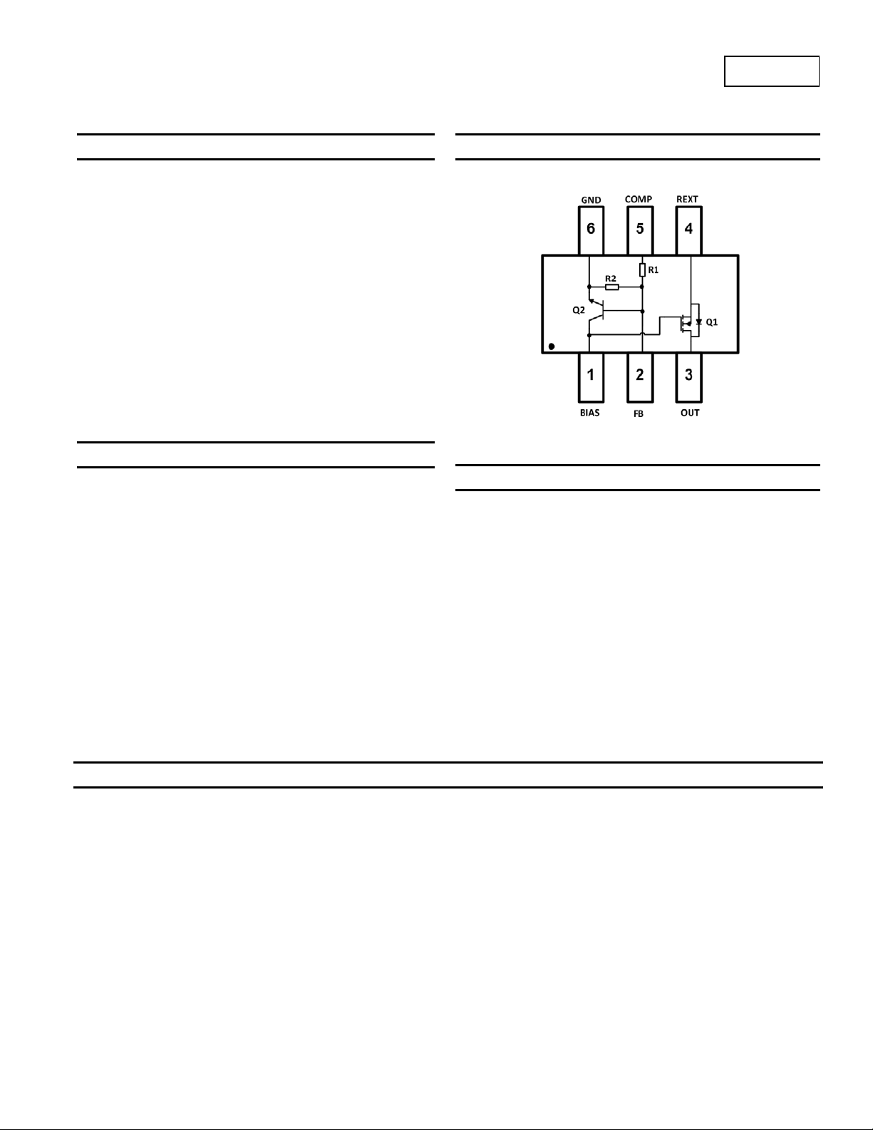
Pin Assignments
Applications
• Linear LED Drivers
• LED Signs
• Offline LED Luminaries
(Top View)
SOT26
Description
The AL5801 combines a 100V N-channel MOSFET with a prebiased NPN transistor to make a simple, small footprint LED driver.
The LED current is set by an external resistor connected from R
pin (4) to GND pin (6). The internal pre-biased transistor develops
approximately 0.56V across the external resistor.
The AL5801 open-drain output can operate from 1.1V to 100V
enabling it to operate 5V to 100V power supplies without additional
components.
PWM dimming of the LED current can be achieved by driving the
BIAS pin (1) with an external, open-collector NPN transistor or
open-drain N-channel MOSFET.
The AL5801 is available in a SOT26 package and is ideal for driving
LED currents up to 350mA.
Features
• Feedback Pin Reference Voltage V
• -40°C to +125°C Temperature Range
• 1.1V to 100V Open-Drain Output
• Negative temperature V
the LED current at high temperatures
• Low thermal impedance SOT26 package with copper lead
frame
• Lead-Free Finish; RoHS Compliant (Notes 1 & 2)
• Halogen and Antimony Free. “Green” Device (Note 3)
• Qualified to AEC-Q101 Standards for High Reliability
Notes: 1. EU Directive 2002/95/EC (RoHS) & 2011/65/EU (RoHS 2) compliant. All applicable RoHS exemptions applied.
2. See http://www.diodes.com for more information about Diodes Incorporated’s definitions of Halogen- and Antimony-free, "Green" and Lead-free.
3. Halogen- and Antimony-free "Green” products are defined as those which contain <900ppm bromine, <900ppm chlorine (<1500ppm total Br + Cl)
and <1000ppm antimony compounds.
co-efficient automatically reduces
RSET
= 0.56V at +25°C
RSET
Typical Applications Circuit
AL5801
Document number: DS35555 Rev. 3 - 2
1 of 11
www.diodes.com
July 2012
© Diodes Incorporated

A
Pin Descriptions
Pin
Number
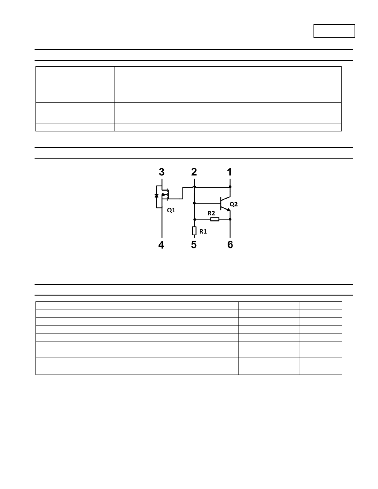
1 BIAS Biases the open-Drain output MOSFET
2 FB Feedback pin
3 OUT Open-Drain LED driver output
4 R
5 COMP
6 GND Ground refe rence point for setting the LED current
Pin
Name
Current sense pin. LED current sensing resistor should be connected from here to GND
EXT
Compensation pin. Connect COMP pin to REXT pin and insert a 1nF ceramic capacitor from COMP
pin to FB pin for improved transient stability
Functional Block Diagram
L5801
Function
Figure 1 Block Diagram
Absolute Maximum Ratings (@T
Symbol Characteristics Values Unit
V
OUT
V
BIAS
VFB
V
COMP
V
REXT
I
OUT
TJ
TST
Note: 4. With pins 5 and 6 connected together.
These are stress ratings only. Operation outside the absolute maximum ratings may cause device failure.
Operation at the absolute maximum rating for extended periods may reduce device reliability.
Output voltage relative to GND 100 V
BIAS voltage relative to GND (Note 4) 20 V
FB voltage relative to GND 6 V
COMP voltage relative to GND 6 V
REXT voltage relative to GND 6 V
Output current 350 mA
Operating junction temperature -40 to +150 °C
Storage temperature -55 to +150 °C
= +25°C, unless otherwise specified.)
A
AL5801
Document number: DS35555 Rev. 3 - 2
2 of 11
www.diodes.com
July 2012
© Diodes Incorporated

A
L5801
Package Thermal Data
Characteristic Symbol Value Unit
Power Dissipation (Note 5) @ TA = +25°C
Power Dissipation (Note 6) @ TA = +25°C
Power Dissipation (Note 7) @ TA = +25°C
Power Dissipation (Note 8) @ TA = +25°C
Thermal Resistance, Junction to Ambient Air (Note 5) @ TA = +25°C
Thermal Resistance, Junction to Ambient Air (Note 6) @ TA = +25°C
Thermal Resistance, Junction to Ambient Air (Note 7) @ TA = +25°C
Thermal Resistance, Junction to Ambient Air (Note 8) @ TA = +25°C
Notes: 5. Device mounted on 15mm x 15mm 2oz copper board.
6. Device mounted on 25mm x 25mm 1oz copper board.
7. Device mounted on 25mm x 25mm 2oz copper board.
8. Device mounted on 50mm x 50mm 2oz copper board.
P
D
R
JA
θ
0.75
0.70
0.85
1.05
165
180
145
120
W
°C/W
Recommended Operating Conditions (@T
= +25°C, unless otherwise specified.)
A
Symbol Parameter Min Max Unit
V
BIAS
V
OUT
I
LED
TA
Note: 9. Subject to ambient temperature, power dissipation and PCB.
NMOSFET Electrical Characteristics: (Q1) (@T
OFF CHARACTERISTICS
Drain-Source Breakdown Voltage
Zero Gate Voltage Drain Current
Gate-Source Leakage
ON CHARACTERISTICS
Gate Threshold Voltage
Static Drain-Source On-Resistance
Forward Transconductance
Diode Forward Voltage
DYNAMIC CHARACTERISTICS
Input Capacitance
Output Capacitance
Reverse Transfer Capacitance
AL5801
Document number: DS35555 Rev. 3 - 2
Supply voltage range 3.5 20
OUT voltage range 1.1 100
V
LED pin current (Note 9) 25 350 mA
Operating ambient temperature range -40 125 °C
= +25°C, unless otherwise specified.)
A
Characteristic Symbol Min Typ Max Unit Test Condition
BV
DSS
I
DSS
I
⎯ ⎯
GSS
V
GS(th)
R
⎯
DS (ON)
g
⎯
fs
V
SD
C
⎯
iss
C
⎯
oss
C
rss
100
⎯ ⎯
2.0
⎯
0.89 1.1 V
⎯
⎯ ⎯
±100
⎯
⎯
⎯
0.85
0.99
0.9
129
14
8
1 µA
4.1 V
⎯
⎯
⎯
⎯
V
V
GS
V
DS
nA
V
GS
V
DS
V
GS
Ω
V
GS
S
V
DS
VGS = 0V, IS = 1.5A
pF
V
pF
pF
DS
f = 1.0MHz
= 0V, ID = 250µA
= 60V, VGS = 0V
= ±20V, VDS = 0V
= VGS, ID = 250µA
= 10V, ID = 1.5A
= 6V, ID = 1A
= 15V, ID = 1A
= 50V, VGS = 0V
3 of 11
www.diodes.com
July 2012
© Diodes Incorporated

A
M
A
P
OWER D
PATIO
N
M
P
OWER D
PATIO
N
U
NCTIO
N T
O
N
T
R
Pre-Bias Transistor Electrical Characteristics: (Q2) (@T
Characteristic (Note 10) Symbol Min Typ Max Unit Test Condition
V
Input Voltage
Output Voltage
Output Current
DC Current Gain
Input Resistance
Resistance Ratio
Notes: 10. Short duration pulse test used to minimize self-heating effect.
V
V
I
R
I(off)
I(on)
O(on)
O(off)
G
R
1
2/R1
1
0.4 - - V
- - 1.5 V
- 0.05 0.3 V
- - 0.5
80 - - -
3.2 4.7 6.2 kΩ 8 10 12 - -
Thermal Characteristics
1.2
1.2
= +25°C, unless otherwise specified.)
A
VCC = 5V, IO = 100μA
VCC = 0.3V, IO = 5mA
IO/II = 5mA/0.25mA
μA
VCC = 50V, VI = 0V
VO = 5V, IO = 10mA
L5801
1.0
(W)
ISSI
0.8
0.6
50mm x 50mm
(2oz. FR4)
25mm x 25mm
(2oz. FR4)
15mm x 15mm
(2oz. FR4)
0.4
X
0.2
0
0 25 50 75 100 125 150
TEMPERATURE (°C)
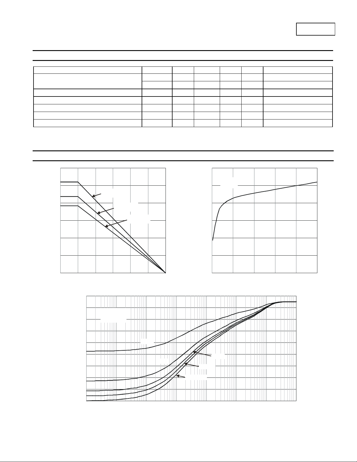
Figur e 2 Derating Cur ve
180
160
140
T = 25°C
A
25mm x 25mm
1oz. FR4
AI
120
100
AMBIE
D = 0.5
80
60
D = 0.2
T = 25°C
A
2oz. FR4
1.0
(W)
0.8
ISSI
0.6
0.4
AX
0.2
0
0 500 1,000 1,500 2,000 2,500
COPPER AREA (mm )
D = 0.1
D = 0.05
Figur e 3 Area vs. Max Power
2
J
40
THERMAL RESISTANCE (°C/W)
Single Pulse
20
0
0.0001 0.001 0.01 0.1 1 10 100 1,000
PULSE WIDTH (s)
Figure 4 Tran si ent Therm al Impedance
AL5801
Document number: DS35555 Rev. 3 - 2
4 of 11
www.diodes.com
July 2012
© Diodes Incorporated
 Loading...