

Page 1
AL3159
HIGH EFFICIENCY 1x/2x CHARGE PUMP
FOR WHITE LED APPLICATIONS
Description
The AL3159 is a low noise, constant frequency charge pump
DC/DC converter that uses a Dual mode load switch (1x), and (2x)
conversion for white LED applications. The AL3159 is capable of
driving nine LED channels at 20mA from a 2.7V to 5.5V input. The
current sinks may be operated using three simple logic control
inputs individually or in parallel for driving higher-current LEDs. Low
external part counts (one 1µF flying capacitor and two
2.2µF capacitors at V
small, battery-powered applications.
AL3159 digital inputs are used to enable or disable the
LED channels with a fixed default current settings at 20mA or other
factory programming options available.
Each output of the AL3159 is equipped with built-in protection for
V
short circuit and auto-disable for LED short conditions. Built-in
OUT
soft-start circuitry prevents excessive inrush current during start-up
and mode switching. A low-current shutdown feature disconnects
the load from V
The AL3159 is available in a lead-free, space-saving, thermally
enhanced 20-pin 3 x 3mm QFN package.
Features
NEW PRODUCT
• V
range: 2.7V to 5.5V
IN
• Up to 93% Max Power Efficiency
• 1% Current Matching Accuracy Between Channels
• Drives up to 9 configurable Channels of LEDs
• Three simple logic decoding LED On/Off control inputs
• Low transition threshold voltage typical 150 mV
• Dual-Mode 1x and 2x Charge Pump
• 1.2 MHz Constant Switching Frequency
• V
• Soft Start for reducing inrush current
• I
• Thermally-Enhanced QFN3030-20 Package: Available in
• Lead Free Finish/ RoHS Compliant (Note 1)
Notes: 1. EU Directive 2002/95/EC (RoHS). All applicable RoHS exemptions applied. Please visit our website at
short circuit and Thermal Protections
OUT
<1µA in Shutdown
Q
“Green” Molding Compound (No Br, Sb)
http://www.diodes.com/products/lead_free.html
and V
IN
to reduce quiescent current less than 1µA.
IN
) make this part ideally suited for
OUT
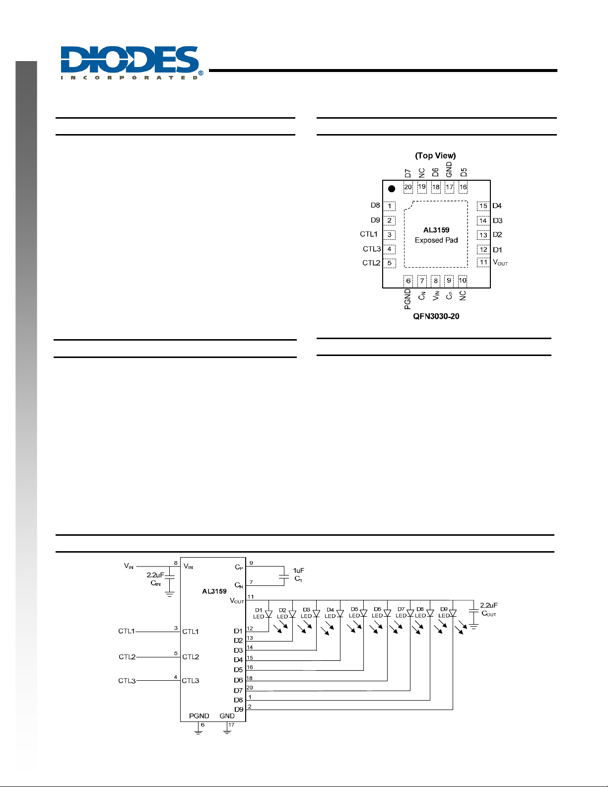
Pin Assignments
Applications
• Mobile Phone White LED Backlighting and Indicators
• PDA White LED backlighting
• Battery-operated Phone Main and Sub Screen White LED
Backlighting
Typical Application Circuit
AL3159
Document number: DS35048 Rev. 2 - 2
1 of 10
www.diodes.com
January 2011
© Diodes Incorporated
Page 2
Pin Descriptions
Pin Name Pin Number Description
D8 1 Current sink input #8. Connected to V
D9 2 Current sink input #9. Connected to V
CTL1 3 Control Pin 1
CTL3 4 Control Pin 3
CTL2 5 Control Pin 2
PGND 6 Charge Pump Switch Ground
CN 7 Negative Terminal of Flying Capacitor
VIN 8 Input Power Supply. Requires 2.2µF capacitor between this pin and ground.
CP 9 Positive Terminal of Flying Capacitor
NC 10,19 No-Connect
V
OUT
D1 12 Current sink input #1. Connected to V
D2 13 Current sink input #2. Connected to V
D3 14 Current sink input #3. Connected to V
D4 15 Current sink input #4. Connected to V
NEW PRODUCT
D5 16 Current sink input #5. Connected to V
GND 17 Ground
D6 18 Current sink input #6. Connected to V
D7 20 Current sink input #7. Connected to V
GND EP PAD Exposed Pad (bottom). Connected to GND directly underneath the package.
11
Charge pump output to drive load circuit. Requires 2.2µF capacitor between this pin
and ground.
AL3159
HIGH EFFICIENCY 1x/2x CHARGE PUMP
FOR WHITE LED APPLICATIONS
when un-used.
OUT
when un-used.
OUT
when un-used.
OUT
when un-used.
OUT
when un-used.
OUT
when un-used.
OUT
when un-used.
OUT
when un-used.
OUT
when un-used.
OUT
Functional Block Diagram
AL3159
Document number: DS35048 Rev. 2 - 2
2 of 10
www.diodes.com
January 2011
© Diodes Incorporated
Page 3
HIGH EFFICIENCY 1x/2x CHARGE PUMP
FOR WHITE LED APPLICATIONS
Absolute Maximum Ratings (Note 2)
Symbol Description Rating Unit
ESD HBM Human Body Model ESD Protection 2 KV
ESD MM Machine Model ESD Protection 200 V
VIN Input Voltage -0.3 to 6 V
V
Notes: 2. Exceeding Absolute Maximum Ratings will cause permanent damage to the device.
Recommended Operating Conditions
Symbol Parameter Min Max Unit
NEW PRODUCT
Electrical Characteristics (T
Symbol Parameter Test Conditions Min Typ. Max Unit
I
SHDN
I
D-Match
R
VTH
VHS Mode Transition Hysteresis 250 mV
TSS Soft-Start Time 100 µs
Fsw Switching Frequency 1.2 MHz
V
CTL1, 2,3 (L)
V
CTL1,2,3(H)
T
CTL1,2,3
UVLO VIN Under-Voltage Lockout 1.8 2 2.2 V
I
CTL1,2,3
T
T
Notes: 3. Determined by the average current levels of all active channels
4. Defined as the deviation of any sink current from the average of all active current channels.
5. Device mounted on FR-4 substrate, 2"*2", 2oz copper, double-sided PC board, with minimum recommended pad on top layer and
4 vias to bottom layer.
CTL1, CTL2, CTL3 to GND Voltage -0.3 to VIN +0.3 V
CTL1,2,3
I
Maximum DC Output Current 270 mA
OUT
TJ Operating Junction Temperature Range 150
T
Maximum Soldering Temperature (at leads, 10 sec) 300
LEAD
VIN Input Voltage 2.7 5.5 V
TA Operating Amb ient Temperature -40 85 °C
= 25°C, V
A
IQ Quiescent Current
= 3.6V, CIN = C
IN
= 2.2µF, C1 = 1µF Unless otherwise noted)
OUT
1x Mode, 3.0≤VIN≤5.5, Active,
No Load Current
2x Mode, 3.0≤VIN≤5.5, Active,
No Load Current
0.3 0.6
2 5
Shutdown Current CTL1, CTL2 and CTL3 = 0 1 µA
I
IDX
Open Loop V
out
Current Accuracy (Note 3)
SINK
Current Matching Between Any Two
Current Sink Inputs (Note 4)
Resistance
OUT
1x to 2x Transition Threshold at Any
Pin
I
SINK
19 20 21 mA
VF: D1:D9 = 3.6V 1 2 %
1x mode 0.5
2 x mode 4.5
= 20mA 150 mV
I
DX
CTL1,2,3 Threshold Low VIN = 2.7V 0.4 V
CTL1,2,3 Threshold High VIN = 5.5V 1.4 V
CTL1,2,3 Off Timeout 200 µs
CTL1,2,3 Input Leakage -1 1 µA
SHDN
HYS
θ
JA
Thermal shutdown Protection 160
Thermal shutdown hysteresis 10
Thermal Resistance Junction-to-
Ambient
QFN3030-20 (Note 5)
48
AL3159
°C
°C
mA
Ω
°C
°C
o
C/W
AL3159
Document number: DS35048 Rev. 2 - 2
3 of 10
www.diodes.com
January 2011
© Diodes Incorporated
Page 4

Typical Performance Characteristics
Turn-On to 1x Mode
AL3159
HIGH EFFICIENCY 1x/2x CHARGE PUMP
FOR WHITE LED APPLICATIONS
Turn-On to 2x Mode
NEW PRODUCT
CTL1,2,3
2V/div
Vout
2V/div
Cp
2V/div
Iin
200mA/div
50us/div
Turn-Off from 1x Mode
VIN=4.2V
T
=25°C
A
I
=20mA
L
VIN=4.2V
T
=25°C
A
=20mA
I
L
CTL1,2,3
2V/div
Vout
2V/div
Cp
2V/div
Iin
200mA/div
CTL1,2,3
2V/div
Vout
2V/div
Cp
2V/div
Iin
200mA/div
100us/div
Turn-Off from 2x Mode
VIN=3.0V
=25°C
T
A
I
=20mA
L
VIN=3.0V
T
=25°C
A
I
=20mA
L
CTL1,2,3
2V/div
Vout
2V/div
Cp
2V/div
Iin
200mA/div
200ms/div
Load Characteristics in 2x Mode
1us/div
AL3159
Document number: DS35048 Rev. 2 - 2
200ms/div
Load Characteristics in 2x Mode
Vin
200mV
AC/div
Vout
200mVAC/div
Iin
100mA/div
January 2011
© Diodes Incorporated
VIN=2.7V
T
=25°C
A
I
=20mA
L
Vin
200mVAC/div
Vout
200mV
AC/div
Iin
AC/div
100mA
4 of 10
www.diodes.com
VIN=3.0V
T
=25°C
A
I
=20mA
L
1us/div
Page 5

HIGH EFFICIENCY 1x/2x CHARGE PUMP
Typical Performance Characteristics (Continued)
AL3159
FOR WHITE LED APPLICATIONS
NEW PRODUCT
VF=3.1V
=25°C
T
A
I
=20mA
L
Channels 1 to 9
=3.6V
V
IN
Channels 1 to 9
V
TA=25°C
=3.6 V
IN
AL3159
Document number: DS35048 Rev. 2 - 2
V
CTL(H)
V
CTL(L)
VIN=2.7V VIN=3.6V
5 of 10
www.diodes.com
January 2011
© Diodes Incorporated
Page 6

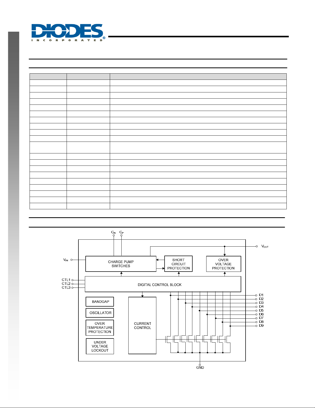
Functional Description
The AL3159 is a dual-mode high efficiency charge pum p
(1x and 2x) device, driving nine LED channels with three
simple logic control inputs, intended for white
LED backlight applications. An internal comparator circui t
compares the voltage at each constant current sink input
against a reference voltage. To ensure maximum po wer
efficiency, the most appropriate switching mode (1x and
2x) is automatically selected.
The AL3159 requires only three external components: one
1 µF ceramic flying capacitor (C1) for the charge pump,
one 2.2µF ceramic input capacitor (C
2.2µF ceramic charge pump output capacitor (C
The each output channel of the AL3159 can drive nine
individual LEDs with a maximum current of fixed
manufacture setting (20mA or 30mA) per channel. These
can be paralleled to give a total maximum output current of
270mA.
NEW PRODUCT
CTL<3:1> LED ON/OFF CONT ROL
000 ALL OFF
001 LED1~LED2 ON
010 LED3~LED5 ON
011 LED6~LED9 ON
100 LED9 ON
101 LED6~LED8 ON
110 LED1~LED5 ON
111 ALL ON
IN
), and one
).
OUT
AL3159
HIGH EFFICIENCY 1x/2x CHARGE PUMP
FOR WHITE LED APPLICATIONS
Disabled Current Sinks
Unused current channels must be disabled by connecting
the sinks to VOUT with only a small sense current flowing
through the disabled channel.
Soft-Start
Soft-start is incorporated to prevent excessive inrush
current during power-up, mode switching, and
transitioning out of stand-by mode.
Short-Circuit Protection
Short-circuit protection function is incorporated to prevent
excessive load current when either flying cap terminals or
output pin electrically tied to a very lower voltage or
ground.
Over-Voltage Protection
Over-Voltage Protection function is incorporated to limit
the output voltage under a safe value to avoid on-chip
device breakdown.
Under-Voltage Lockout
Under-Voltage lockout feature disables the device when
the input voltage drops below UVLO threshold.
Thermal Auto Shutdown
When the die temperature exceeds the thermal limit, the
device will be disabled and enter stand-by mode. The
operation resumes whenever the die cools off sufficiently.
AL3159
Document number: DS35048 Rev. 2 - 2
6 of 10
www.diodes.com
January 2011
© Diodes Incorporated
Page 7

Ordering Information
AL3159
HIGH EFFICIENCY 1x/2x CHARGE PUMP
FOR WHITE LED APPLICATIONS
AL 3159 FS G - 7
Package
FS : QFN3030-20
Green
G : Green
Packing
7 : Tape & Reel
Device
AL3159FSG-7 FS QFN3030-20 3000/Tape & Reel -7
Notes: 7. Pad layout as shown on Diodes Inc. suggested pad layout document AP02001, which can be found on our website at
http://www.diodes.com/datasheets/ap02001.pdf
8. EU Directive 2002/95/EC (RoHS). All applicable RoHS exemptions applied. Please visit our website at
http://www.diodes.com/products/lead_free.html
NEW PRODUCT
Marking Information
(1) QFN3030-20
Package
Code
Packaging
(Note 7 and 8)
Quantity Part Number Suffix
7” Tape and Reel
(Top View)
: B9 : AL3159
XX
: Year : 0~9
X X
W
XY
Y
: Week : A~Z : 1~26 week;
W
a~z : 27~52 week; z represents
52 and 53 week
: A~Z : Green
X
Part Number Package Identification Code
AL3159FSG QFN3030-20 B9
AL3159
Document number: DS35048 Rev. 2 - 2
7 of 10
www.diodes.com
January 2011
© Diodes Incorporated
Page 8

Package Outline Dimensions (All Dimensions in mm)
Package type: QFN3030-20
CL
Side View
2.95/3.05
10
1.70/1.90
20
0.16/0.26
0.595 Typ.
Bottom View
0.15 Typ.
A
1.70/1.90
0.30/0.40
15
NEW PRODUCT
0.10 C
0.08 C Seating Plane
0.05 Max.
0.57/0.63
B
0.25 A
2X-
5
Pad Layout Top View
2X-
2.95/3.05
Pin1
(Pin #1 ID)
0.25 B
0.40
C
0.10
AL3159
HIGH EFFICIENCY 1x/2x CHARGE PUMP
FOR WHITE LED APPLICATIONS
C
AB
AL3159
Document number: DS35048 Rev. 2 - 2
8 of 10
www.diodes.com
January 2011
© Diodes Incorporated
Page 9

Taping Orientation (Note 9)
AL3159
HIGH EFFICIENCY 1x/2x CHARGE PUMP
FOR WHITE LED APPLICATIONS
NEW PRODUCT
Notes: 9. The taping orientation of the other package type can be found on our website at http://www.diodes.com/datasheets/ap02007.pdf
AL3159
Document number: DS35048 Rev. 2 - 2
9 of 10
www.diodes.com
January 2011
© Diodes Incorporated
Page 10

AL3159
HIGH EFFICIENCY 1x/2x CHARGE PUMP
FOR WHITE LED APPLICATIONS
NEW PRODUCT
IMPORTANT NOTICE
DIODES INCORPORATED MAKES NO WARRANTY OF ANY KIND, EXPRESS OR IMPLIED, WITH REGARDS TO THIS
DOCUMENT, INCLUDING, BUT NOT LIMITED TO, THE IMPLIED WARRANTIES OF MERCHANTABILITY A ND FITNESS FOR A
PARTICULAR PURPOSE (AND THEIR EQUIVALENTS UNDER THE LAWS OF ANY JURISDICTION).
Diodes Incorporated and its subsidiaries reserve the right to make modifications, enhancements, improvements, corrections or other
changes without further notice to this document and any product described herein. Diodes Incorporat ed does not assume any liability
arising out of the application or use of this document or any product described herein; neither does Diodes Incorporated convey any
license under its patent or trademark rights, nor the rights of others. A ny Customer or user of this document or products described
herein in such applications shall assume all risks of such use and will agree to hold Diodes Incorporated and all the companies
whose products are represented on Diodes Incorporated website, harml ess ag ai nst all damages.
Diodes Incorporated does not warrant or acc ept any liability whatsoever in respec t of any products purchas ed through unauthorized
sales channel.
Should Customers purchase or use Diodes Incorporated products for any unintended or unauthorized application, Customers shall
indemnify and hold Diodes Incorporated and its representatives harmless agai nst all claims, damages, expenses, and attorney fees
arising out of, directly or indirectly, any claim of personal injury or death ass ociated with such unintended or unauthorized application.
Products described herein may be covered by one or more United Stat es, international or foreign patents pending. Product names
and markings noted herein may also be covered by one or more United States, international or foreign trademarks.
LIFE SUPPORT
Diodes Incorporated products are specifically not authorized for use as critical components in life support devices or systems without
the express written approval of the Chief Executive Officer of Diodes Incorporated. As used herei n:
A. Life support devices or systems are devices or systems which:
1. are intended to implant into the body, or
2. support or sustain life and whose failure to perform when properly used in accordance with instructi ons for us e provided
in the labeling can be reasonably expected to result in significant injury to the user.
B. A critical component is any component in a life support device or system whose failure to perform can be reasonably expected
to cause the failure of the life support device or to affect its safety or effectiveness .
Customers represent that they have all necessary expertise in the safety and regulatory ramifications of their life support devices or
systems, and acknowledge and agree that they are solely responsible for all legal, regulatory and safety-related requirements
concerning their products and any use of Diodes Incorporated products in such safety-critical, life support devices or systems,
notwithstanding any devices- or systems-related information or support that may be provided by Diodes Incorporated. Further,
Customers must fully indemnify Diodes Incorporated and its representatives agai nst any damages arising out of the use of Diodes
Incorporated products in such safety-critic al, l ife support devic es or syst ems .
Copyright © 2011, Diodes Incorporated
www.diodes.com
AL3159
Document number: DS35048 Rev. 2 - 2
10 of 10
www.diodes.com
January 2011
© Diodes Incorporated
 Loading...