Diodes AL3158 User Manual

AL3158
HIGH EFFICIENCY 1x/2x CHARGE PUMP
FOR WHITE LED APPLICATIONS
Description
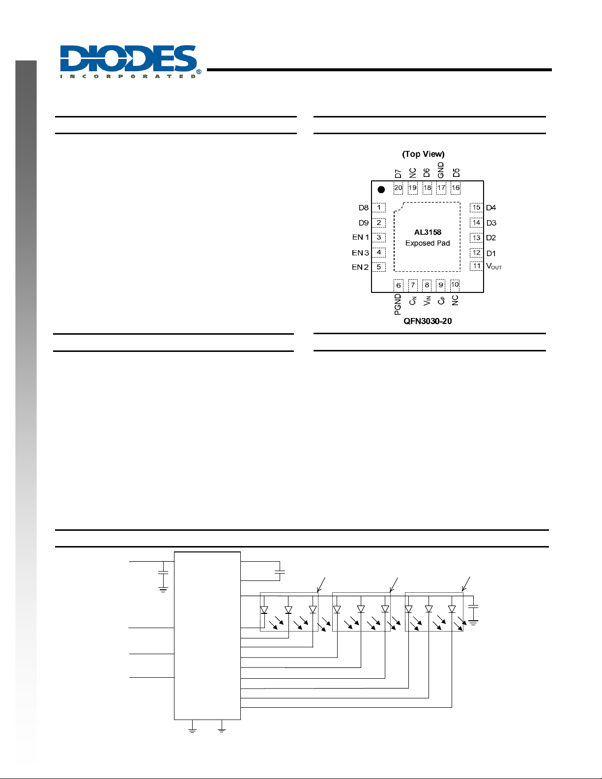
Pin Assignments
The AL3158 is a low noise, constant frequency charge pump
DC/DC converter that uses a Dual mode load switch (1x), and (2x)
conversion for white LED applications. The AL3158 is capable of
driving three groups of three LED channels at 20mA from a 2.7V to
5.5V input. The current sinks may be operated using three simple
PWM dimming inputs individually or in parallel for driving highercurrent LEDs. Low external part counts (one 1µF flying capacitor
and two 2.2µF capacitors at V
suited for small, battery-powered applications.
and V
IN
) make this part ideally
OUT
AL3158 PWM dimming inputs are used to enable, disable device
and dimming LED current with a fixed default current settings at
20mA or other factory programming options available.
Each output of the AL3158 is equipped with built-in protection for
V
short circuit and auto-disable for LED short conditions. Built-in
OUT
soft-start circuitry prevents excessive inrush current during start-up
and mode switching. A low-current shutdown feature disconnects
the load from V
to reduce quiescent current less than 1µA.
IN
The AL3158 is available in a lead-free, space-saving, thermally
enhanced 20-pin 3 x 3mm QFN package.
Features
NEW PRODUCT
• VIN Range: 2.7V to 5.5V
• Up to 93% Max Power Efficiency
• 1% Current Matching Accuracy Between Channels
• Three simple PWM dimming for RGB or WLED
• Low transition threshold voltage typical 150 mV
• Dual-Mode 1x and 2x Charge Pump
• Drives up to 3 + 3 + 3 Channels of LEDs
Applications
• Mobile Phone White LED Backlighting and Indicators
• PDA White LED Backlighting
• Battery-operated Phone Main and Sub Screen White LED
Backlighting
• 1.2 MHz Constant Switching Frequency
short circuit and Thermal Protections
• V
OUT
• Soft Start for reducing inrush current
• Under Voltage Lockout Protection
• I
<1µA in Shutdown
Q
• Thermally-Enhanced QFN3030-20 Package: Available in “Green”
Molding Compound (No Br, Sb)
• Lead Free Finish/ RoHS Compliant (Note 1)
Notes: 1. EU Directive 2002/95/EC (RoHS). All applicable RoHS exemptions applied. Please visit our website at
http://www.diodes.com/products/lead_free.html
Typical Application Circuit
2.2uF
C
IN
8
V
IN
AL3158
3
EN1
5
EN2
4
EN3
PGND
6
V
IN
EN1
EN2
EN3
AL3158
Document number: DS35047 Rev. 2 - 2
GND
9
C
P
7
C
N
11
V
OUT
D1
LED
12
D1
13
D2
14
D3
15
D4
16
D5
18
D6
20
D7
1
D8
2
D9
17
D2
LED
1uF
C
1
EN1 EN2
D4
D3
LED
LED
D5
LEDD6LEDD7LEDD8LEDD9LED
EN3
2.2uF
C
OUT
1 of 10
www.diodes.com
January 2011
© Diodes Incorporated

Pin Descriptions
Pin Name Pin Number Description
D8 1 Current sink input #8. Connected to VOUT when un-used.
D9 2 Current sink input #9. Connected to VOUT when un-used.
EN1 3 Enable Pin 1
EN3 4 Enable Pin 3
EN2 5 Enable Pin 2
PGND 6 Charge Pump Switch Ground
CN 7 Negative Terminal of Flying Capacitor
VIN 8 Input Power Supply. Requires 2.2µF capacitor between this pin and ground.
CP 9 Positive Terminal of Flying Capacitor
NC 10,19 No-Connect
V
OUT
D1 12 Current sink input #1. Connected to V
D2 13 Current sink input #2. Connected to V
D3 14 Current sink input #3. Connected to V
D4 15 Current sink input #4. Connected to V
NEW PRODUCT
D5 16 Current sink input #5. Connected to V
D6 18 Current sink input #6. Connected to V
GND 17 Ground
D7 20 Current sink input #7. Connected to V
GND EP PAD Exposed Pad (bottom). Connected to GND directly underneath the package.
11
Charge pump output to drive load circuit. Requires 2.2µF capacitor between this pin
and ground.
AL3158
HIGH EFFICIENCY 1x/2x CHARGE PUMP
FOR WHITE LED APPLICATIONS
when un-used.
OUT
when un-used.
OUT
when un-used.
OUT
when un-used.
OUT
when un-used.
OUT
when un-used.
OUT
when un-used.
OUT
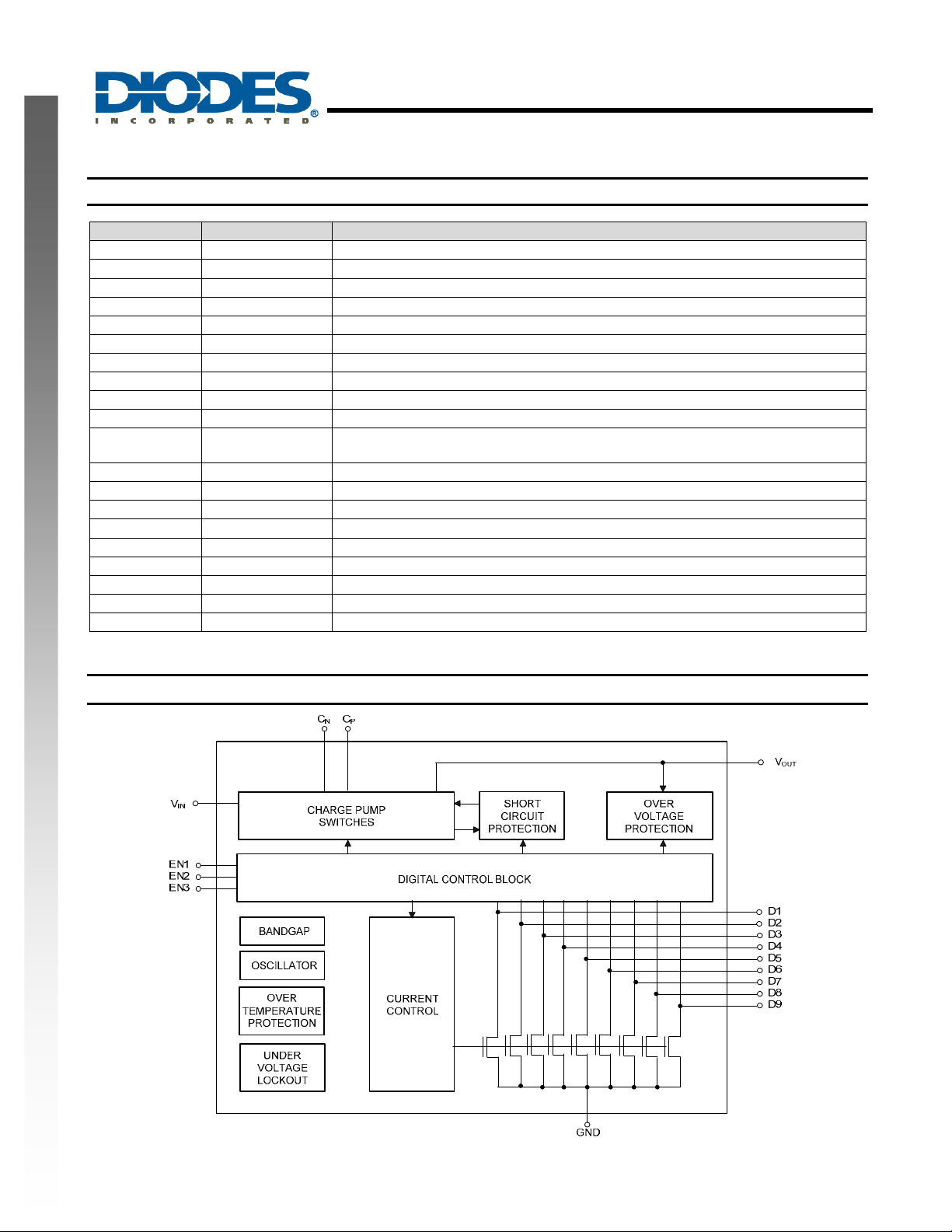
Functional Block Diagram
AL3158
Document number: DS35047 Rev. 2 - 2
2 of 10
www.diodes.com
January 2011
© Diodes Incorporated

HIGH EFFICIENCY 1x/2x CHARGE PUMP
FOR WHITE LED APPLICATIONS
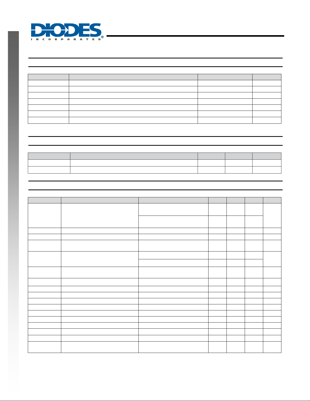
Absolute Maximum Ratings (Note 2)
Symbol Description Rating Unit
ESD HBM Human Body Model ESD Protection 2 KV
ESD MM Machine Model ESD Protection 200 V
VIN Input Voltage -0.3 to 6 V
V
EN1, EN2, EN3 to GND Voltage -0.3 to VIN +0.3 V
EN1,2,3
I
Maximum DC Output Current 270 mA
OUT
TJ Operating Junction Temperature Range 150
T
Maximum Soldering Temperature (at leads, 10 sec) 300
LEAD
Notes: 2. Exceeding Absolute Maximum Ratings will cause permanent damage to the device.
Recommended Operating Conditions
Symbol Parameter Min Max Unit
VIN Input Voltage 2.7 5.5 V
TA Operating Amb ient Temperature -40 85 °C
NEW PRODUCT
Electrical Characteristics (T
Symbol Parameter Test Conditions Min Typ. Max Unit
IQ Quiescent Current
I
Shutdown Current EN1, EN2, EN3 = 0 1 µA
SHDN
I
IDX
I
D-Match
R
Open Loop V
out
VTH
VHS Mode Transition Hysteresis 250 mV
TSS Soft-Start Time 100 µs
Fsw Switching Frequency 1.2 MHz
V
EN1, 2,3 (L)
V
EN1,2,3(H)
T
EN1,2,3 Threshold Low VIN = 2.7V 0.4 V
EN1,2,3 Threshold High VIN = 5.5V 1.4 V
EN1,2,3 Off Timeout 20 ms
EN1,2,3
UVLO VIN Under-Voltage Lockout 1.8 2 2.2 V
I
EN1,2,3 Input Leakag e -1 1 µA
EN1,2,3
T
SHDN
T
HYS
θ
JA
Notes: 3. Determined by the average current levels of all active channels.
4. Determined by the maximum sink current (MAX), the minimum sink current (MIN), and the average sink current (AVG). Two matching numbers are
calculated as (MAX-AVG)/AVG and (AVG-MIN)/AVG. The largest number of the two (worst case) is considered as the matching data.
5. Device mounted on FR-4 substrate, 2"*2", 2oz copper, double-sided PC board, with minimum recommended pad on top layer and
4 vias to bottom layer.
Current Accuracy (Note 3)
SINK
Current Matching Between Any Two
Current Sink Inputs (Note 4)
OUT
1x to 2x Transition Threshold at Any
Pin
I
SINK
Thermal shutdown Protection 160
Thermal shutdown hysteresis 10
Thermal Resistance Junction-to-
Ambient
= 25°C, Vin = 3.6V, CIN = C
A
Resistance
= 2.2µF, C1 = 1µF Unless otherwise noted)
OUT
1x Mode, 3.0≤VIN≤5.5, Active,
No Load Current
2x Mode, 3.0≤VIN≤5.5, Active,
No Load Current
0.3 0.6
2 5
19 20 21 mA
VF: D1:D9 = 3.6V 1 2 %
1x mode 0.5
2 x mode 4.5
= 20mA 150 mV
I
DX
QFN3030-20 (Note 5)
52
AL3158
°C
°C
mA
Ω
°C
°C
o
C/W
AL3158
Document number: DS35047 Rev. 2 - 2
3 of 10
www.diodes.com
January 2011
© Diodes Incorporated
 Loading...