Diodes AH9248 User Manual

High Sensitivity Micropower Omnipolar Hall-Effect Switch AH9248
Data Sheet
General Description
The AH9248 is an ultra-sensitive Hall-effect switch
with digital latched output, mainly designed for
battery-operation, hand-held equi pments.
Special CMOS process is used for low-voltage and
low-power requirement. A chopper stabilized
amplifier improves stability of magnetic switch
points. A sleep-awake logic controls the IC in sleep
time or awake time. This function will reduce the
average operating current of the IC. During the
awake time, the output is changed with the magnetic
flux density. During the sleep time, the output is
latched in its previous state and the current
consumption will reduce to some μA.
The IC switching behaviour is omnipolar, either north
or south pole sufficient strength will turn the output
on. If the magnetic flux density is larger than
operating point (B
it is less than releasing point (B
turned off.
The AH9248 is available in TO-92S-3, SOT-23-3 and
DFN-2×2-3 packages which are optimized for most
applications.
Jul. 2011 Rev. 1. 6 BCD Semiconductor Manufacturing Limited
), the output will be turned on; if
OP
), the output will be
RP
TO-92S-3 SOT-23-3 DFN-2×2-3
Figure 1. Package Types of AH9248
Features
Micropower Operation
•
• 2.5 to 5.5V Power Supply
• Switching for Both Poles of a Magnet
(Omnipolar)
• Stabilized Chopper
• Superior Temperature Stability
• Digital Output Signal
• Built-in Pull-up Resistor (AH9249)
Applications
• Cover Switch in Notebook PC/PDA
• Handheld Wireless Application Awake Switch
• Magnet Switch in Low Duty Cycle Applications
1

Data Sheet
High Sensitivity Micropower Omnipolar Hall-Effect Switch AH9248
Pin Configuration
Z3 Package N Package
(TO-92S-3) (SOT-23-3)
3
2
1
(Front View) (Top View)
OUTPUT
GND
VCC
GND
3
DN Package
Pin 1 Dot
by Marking
VCC
OUTPUT
Figure 2. Pin Configuration of AH9248
(DFN-2×2-3)
1
2
(Top View)
GND
3
21
OUTPUT
VCC
Pin Description
Pin Number
TO-92S-3 SOT-23-3
DFN-2×2-3
1 1 1 VCC Power supply pin
2 3 3 GND Ground pin
3 2 2 OUTPUT Output pin
Jul. 2011 Rev. 1. 6 BCD Semiconductor Manufacturing Limited
2
Pin Name Function

Data Sheet
High Sensitivity Micropower Omnipolar Hall-Effect Switch AH9248
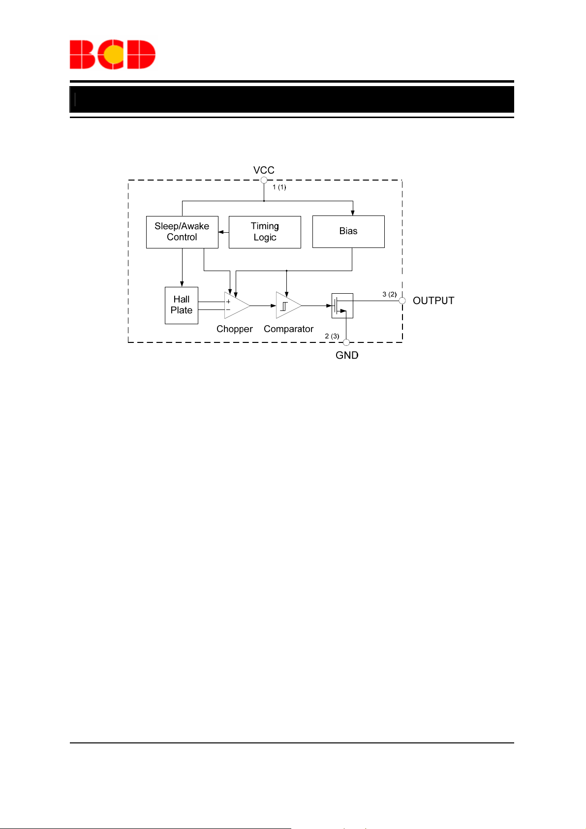
Functional Block Diagram
A (B)
A for TO-92S-3
B for SOT-23-3 and DFN-2×2-3
Figure 3. Functional Block Diagram of AH9248
Jul. 2011 Rev. 1. 6 BCD Semiconductor Manufacturing Limited
3

Data Sheet
High Sensitivity Micropower Omnipolar Hall-Effect Switch AH9248
Ordering Information
AH9248 -
Circuit Type
Package
Z3: TO-92S-3
N: SOT-23-3
DN: DFN-2×2-3
Package Temperature Range Part Number Marking ID Packing Type
G1: Green
Blank: Bulk
TR: Tape and Reel or Ammo
TO-92S-3
-40 to 85°C
SOT-23-3 AH9248NTR-G1 GL1 Tape & Reel
DFN-2×2-3
BCD Semiconductor's Pb-free products, as designated with "G1" suffix in the part number, are RoHS compliant
and green.
AH9248Z3-G1 9248 Bulk
AH9248Z3TR-G1 9248 Ammo
AH9248DNTR-G1 JA Tape & Reel
Jul. 2011 Rev. 1. 6 BCD Semiconductor Manufacturing Limited
4

Data Sheet
High Sensitivity Micropower Omnipolar Hall-Effect Switch AH9248
Absolute Maximum Ratings (TA=25°C, Note 1)
Parameter Symbol Value Unit
Supply Voltage VCC 7 V
Supply Current (Fault) ICC 6 mA
Output Voltage V
Output Current I
Magnetic Flux Density B Unlimited Gauss
Power Dissipation PD
Storage T empera ture T
Junction Temperature TJ 150
ESD (Machine Model) (Note 2) ESD 200 V
7 V
OUT
2 mA
OUT
TO-92S-3 400
SOT-23-3 230
DFN-2×2-3 230
-55 to 150
STG
mW
°C
°C
Note 1: Stresses greater than those listed under “Absolute Maximum Ratings” may cause permanent damage to
the device. These are stress ratings only, and functional operation of the device at these or any other conditions
beyond those indicated under “Recommended Operating Conditions” is not implied. Exposure to “Absolute
Maximum Ratings” for extended periods may affect device reliability.
Note 2: Electronic semiconductor products are sensitive to Electro Static Discharge (ESD). Always observe
Electro Static Discharge control procedures whenever handling semiconductor products.
Recommended Operating Conditions
Parameter Symbol Min Max Unit
Supply Voltage VCC 2.5 5.5 V
Operating T emperat ure TOP -40 85
°C
Jul. 2011 Rev. 1. 6 BCD Semiconductor Manufacturing Limited
5
 Loading...