

Page 1
UNIPOLAR HALL-EFF E CT SWITCH
Data Sheet
AH922
General Description
The AH922 is a unipolar Hall-effect one-chip switch
with digital output, solution for sense magnetic field.
It is designed in mixed signal CMOS and chopper
technology. This IC is quite suitable for use in
automotive, industrial and consumer applications.
The two sensors are suited for operation over
extended temperature ranges.
The AH922 Hall-effect switch is combined with a
voltage regulator, Hall-voltage generator, chopper
small-signal amplifier, Schmitt trigger and
open-drain output.
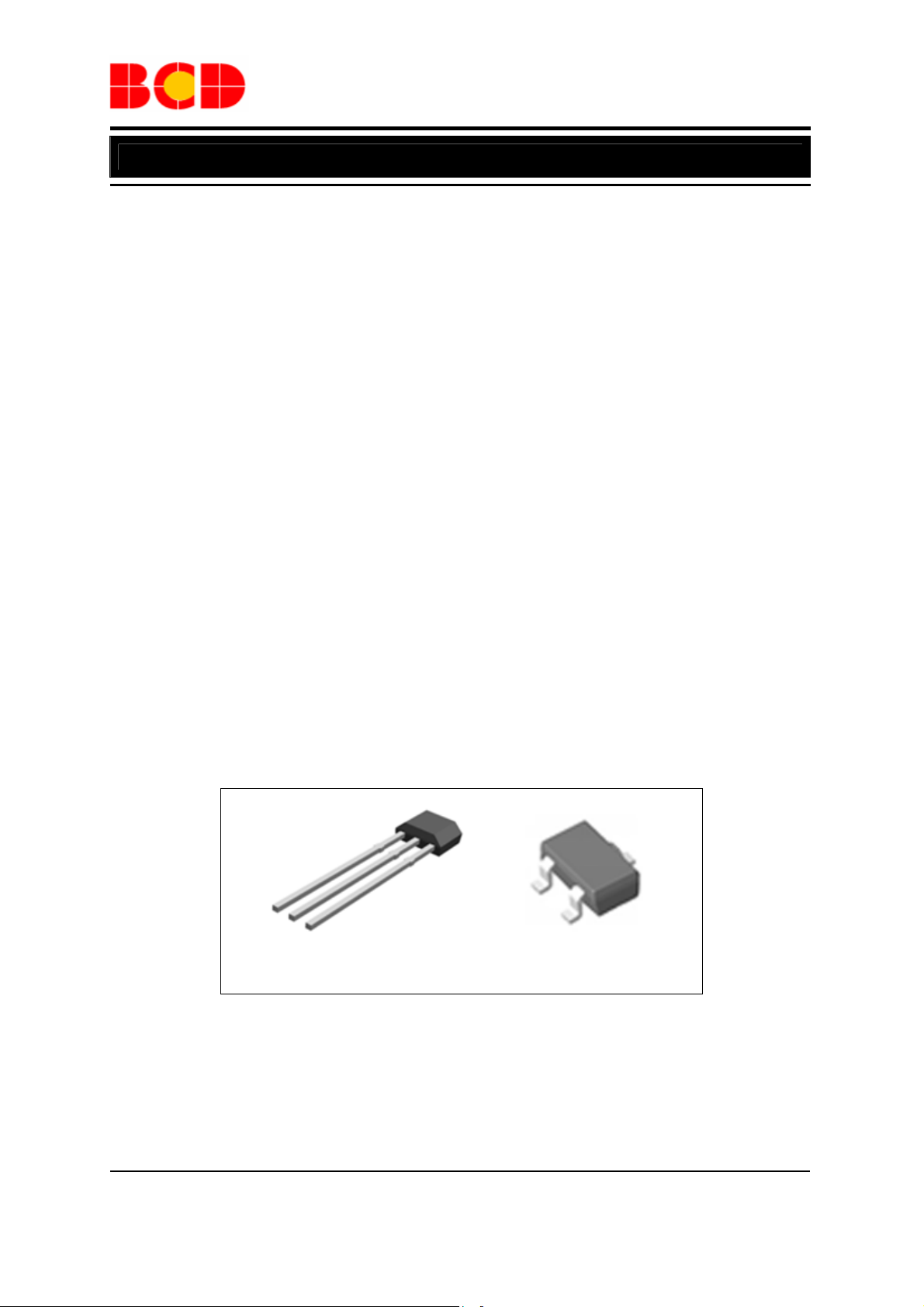
The AH922 is available in TO-92S-3 and SOT-23-3
packages.
Features
• Wide Operating Voltage Range
• Chopper Stabilization
• Extremely Low Switch Point Drift
• Superior T emperature Stability
• High Sensitivity Integrated Hall Sensor
• Solid State Reliability
• Robust EMC Capability
Applications
• 5V/12V DC Brushless Motor/Fan
• Solid State Switch
• Speed Detection
• Revolution Counting
TO-92S-3 SOT-23-3
Figure 1. Package Types of AH922
May 2012 Rev. 1. 1 BCD Semiconductor Manufacturing Limited
1
Page 2
Data Sheet
UNIPOLAR HALL-EFF E CT SWITCH
AH922
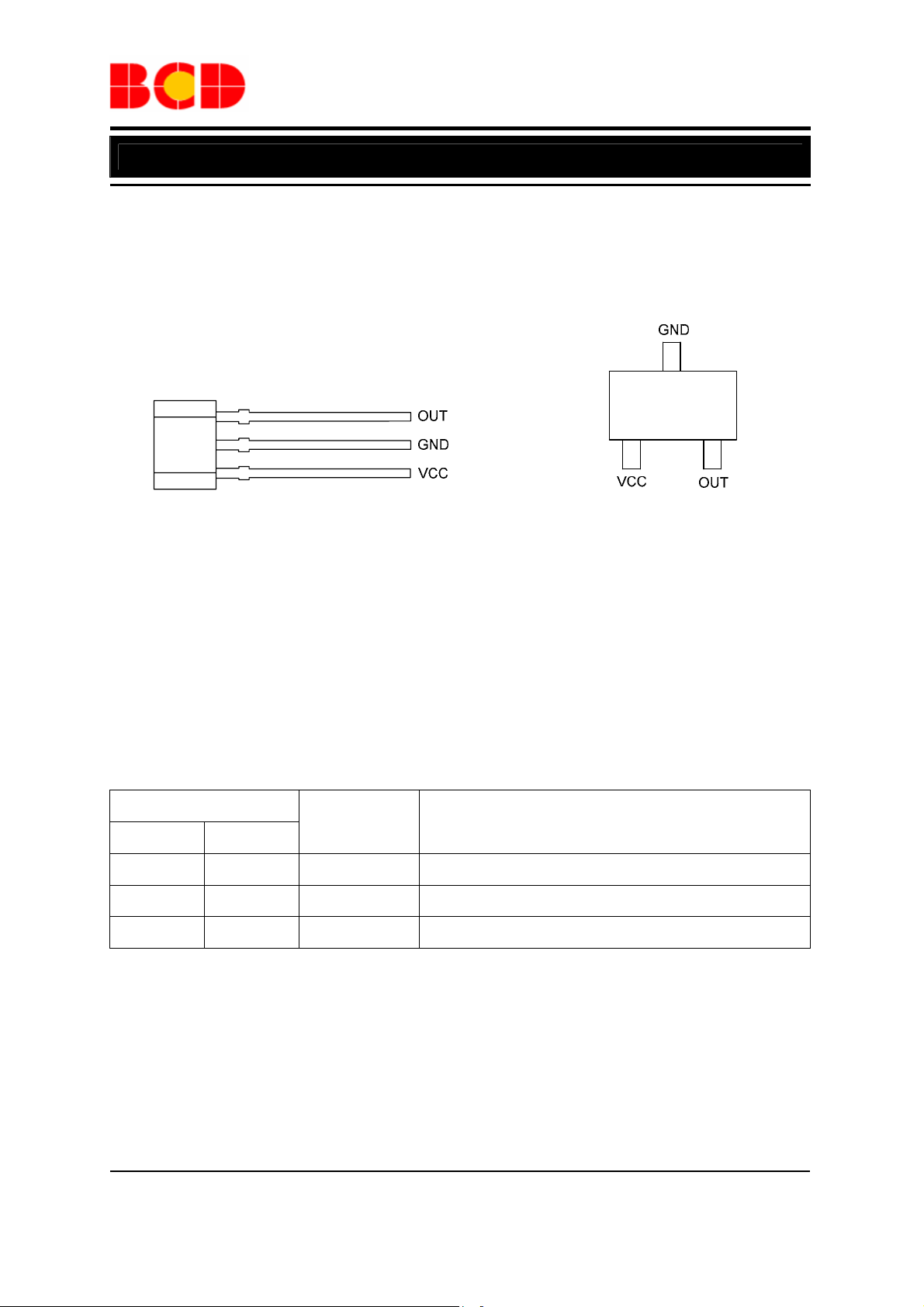
Pin Configuration
Z3 Package N Package
(TO-92S-3) (SOT-23-3)
3
2
1
(Front View) (Top View)
Figure 2. Pin Configuration of AH922
3
21
Pin Description
Pin Number
TO-92S-3 SOT-23-3
1 1 VCC Supply voltage
2 3 GND Ground pin
3 2 OUT Output pin
Pin Name Function
May 2012 Rev. 1. 1 BCD Semiconductor Manufacturing Limited
2
Page 3
Data Sheet
UNIPOLAR HALL-EFF E CT SWITCH
AH922
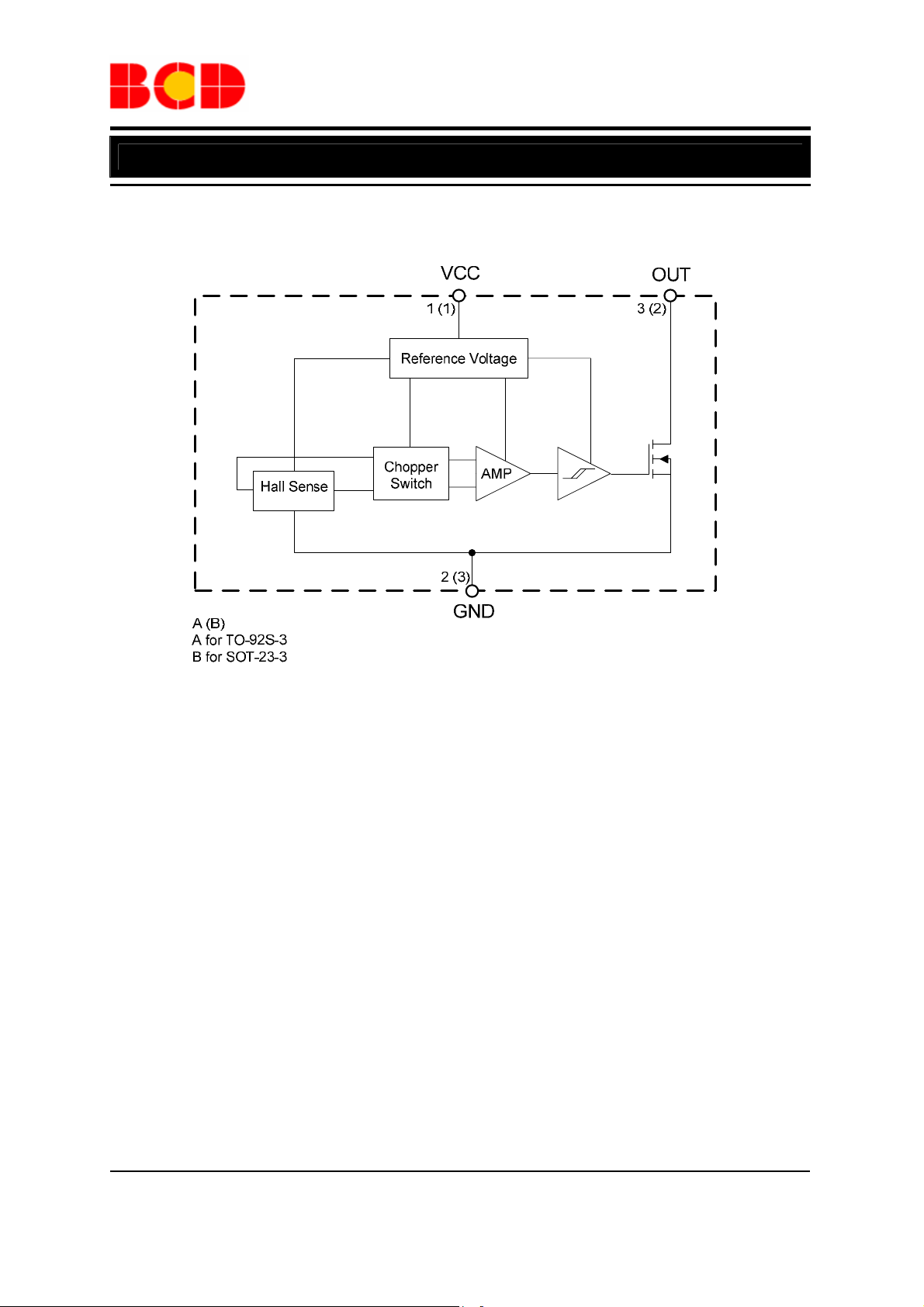
Functional Block Diagram
Figure 3. Functional Block Diagram of AH922
May 2012 Rev. 1. 1 BCD Semiconductor Manufacturing Limited
3
Page 4
Data Sheet
UNIPOLAR HALL-EFF E CT SWITCH
AH922
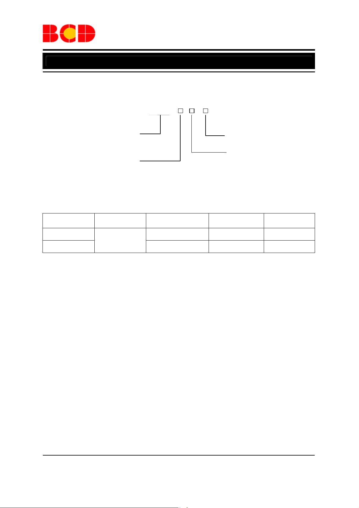
Ordering Information
AH922 -
Circuit Type
Package
Z3: TO-92S-3
N: SOT-23-3
Package
TO-92S-3 AH922Z3-G1 922 Bulk
SOT-23-3
Temperature
Range
-40 to 125°C
Part Number Marking ID Packing Type
AH922NTR-G1 GT4 Tape & Reel
G1: Green
TR: Tape & Reel
Blank: Bulk
BCD Semiconductor's Pb-free products, as designated with "G1" suffix in the part number, are RoHS
compliant and green.
May 2012 Rev. 1. 1 BCD Semiconductor Manufacturing Limited
4
Page 5
Data Sheet
UNIPOLAR HALL-EFF E CT SWITCH
AH922
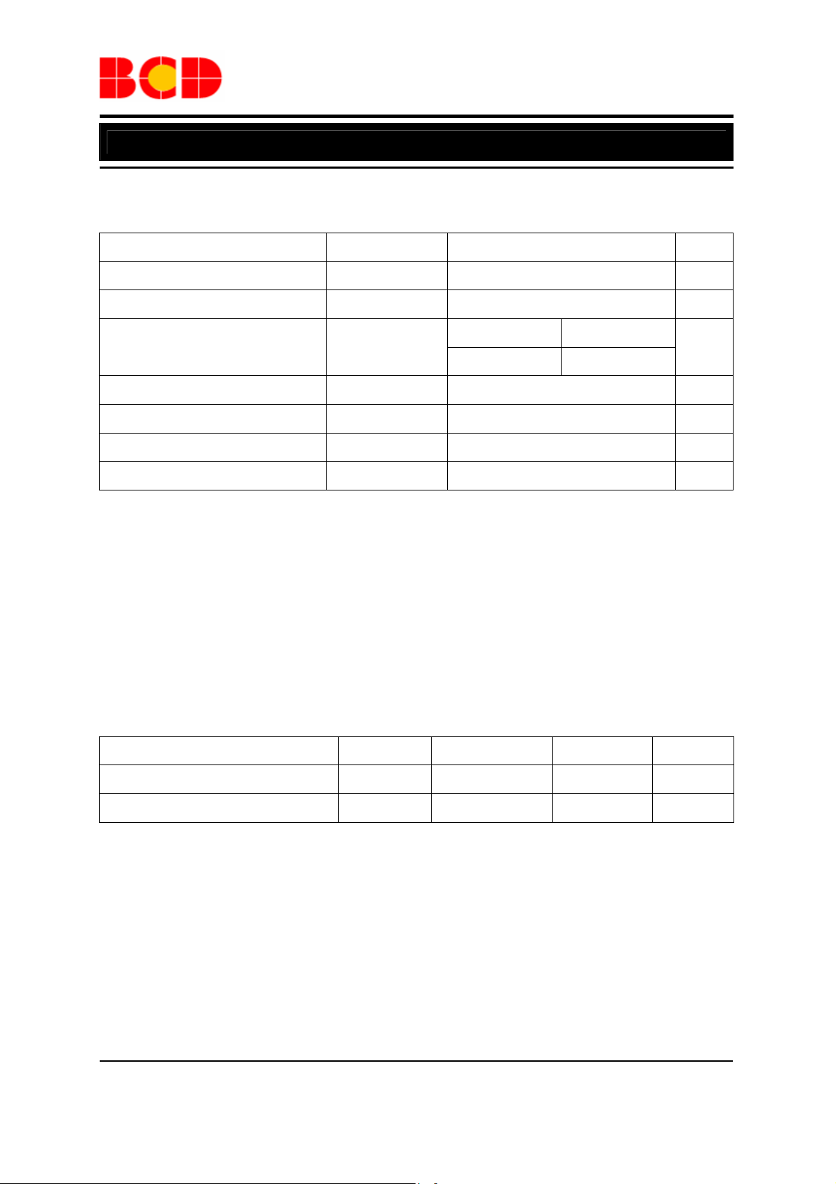
Absolute Maximum Ratings (Note 1)
Parameter Symbol Value Unit
Supply Voltage VCC 24 V
Output Current (Continuous) I
Power Dissipation
Operation T em perature TA -50 to 150 ºC
Storage Temperature T
Maximum Junction Temperature TJ (Max) 165 ºC
ESD (Human Body Model) ESD 4000 V
25 mA
OUT
P
D
-65 to 150 ºC
STG
TO-92S-3 400
SOT-23-3 230
mW
Note 1: Stresses greater than those listed under “Absolute Maximum Ratings” may cause permanent damage to
the device. These are stress ratings only, and functional operation of the device at these or any other conditions
beyond those indicated under “Recommended Operating Conditions” is not implied. Exposure to “Absolute
Maximum Ratings” for extended periods may affect device reliability.
Recommended Operating Conditions
Parameter Symbol Min Max Unit
Supply Voltage V
Operating Ambient Temperature TA -40 125 ºC
CC
3.5 22 V
May 2012 Rev. 1. 1 BCD Semiconductor Manufacturing Limited
5
Page 6

Data Sheet
UNIPOLAR HALL-EFF E CT SWITCH
AH922
Electrical Characteristics
V
=12V, TA=25°C, unless otherwise specified.
CC
Parameter Symbol Conditions Min Typ Max Unit
Supply Voltage VCC Operating 3.5 12 22 V
VCC=12V, B<BRP 3 5 mA
Supply Current ICC
V
=12V, B>BOP 3 5 mA
CC
Saturation Voltage V
Output Leakage Current I
Output Rising Time t
Output Falling Time t
I
SAT
LEAKAGE
RISING
FALLING
OUT
V
OUT
=1kΩ,CL=20pF
R
L
=1kΩ,CL=20pF
R
L
=20mA, B>B
=20V, B<BRP 0.1 5
OP
185 500 mV
0.4 2
0.4 2
µA
µs
µs
Magnetic Characteristics
V
=12V, TA=25°C, unless otherwise specified.
CC
Parameter Symbol Min Typ Max Unit
Operating point BOP 80 110 140 Gauss
Releasing point BRP 35 65 95 Gauss
Hysteresis B
20 45 70 Gauss
HYS
May 2012 Rev. 1. 1 BCD Semiconductor Manufacturing Limited
6
Page 7

Data Sheet
UNIPOLAR HALL-EFF E CT SWITCH
AH922
Magnetic Characteristics (Continued)
Figure 4. Magnetic Flux Density of AH922
May 2012 Rev. 1. 1 BCD Semiconductor Manufacturing Limited
7
Page 8

Data Sheet
UNIPOLAR HALL-EFF E CT SWITCH
AH922
Test Circuit and Test Conditions
Figure 5. Test Circuit of AH922
Figure 6. Test Condition of AH922 (Supply Current)
Note 2: The output is open during measurement.
Note 3: The device is put under the magnetic field: B<B
May 2012 Rev. 1. 1 BCD Semiconductor Manufacturing Limited
RP.
8
Page 9

Data Sheet
UNIPOLAR HALL-EFF E CT SWITCH
AH922
Test Circuit and Test Conditions (Continued)
Figure 7. Test Condition of AH922 (Output Saturation Voltage)
Note 4: The output saturatio n volt a ge V
Note 5: The device is put under the magnetic field: B>B
is measured at VCC=12V.
SAT
OP.
Figure 8. Test Condition of AH922 (Output Leakage Current)
Note 6: The device is put under the magnetic field: B<B
RP.
Note 7: VDC=12V.
May 2012 Rev. 1. 1 BCD Semiconductor Manufacturing Limited
9
Page 10

Data Sheet
UNIPOLAR HALL-EFF E CT SWITCH
AH922
Typical Performance Characteristics
4.0
3.5
3.0
(mA)
CC
I
2.5
2.0
1.5
2 4 6 8 1012141618202224262830
VCC (V)
Figure 9. I
vs. VCC Figure 10. ICC vs. TA
CC
4.5
4.0
3.5
3.0
(mA)
2.5
CC
I
2.0
VCC=3.5V
VCC=5V
1.5
VCC=12V
VCC=24V
1.0
-25 0 25 50 75 100 125
TA (oC)
160
140
120
100
80
(mV)
SAT
V
60
40
20
0
0 5 10 15 20 25
I
(mA)
OUT
220
200
180
160
(mV)
140
SAT
V
120
100
80
VCC=3.5V
VCC=5V
VCC=12V
VCC=24V
I
=20mA
OUT
-25 0 25 50 75 100 125
TA (oC)
Figure 11. V
SAT
vs. I
OUT
Figure 12. V
SAT
vs. T
A
May 2012 Rev. 1. 1 BCD Semiconductor Manufacturing Limited
10
Page 11

Data Sheet
UNIPOLAR HALL-EFF E CT SWITCH
AH922
Typical Performance Characteristics (Continued)
150
140
130
120
110
100
(Gauss)
90
HYS
/B
80
RP
/B
70
OP
B
60
50
40
30
2 4 6 8 10 12 14 16 18 20 22 24 26
VCC (V)
B
OP
B
RP
B
HYS
150
140
130
120
110
100
(Gauss)
90
HYS
80
/B
RP
70
/B
OP
60
B
50
40
30
20
-50 -25 0 25 50 75 100 125 150
Figure 13. BOP/ BRP/ B
HYS
vs. V
CC
Figure 14. BOP/ BRP/ B
450
400
350
300
250
(mW)
D
200
P
150
100
50
0
0 25 50 75 100 125 150
TA (oC)
SOT-23-3
TO-92S-3
Figure 15. PD vs. TA
TA (oC)
HYS
vs. TA
B
OP
B
RP
B
HYS
May 2012 Rev. 1. 1 BCD Semiconductor Manufacturing Limited
11
Page 12

Data Sheet
UNIPOLAR HALL-EFF E CT SWITCH
AH922
T ypical Application
C
Figure 16. Typical Application Circuit of AH922
0.1 F
L
R
Output
L
V
CC
May 2012 Rev. 1. 1 BCD Semiconductor Manufacturing Limited
12
Page 13

Data Sheet
UNIPOLAR HALL-EFF E CT SWITCH
AH922
Mechanical Dimensions
TO-92S-3 Unit: mm(inch)
°
°
May 2012 Rev. 1. 1 BCD Semiconductor Manufacturing Limited
13
Page 14

Data Sheet
UNIPOLAR HALL-EFF E CT SWITCH
AH922
Mechanical Dimensions (Continued)
SOT-23-3 Unit: mm(inch)
2.820(0.111)
3.020(0.119)
1.300(0.051)
1.600(0.063)
0.300(0.012)
Package Sensor
Location
2.650(0.104)
2.950(0.116)
1.500(0.059)
1.700(0.067)
0.200(0.008)
0.600(0.024)
0.100(0.004)
0.200(0.008)
0.950(0.037)
TYP
MAX.
1.450(0.057)
1.800(0.071 )
2.000(0.079)
0.770(0.030)
1.070(0.042)
0.300(0.012
0.500(0.020)
0.900(0.035)
1.300(0.051)
)
0.000(0.000)
0.150(0.006)
0
8
May 2012 Rev. 1. 1 BCD Semiconductor Manufacturing Limited
14
Page 15

BCD Semiconductor Manufacturing Limited
IMPORTANT NOTICE
IMPORTANT NOTICE
BCD Semiconductor Manufacturing Limited reserves the right to make changes without further notice to any products or specifi-
BCD Semiconductor Manufacturing Limited reserves the right to make changes without further notice to any products or specifi-
cations herein. BCD Semiconductor Manufacturing Limited does not assume any responsibility for use of any its products for any
cations herein. BCD Semiconductor Manufacturing Limited does not assume any responsibility for use of any its products for any
particular purpose, nor does BCD Semiconductor Manufacturing Limited assume any liability arising out of the application or use
particular purpose, nor does BCD Semiconductor Manufacturing Limited assume any liability arising out of the application or use
of any its products or circuits. BCD Semiconductor Manufacturing Limited does not convey any license under its patent rights or
of any its products or circuits. BCD Semiconductor Manufacturing Limited does not convey any license under its patent rights or
other rights nor the rights of others.
other rights nor the rights of others.
http://www.bcdsemi.com
MAIN SITE
MAIN SITE
- Headquarters
BCD Semiconductor Manufacturing Limited
BCD Semiconductor Manufactur ing Limited
- Wafer Fab
No. 1600, Zi Xing Road, Shanghai ZiZhu Science-based Industrial Park, 200241, China
Shanghai SIM-BCD Semiconductor Manufacturing Limited
Tel: +86-21-24162266, Fax: +86-21-24162277
800, Yi Shan Road, Shanghai 200233, China
Tel: +86-21-6485 1491, Fax: +86-21-5450 0008
REGIONAL SALES OFFICE
Shenzhen Office
REGIONAL SALES OFFICE
Shanghai SIM-BCD Semiconductor Manufacturing Co., Ltd., Shenzhen Office
Shenzhen Office
Unit A Room 1203, Skyworth Bldg., Gaoxin Ave.1.S., Nanshan District, Shenzhen,
Shanghai SIM-BCD Semiconductor Manufacturing Co., Ltd. Shenzhen Office
China
Advanced Analog Circuits (Shanghai) Corporation Shenzhen Office
Tel: +86-755-8826 7951
Room E, 5F, Noble Center, No.1006, 3rd Fuzhong Road, Futian District, Shenzhen 518026, China
Fax: +86-755-8826 7865
Tel: +86-755-8826 7951
Fax: +86-755-8826 7865
- Wafer Fab
BCD Semiconductor Manufacturing Limited
Shanghai SIM-BCD Semiconductor Manufacturing Co., Ltd.
- IC Design Group
800 Yi Shan Road, Shanghai 200233, China
Advanced Analog Circuits (Shanghai) Corporation
Tel: +86-21-6485 1491, Fax: +86-21-5450 0008
8F, Zone B, 900, Yi Shan Road, Shanghai 200233, China
Tel: +86-21-6495 9539, Fax: +86-21-6485 9673
Taiwan Office
BCD Semiconductor (Taiwan) Company Limited
Taiwan Office
4F, 298-1, Rui Guang Road, Nei-Hu District, Taipei,
BCD Semiconductor (Taiwan) Company Limited
Tai wan
4F, 298-1, Rui Guang Road, Nei-Hu District, Taipei,
Tel: +886-2-2656 2808
Taiwan
Fax: +886-2-2656 2806
Tel: +886-2-2656 2808
Fax: +886-2-2656 2806
USA Office
BCD Semiconductor Corp.
USA Office
30920 Huntwood Ave. Hayward,
BCD Semiconductor Corporation
CA 94544, USA
30920 Huntwood Ave. Hayward,
Tel : +1-510-324-2988
CA 94544, U.S.A
Fax: +1-510-324-2788
Tel : +1-510-324-2988
Fax: +1-510-324-2788
 Loading...