Diodes 74LVC1G125 User Manual
74LVC1G125
SINGLE BUFFER GATE WITH 3-STATE OUTPUT
Description
The 74LVC1G125 is a single non-inverting buffer/bus driver with a 3-
state output. The output enters a high impedance state when a HIGH-
level is applied to the output enable (OE) pin. The device is designed
for operation with a power supply range of 1.65V to 5.5V. The inputs
are tolerant to 5.5V allowing this device to be used in a mixed voltage
environment. The device is fully specified for partial power down
applications using I
preventing damaging current backflow when the device is powered
down.
OFF
. The I
circuitry disables the output
OFF
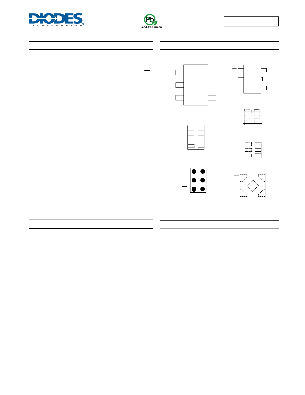
Pin Assignments
( Top View )
OE
1
A
2
GND
SOT25 / SOT353
(
Top View
OE
A
GND
X2-DFN1410-6
(
Bottom View
3
GND
2
A
OE
1
X2-DFN1409-6
Chip Scale
Alternative
1
245
3
)
6
Vcc
NC
Y
( Top View )
OE
A
GND
OE
1
2
3
SOT553
(
Top View
1
OE
Future
2
A
Product
34
GND
X1-DFN1010-6
(
Top View
1
OE
2
A
34
GND
X2-DFN1010-6
(Top View)
1
GND
2
A
Vcc
5
43
Y
)
4
Y
NC
5
Vcc
6
X2-DFN0808-4
Packages not to scale
5
Vcc
4
Y
)
6
Vcc
5
NC
Y
)
6
Vcc
5
NC
Y
Vcc
5
3
Y
4
Features
Wide Supply Voltage Range from 1.65 to 5.5V
± 24mA Output Drive at 3.3V
CMOS low power consumption
I
Inputs accept up to 5.5V
ESD Protection Tested per JESD 22
Latch-Up Exceeds 100mA per JESD 78, Class I
Range of Package Options
Direct Interface with TTL Levels
Supports Partial-Power-Down Mode Operation
OFF
o Exceeds 200-V Machine Model (A115)
o Exceeds 2000-V Human Body Model (A114)
o Exceeds 1000-V Charged Device Model (C101)
Applications
Voltage Level Shifting
Bus Driver / Repeater
Power Down Signal Isolation
General Purpose Logic
Wide array of products such as:
o PCs, networking, notebooks, netbooks, PDAs
o Tablet Computers, E-readers
o Computer peripherals, hard drives, CD/DVD ROM
o TV, DVD, DVR, set top box
o Cell Phones, Personal Navigation / GPS
o MP3 players ,Cameras, Video Recorders
Totally Lead-Free & Fully RoHS Compliant (Notes 1 & 2)
Halogen and Antimony Free. “Green” Device (Note 3)
Notes: 1. No purposely added lead. Fully EU Directive 2002/95/EC (RoHS) & 2011/65/EU (RoHS 2) compliant.
2. See http://www.diodes.com for more information about Diodes Incorporated’s definitions of Halogen- and Antimony-free, "Green" and Lead-free.
3. Halogen- and Antimony-free "Green” products are defined as those which contain <900ppm bromine, <900ppm chlorine (<1500ppm total Br + Cl)
and < 1000ppm antimony compounds.
74LVC1G125
Document number: DS32202 Rev. 7 - 2
1 of 15
www.diodes.com
March 2014
© Diodes Incorporated
Ordering Information
r
X
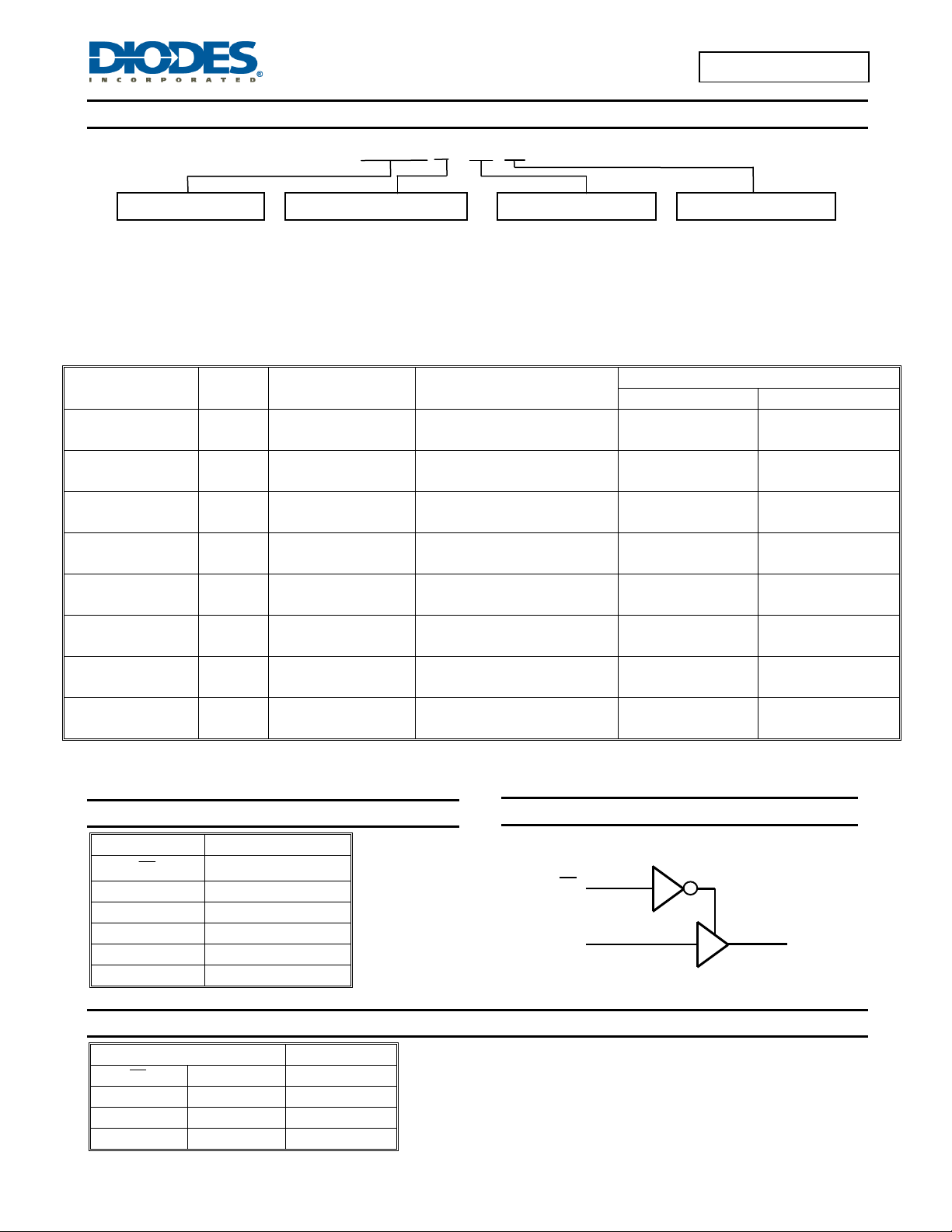
74 LVC1G 125 XXX -7
Logic Device
74 : Logic Prefix 125: 3-State Buffe
LVC : 1.65 to 5.5 V OE active low SE : SOT353
Logic Family Z : SOT553
1G : One Gate FS3 : X2-DFN0808-4
FW5 : X1-DFN1010-6
FW4 :X2-DFN1010-6
F
FZ4 : X2- DFN1410-6
Function Package Packing
W5 : SOT25 -7 : 7” Tape & Reel
4 : X2- DFN1409-6
74LVC1G125
Device
74LVC1G125W5-7 W5 SOT25
74LVC1G125SE-7 SE SOT353
74LVC1G125Z-7 Z SOT553
74LVC1G125FS3-7 FS3 X2-DFN0808-4
74LVC1G125FW5-7
(Future Product)
74LVC1G125FW4-7 FW4 X2-DFN1010-6
74LVC1G125FX4-7 FX4
74LVC1G125FZ4-7 FZ4 X2-DFN1410-6
Notes: 4. Pad layout as shown on Diodes Inc. suggested pad layout document AP02001, which can be found on our website at
http://www.diodes.com/datasheets/ap02001.pdf.
5. The taping orientation is located on our website at http://www.diodes.com/datasheets/ap02007.pdf
Package
Code
FW5
Package
(Notes 4, 5)
1.6mm X 1.6 mm X 0.62mm
0.9mm X 0.9 mm X 0.35mm
0.5mm pad pitch (diamond)
X1-DFN1010-6
(Future Product)
X2-DFN1409-6
(Chip scale alternative)
Package
Size
3.0mm X 2.8mm X 1.2mm
0.95mm lead pitch
2.0mm X 2.0mm X 1.1mm
0.65mm lead pitch
0.5mm lead pitch
1.0mm X 1.0mm X 0.5mm
0.35mm pad pitch
1.0mm X 1.0mm X 0.4mm
0.35mm pad pitch
1.4mm X 0.9mm X 0.4mm
0.5mm pad pitch
1.4mm X 1.0mm X 0.4mm
0.5mm pad pitch
Quantity Part Number Suffix
3000/Tape & Reel -7
3000/Tape & Reel -7
4000/Tape & Reel -7
5000/Tape & Reel -7
5000/Tape & Reel -7
5000/Tape & Reel -7
5000/Tape & Reel -7
5000/Tape & Reel -7
7” Tape and Reel
Pin Descriptions
Pin Name Description
OE
A Data Input
GND Ground
Y Data Output
VCC
NC No Connection
Output Enable
Supply Voltage
Logic Diagram
1
OE
24
A
Y
Function Table
Inputs Output
OE
L H H
L L L
H X Z
74LVC1G125
Document number: DS32202 Rev. 7 - 2
A Y
2 of 15
www.diodes.com
March 2014
© Diodes Incorporated
74LVC1G125
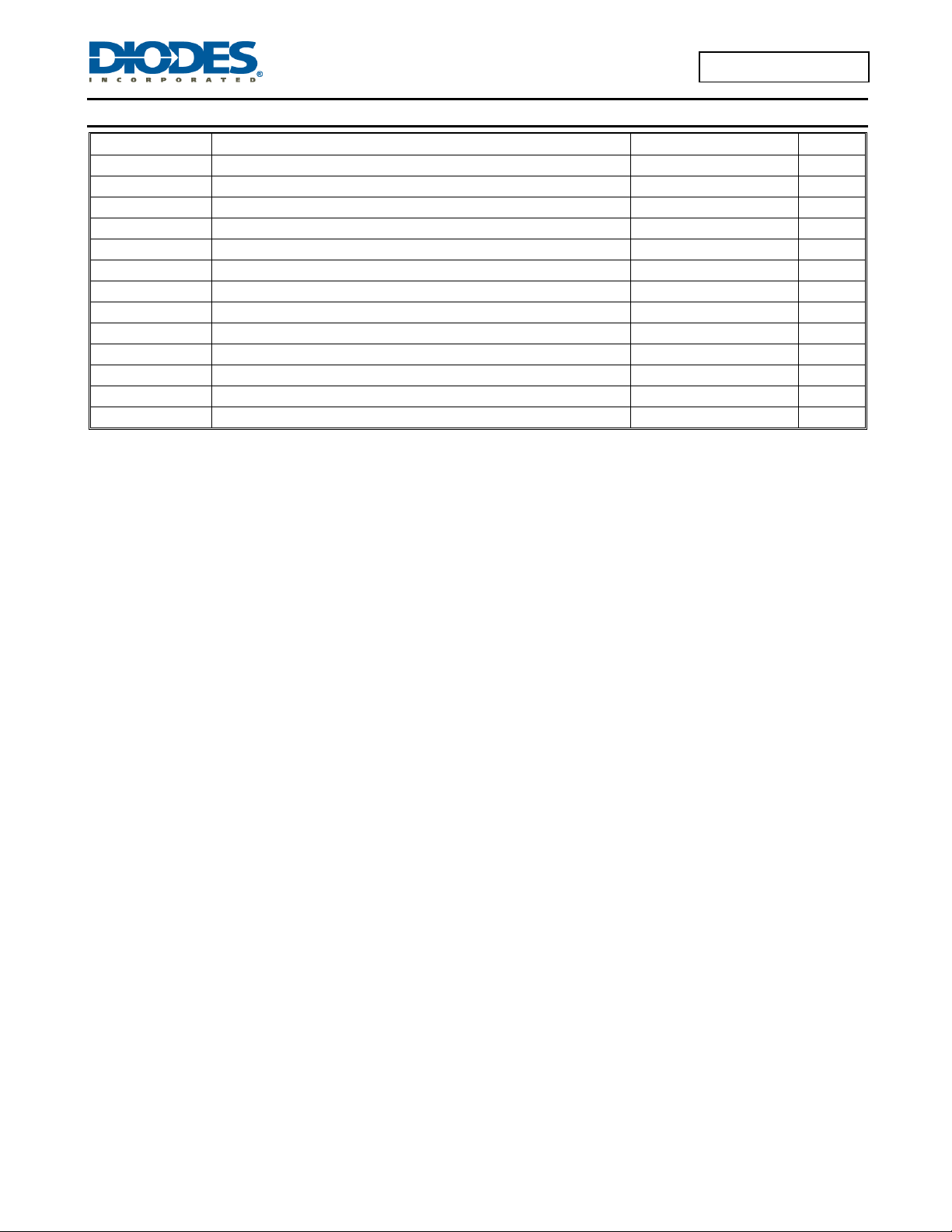
Absolute Maximum Ratings (Notes 6, 7)
Symbol Description Rating Unit
ESD HBM Human Body Model ESD Protection 2 kV
ESD CDM Charged Device Model ESD Protection 1 kV
ESD MM Machine Model ESD Protection 200 V
VCC
VI
VO Voltage applied to output in high impedance or I
VO
IIK Input Clamp Current VI < 0
IOK
IO
I
CC, IGND
TJ
T
STG
Notes: 6. Stresses beyond the absolute maximum may result in immediate failure or reduced reliability. These are stress values and device
7. Forcing the maximum allowed voltage could cause a condition exceeding the maximum current or conversely forcing the maximum current could
operation should be within recommend values.
Supply Voltage Range -0.5 to 6.5 V
Input Voltage Range -0.5 to 6.5 V
state
OFF
Voltage applied to output in high or low state
Output Clamp Current -50 mA
Continuous Output Current ±50 mA
Continuous Current Through V
Operating Junction Temperature -40 to +150 °C
Storage Temperature -65 to +150 °C
or GND
CC
-0.5 to 6.5 V
-0.5 to VCC +0.5
-50 mA
±100 mA
V
74LVC1G125
Document number: DS32202 Rev. 7 - 2
3 of 15
www.diodes.com
March 2014
© Diodes Incorporated
74LVC1G125
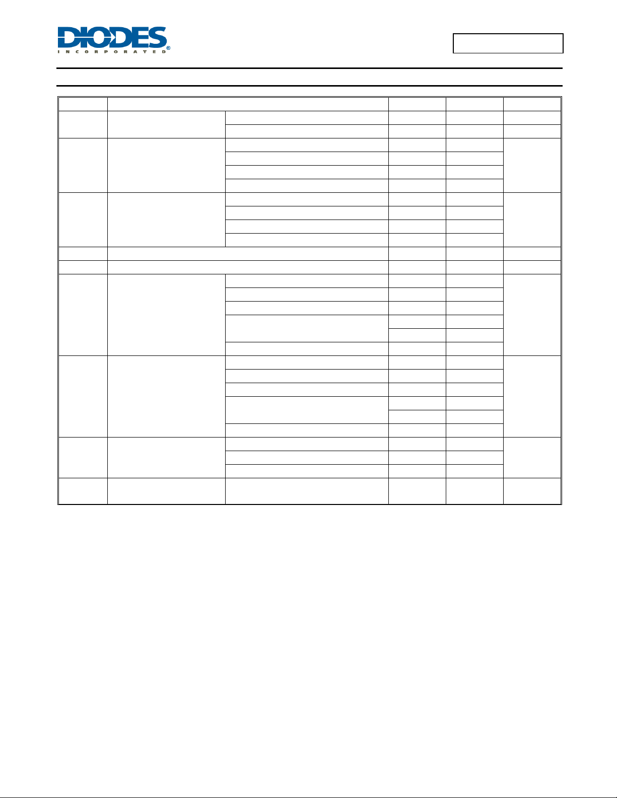
Recommended Operating Conditions (Note 8)
Symbol Parameter Min Max Unit
VCC
V
VIL
VO
IOH
IOL
∆t/∆V
TA
Note: 8. Unused inputs should be held at VCC or Ground.
Operating Voltage
High-Level Input Voltage
IH
Low-level Input voltage
VI
Input Voltage 0 5.5 V
Output Voltage 0
High-Level Output Current
Low-Level Output Current
Input Transition Rise or Fall
Rate
Operating Free-Air
Temperature
Operating 1.65 5.5 V
Data retention only 1.5 — V
= 1.65V to 1.95V 0.65 X VCC
V
CC
VCC = 2.3V to 2.7V
VCC = 3V to 3.6V
VCC = 4.5V to 5.5V 0.7 X VCC
= 1.65V to 1.95V
V
CC
VCC = 2.3V to 2.7V
VCC = 3V to 3.6V
VCC = 4.5V to 5.5V
= 1.65V
V
CC
VCC = 2.3V
VCC = 2.7V
VCC = 3V
VCC = 4.5V
= 1.65V
V
CC
VCC = 2.3V
VCC = 2.7V
VCC = 3V
VCC = 4.5V
V
= 1.8V ± 0.15V, 2.5V ± 0.2V
CC
VCC = 3.3V ± 0.3V
VCC = 5V ± 0.5V
— -40 +125 °C
1.7 —
2 —
—
— 0.7
— 0.8
—
— -4
— -8
— -12
— -16
— -24
— -32
— 4
— 8
— 12
— 16
— 24
— 32
— 20
— 10
— 5
—
—
0.35 X VCC
0.3 X VCC
VCC
V
V
V
mA
mA
ns/V
74LVC1G125
Document number: DS32202 Rev. 7 - 2
4 of 15
www.diodes.com
March 2014
© Diodes Incorporated
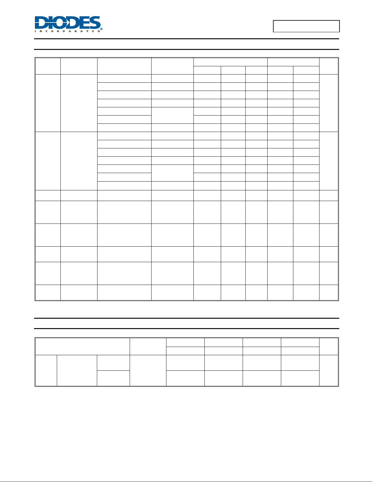
74LVC1G125
Electrical Characteristics (All typical values are at V
Symbol Parameter Test Conditions
I
= -100μA
OH
IOH = -4mA
IOH = -8mA
IOH = -12mA
IOH = -16mA
VOH
High-Level
Output Voltage
IOH = -24mA
IOH = -32mA
I
= 100μA
OL
IOL = 4mA
IOL = 8mA
VOL
Low-Level
Output Voltage
IOL = 12mA
IOL = 16mA
IOL = 24mA
I
= 32mA
OL
II
Input Current
VI = 5.5 V or GND
Power Down
I
OFF
Leakage
VI or VO = 5.5V
Current
Z State
IOZ
Leakage
VO =0 to 5.5V
Current
= 5.5V or GND
V
ICC
∆ICC
Ci
Supply Current
Additional
Supply Current
Input
Capacitance
I
I
=0
O
One input at V
CC
Other inputs at V
GND
Vi = V
– or GND
CC
–0.6V
or
CC
V
CC
1.65V to 5.5V
1.65V 1.2 — — 0.95 —
2.3V 1.9 — — 1.7 —
2.7V 2.2 — — 1.9 —
3V
4.5V 3.8 — — 3.4 —
1.65V to 5.5V — — 0.1 — 0.1
1.65V — — 0.45 — 0.7
2.3V — — 0.3 — 0.45
2.7V — — 0.4 — 0.6
3V
4.5V
0 to 5.5V — ± 0.1 ±5 — ± 100 μA
0V — — ±10 — ±200 μA
3.6V — 0.1 10 — 20 μA
5.5V — 0.1 10 — 200 μA
3V to 5.5V — — 500 — 5000 μA
3.3V — 5 — — — pF
= 3.3V, TA = +25°C)
CC
Min Typ. Max Min Max
V
– 0.1
CC
2.4 — — 2.2 —
2.3 — — 2.0 —
— — 0.4 — 0.6
— —
— —
-40°C to +85°C -40°C to +125°C
V
— —
0.55
0.55
CC
– 0.1
—
—
—
0.8
.8
Unit
V
V
Operating Characteristics
T
= +25°C
A
Parameter
Outputs
Enabled
Outputs
Disabled
Cpd
Power
Dissipation
Capacitance
74LVC1G125
Document number: DS32202 Rev. 7 - 2
Test
Conditions
f = 10MHz
V
= 1.8V VCC = 2.5V VCC = 3.3V VCC = 5V
CC
Typ. Typ. Typ. Typ.
19 19 19 21
2 2 3 4
5 of 15
www.diodes.com
© Diodes Incorporated
Unit
pF
March 2014
 Loading...