Diodes 74LVC1G10 User Manual

SINGLE 3 INPUT POSITIVE NAND GATE
Description
The 74LVC1G10 is a single 3-input positive NAND gate with
a standard push-pull output. The device is designed for
operation with a power supply range of 1.65V to 5.5V. The
inputs are tolerant to 5.5V allowing this device to be used in
a mixed voltage environment. The device is fully specified
for partial power down applications using IOFF. The IOFF
circuitry disables the output preventing damaging current
backflow when the device is powered down.
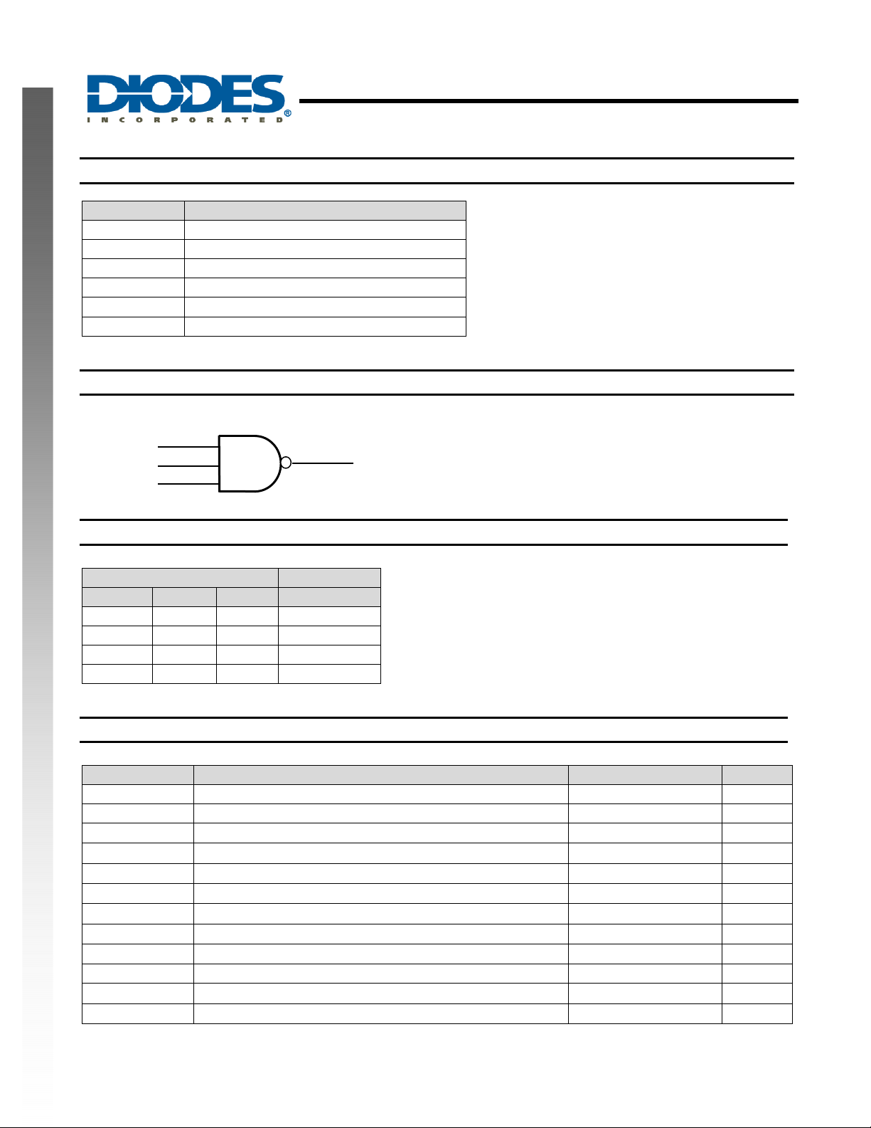
The gate performs the positive Boolean function:
CBAY ••= or CBAY ++=
NEW PRODUCT
Features
• Wide Supply Voltage Range from 1.65V to 5.5V
• ± 24mA Output Drive at 3.3V
• CMOS low power consumption
• IOFF Supports Partial-Power-Down Mode Operation
• Inputs accept up to 5.5V
• ESD Protection Exceeds JESD 22
200-V Machine Model (A115-A)
2000-V Human Body Model (A114-A)
• Latch-Up Exceeds 100mA per JESD 78, Class II
• Range of Package Options
• SOT26, SOT363, DFN1410, and DFN1010: Available in
“Green” Molding Compound (no Br, Sb)
• Lead Free Finish/ RoHS Compliant (Note 1)
Notes: 1. EU Directive 2002/95/EC (RoHS). All applicable RoHS exemptions applied. Please visit our website at
http://www.diodes.com/products/lead_free.html.
A
GND
B
GND
Applications
• Voltage Level Shifting
• General Purpose Logic
• Power Down Signal Isolation
• Wide array of products such as:
o PCs, networking, notebooks, netbooks, PDAs
o Computer peripherals, hard drives, CD/DVD ROM
o TV, DVD, DVR, set top box
o Cell Phones, Personal Navigation / GPS
o MP3 players ,Cameras, Video Recorders
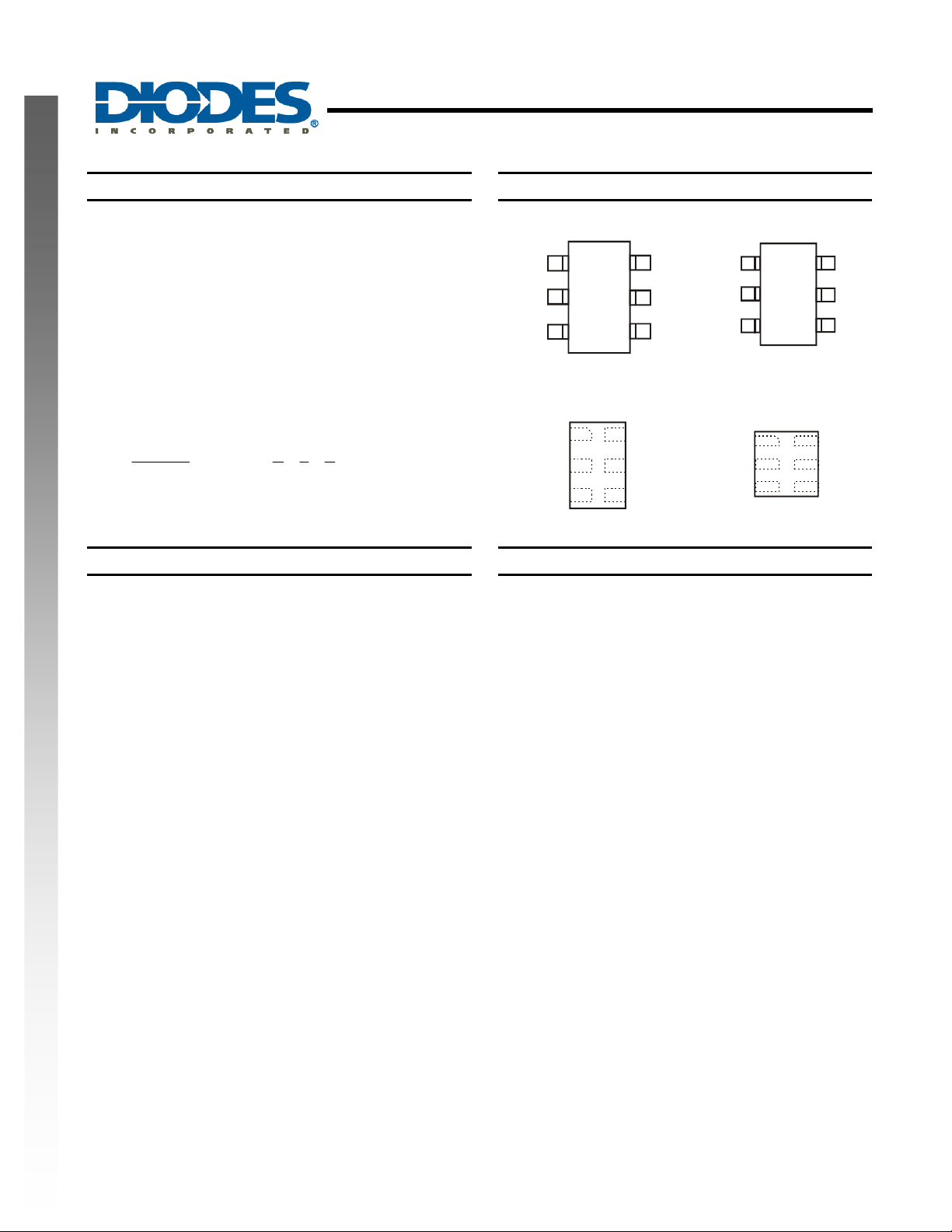
Pin Assignments
(Top View)
1
2
3
SOT26
(Top View)
A
1
6
2
5
3
B
4
DFN1410
74LVC1G10
(Top View)
GND
1
A
2
3
B
6
C
5
V
CC
4
Y
SOT363
GND
(Top View)
1
A
2
3
B
DFN1010
C
V
CC
Y
6
C
5
V
CC
4
Y
6
C
5
V
CC
4
Y
74LVC1G10
Document number: DS35121 Rev. 3 - 2
1 of 13
www.diodes.com
October 2011
© Diodes Incorporated

Pin Descriptions
Pin Name Description
GND Ground
VCC
Logic Diagram
NEW PRODUCT
Function Table
A Data Input
B Data Input
Y Data Output
Supply Voltage
C Data Input
1
A
3
B
6
C
74LVC1G10
SINGLE 3 INPUT POSITIVE NAND GATE
4
Y
Inputs Output
A B C Y
H H H L
L X X H
X L X H
X X L H
Absolute Maximum Ratings (Note 2)
Symbol Description Rating Unit
ESD HBM Human Body Model ESD Protection 2 KV
ESD MM Machine Model ESD Protection 200 V
VCC
VI
VO Voltage applied to output in high impedance or I
VO
IIK Input Clamp Current VI<0
IOK
IO
Continuous current through Vdd or GND ±100 mA
TJ
T
STG
Notes: 2. Stresses beyond the absolute maximum may result in immediate failure or reduced reliability. These are stress values and device
operation should be within recommend values.
Supply Voltage Range -0.5 to 6.5 V
Input Voltage Range -0.5 to 6.5 V
state
OFF
Voltage applied to output in high or low state
Output Clamp Current -50 mA
Continuous output current ±50 mA
Operating Junction Temperature -40 to 150 °C
Storage Temperature -65 to 150 °C
-0.5 to 6.5 V
-0.3 to VCC +0.5
-50 mA
V
74LVC1G10
Document number: DS35121 Rev. 3 - 2
2 of 13
www.diodes.com
October 2011
© Diodes Incorporated

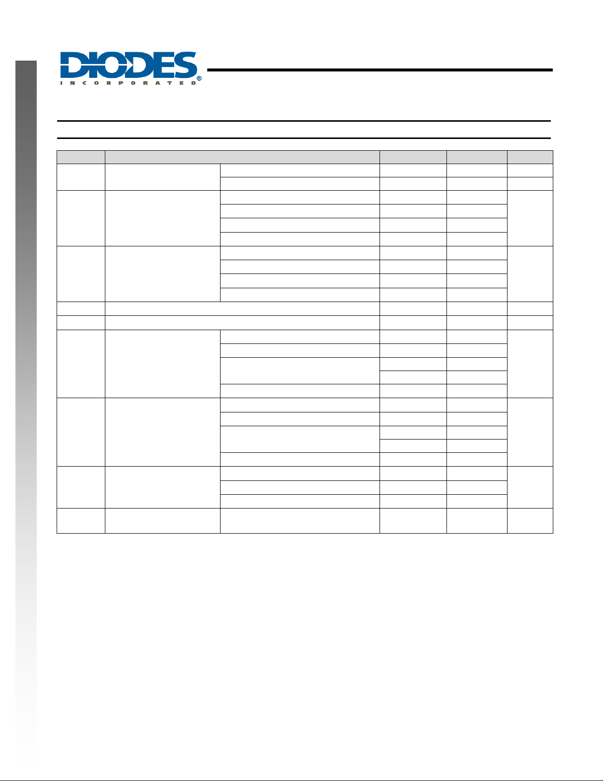
Recommended Operating Conditions (Note 3)
Symbol Parameter Min Max Unit
VCC
V
VIL
VI
VO
NEW PRODUCT
IOH
IOL
Δt/ΔV
TA
Notes: 3. Unused inputs should be held at Vcc or Ground.
Operating Voltage
High-level Input Voltage
IH
Low-level input voltage
Input Voltage 0 5.5 V
Output Voltage 0
High-level output current
Low-level output current
Input transition rise or fall
rate
Operating free-air
temperature
74LVC1G10
SINGLE 3 INPUT POSITIVE NAND GATE
Operating 1.65 5.5 V
Data retention only 1.5 V
V
= 1.65V to 1.95V 0.65 X VCC
CC
VCC = 2.3V to 2.7V
VCC = 3V to 3.6V
1.7
2
VCC = 4.5V to 5.5V 0.7 X VCC
VCC = 1.65V to 1.95V
VCC = 2.3V to 2.7V
VCC = 3V to 3.6V
VCC = 4.5V to 5.5V
= 1.65V
V
CC
VCC = 2.3V
VCC = 3V
VCC = 4.5V
= 1.65V
V
CC
VCC = 2.3V
VCC = 3V
VCC = 4.5V
V
= 1.8V ± 0.15V, 2.5V ± 0.2V
CC
VCC = 3.3V ± 0.3V
VCC = 5V ± 0.5V
0.7
0.8
-4
-8
-16
-24
-32
4
8
16
24
32
20
10
5
-40 125 ºC
0.35 X VCC
0.3 X VCC
VCC
V
V
V
mA
mA
ns/V
74LVC1G10
Document number: DS35121 Rev. 3 - 2
3 of 13
www.diodes.com
October 2011
© Diodes Incorporated

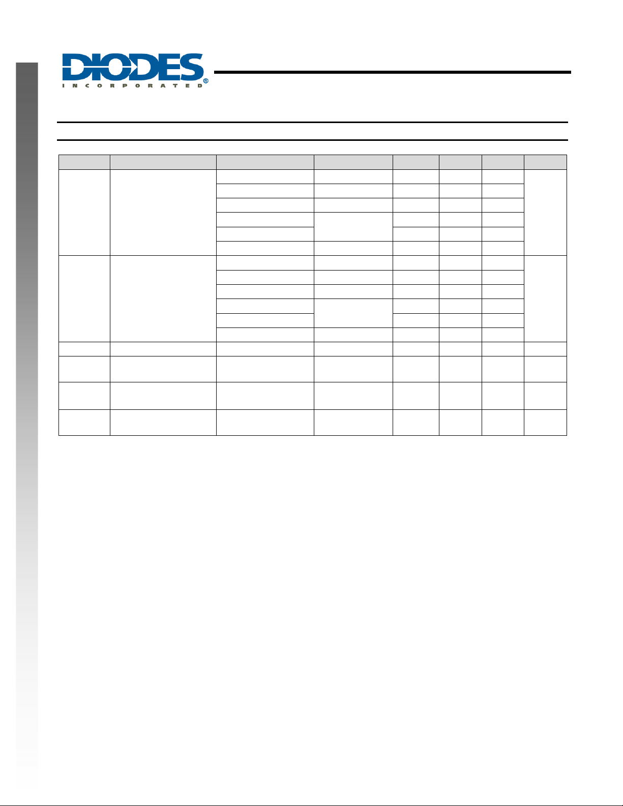
Electrical Characteristics T
Symbol Parameter Test Conditions
High Level Output
Voltage
High-level Input Voltage
II
Input Current
Power Down Leakage
Current
Supply Current
Additional Supply
Current
NEW PRODUCT
VOH
VOL
I
OFF
ICC
ΔICC
74LVC1G10
SINGLE 3 INPUT POSITIVE NAND GATE
= -40°C to 85°C (All typical values are at VCC = 3.3V, TA = 25°C)
A
Min Typ. Max Unit
V
– 0.1
CC
2.4
2.3
0.1
0.45
0.3
0.4
0.55
0.55
± 5 μA
10 μA
I
= -100μA
OH
IOH = -4mA
IOH = -8mA
IOH = -16mA
IOH = -24mA
IOH = -32mA
I
= 100μA
OL
IOL = 4mA
IOL = 8mA
IOL = 16mA
IOL = 24mA
IOL = 32mA
VI = 5.5 V or GND
or VO = 5.5V
V
I
= 5.5V of GND
V
I
=0
I
O
Input at V
–0.6V
CC
VCC
1.65V to 5.5V
1.65V 1.2
2.3V 1.9
3V
4.5V 3.8
1.65V to 5.5V
1.65V
2.3V
3V
4.5V
0 to 5.5V
0 ± 10 μA
1.65V to 5.5V
3V to 5.5V 500 μA
V
V
74LVC1G10
Document number: DS35121 Rev. 3 - 2
4 of 13
www.diodes.com
October 2011
© Diodes Incorporated
 Loading...