Diodes 74LVC06A User Manual

A
Description
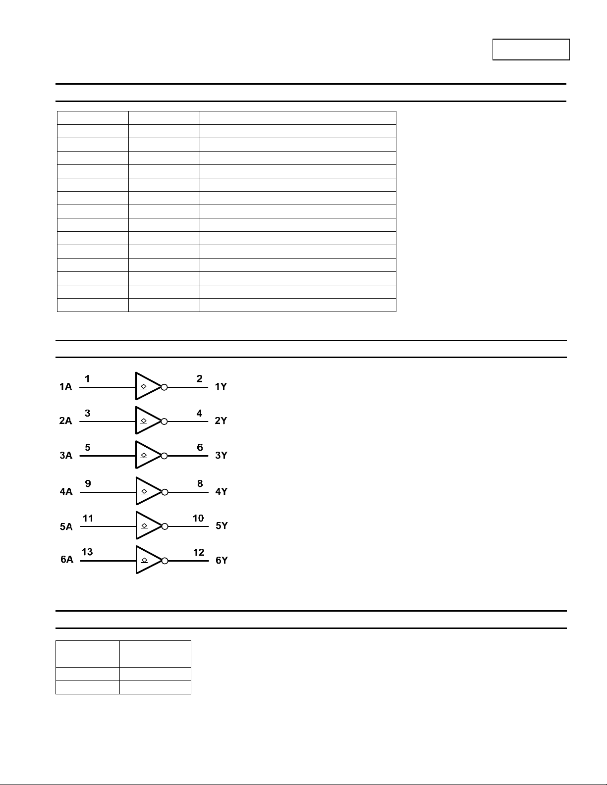
The 74LVC06A provides six independent open-drain inverter buffers.
The device is designed for operation with a power supply range of
1.65V to 5.5V. The inputs are tolerant to 5.5V allowing this device to
be used in a mixed voltage environment. The device is fully specified
for partial power down applications using IOFF. The IOFF circuitry
disables the output preventing damaging current backflow when the
device is powered down. The outputs can be connected to implement
active-low wired-OR or active-high wired-AND functions.
The gates perform the positive Boolean function:
AY =
74LVC06
HEX INVERTERS WITH OPEN DRAIN OUTPUTS
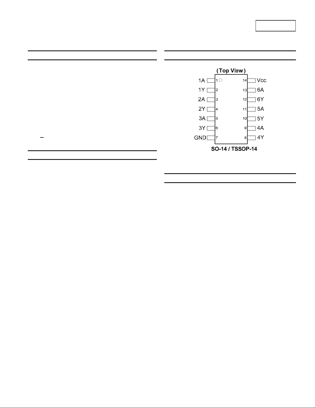
Pin Assignments
Features
• Wide Supply Voltage Range from 1.65V to 5.5V
• Sinks 24mA at V
• CMOS Low Power Consumption
• IOFF Supports Partial-Power-Down Mode Operation
• Inputs or Outputs Accept Up to 5.5V
• Inputs Can be Driven by 3.3V or 5.5V Allowing for Voltage
Translation Applications.
• ESD Protection Exceeds JESD 22
200-V Machine Model (A115-A)
2000-V Human Body Model (A114-A)
Exceeds 1000-V Charged Device Model (C101C)
• Latch-Up Exceeds 250mA per JESD 78, Class II
• Range of Package Options SO-14 and TSSOP-14
• Totally Lead-Free & Fully RoHS Compliant (Notes 1 & 2)
• Halogen and Antimony Free. “Green” Device (Note 3)
Notes: 1. No purposely added lead. Fully EU Directive 2002/95/EC (RoHS) & 2011/65/EU (RoHS 2) compliant.
2. See http://www.diodes.com for more information about Diodes Incorporated’s definitions of Halogen- and Antimony-free, "Green" and Lead-free.
3. Halogen- and Antimony-free "Green” products are defined as those which contain <900ppm bromine, <900ppm chlorine (<1500ppm total Br + Cl) and
<1000ppm antimony compounds.
74LVC06A
Document number: DS35259 Rev. 4 - 2
CC
= 3.3V
Applications
• Voltage Level Shifting
• General Purpose Logic
• Power Down Signal Isolation
• Wide array of products such as:
PCs, networking, notebooks, ultrabooks, netbooks
Computer peripherals, hard drives, CD/DVD ROM
TV, DVD, DVR, set top box
1 of 10
www.diodes.com
© Diodes Incorporated
July 2012

A
Pin Descriptions
Pin Number Pin Name Description
1 1A Data Input
2 1Y Data Output
3 2A Data Input
4 2Y Data Output
5 3A Data Input
6 3Y Data Output
7 GND Ground
8 4Y Data Output
9 4A Data Input
10 5Y Data Output
11 5A Data Input
12 6Y Data Output
13 6A Data Input
V
14
CC
Supply Voltage
Logic Diagram
74LVC06
Function Table
Inputs Outputs
A Y
H L
L Z
74LVC06A
Document number: DS35259 Rev. 4 - 2
2 of 10
www.diodes.com
July 2012
© Diodes Incorporated

A
74LVC06
Absolute Maximum Ratings (Note 4) (@T
Symbol Description Rating Unit
ESD HBM Human Body Model ESD Protection 2 KV
ESD CDM Charged Device Model ESD Protection 1 KV
ESD MM Machine Model ESD Protection 200 V
VCC
VI
VO Voltage applied to output in high impedance or I
VO
IIK Input Clamp Current VI < 0
IOK
IO
Continuous current through Vdd or GND ±100 mA
TJ
T
STG
P
TOT
Note: 4. Stresses beyond the absolute maximum may result in immediate failure or reduced reliability. These are stress values and device operation should
be within recommend values.
Supply Voltage Range -0.5 to +6.5 V
Input Voltage Range -0.5 to +6.5 V
Voltage applied to output in high or low state
Output Clamp Current V
Continuous Output Current 50 mA
Operating Junction Temperature -40 to +150 °C
Storage Temperature -65 to +150 °C
Total Power Dissipation 500 mW
< 0
O
Recommended Operating Conditions (Note 5) (@T
Symbol Parameter Conditions Min Max Unit
VCC
VI
VO
Δt/ΔV Input transition rise or fall rate
TA
Notes: 5. Unused inputs should be held at VCC or Ground.
Supply Voltage 1.65 5.5 V
Input Voltage 0 5.5 V
Output Voltage
Operating free-air temperature -40 +125 °C
Active Mode 0
V
CC
= 1.65V to 2.7V
V
CC
VCC = 2.7V to 5.5V
= +25°C, unless otherwise specified.)
A
state
OFF
= +25°C, unless otherwise specified.)
A
= 0V; Power Down Mode
-0.5 to +6.5 V
-0.3 to VCC +0.5
-50 mA
-50 mA
V
CC
0 5.5 V
20
10
V
V
ns/V
74LVC06A
Document number: DS35259 Rev. 4 - 2
3 of 10
www.diodes.com
July 2012
© Diodes Incorporated
 Loading...