Diodes 74HCT595 User Manual

74HCT595
8-BIT SHIFT REGISTER WITH 8-BIT OUTPUT REGISTER
Description
The 74HCT595 is an high speed CMOS device that is designed to
be pin compatable with 74LS low power Schottky types.
An eight bit shift register accpets data from the serial input (DS)
on each positive transition of the shift register clock (STCP).
When asserted low the reset function (MR
values to zero and is indepent of all clocks.
Data from the input serial shift register is placed in the output
register with a rising pulse on the storages resister clock (SHCP).
With the output enable (OE
Q7 become active and present th
All registers capture data on rising edge and change output on the
Preliminary
falling edge. If both clocks are connected together the input shift
register is always one clock cycle ahead of the output register.
Features
• Supply Voltage Range from 4.5V to 5.5V
• Sinks or sources 8mA at V
• CMOS low power consumption
• Schmitt Trigger Action at All Inputs
• Inputs accept up to 6.0V
• ESD Protection Tested per JESD 22
Exceeds 200-V Machine Model (A115-A)
Exceeds 2000-V Human Body Model (A114-A)
Exceeds 1000-V Charged Device Model (C101C)
• Latch-Up Exceeds 250mA per JESD 78, Class II
• Totally Lead-Free & Fully RoHS Compliant (Notes 1 & 2)
• Halogen and Antimony Free. “Green” Device (Note 3)
) sets all shift register
ሻ asserted low the 3-state outputs Q0-
= 4.5V
CC
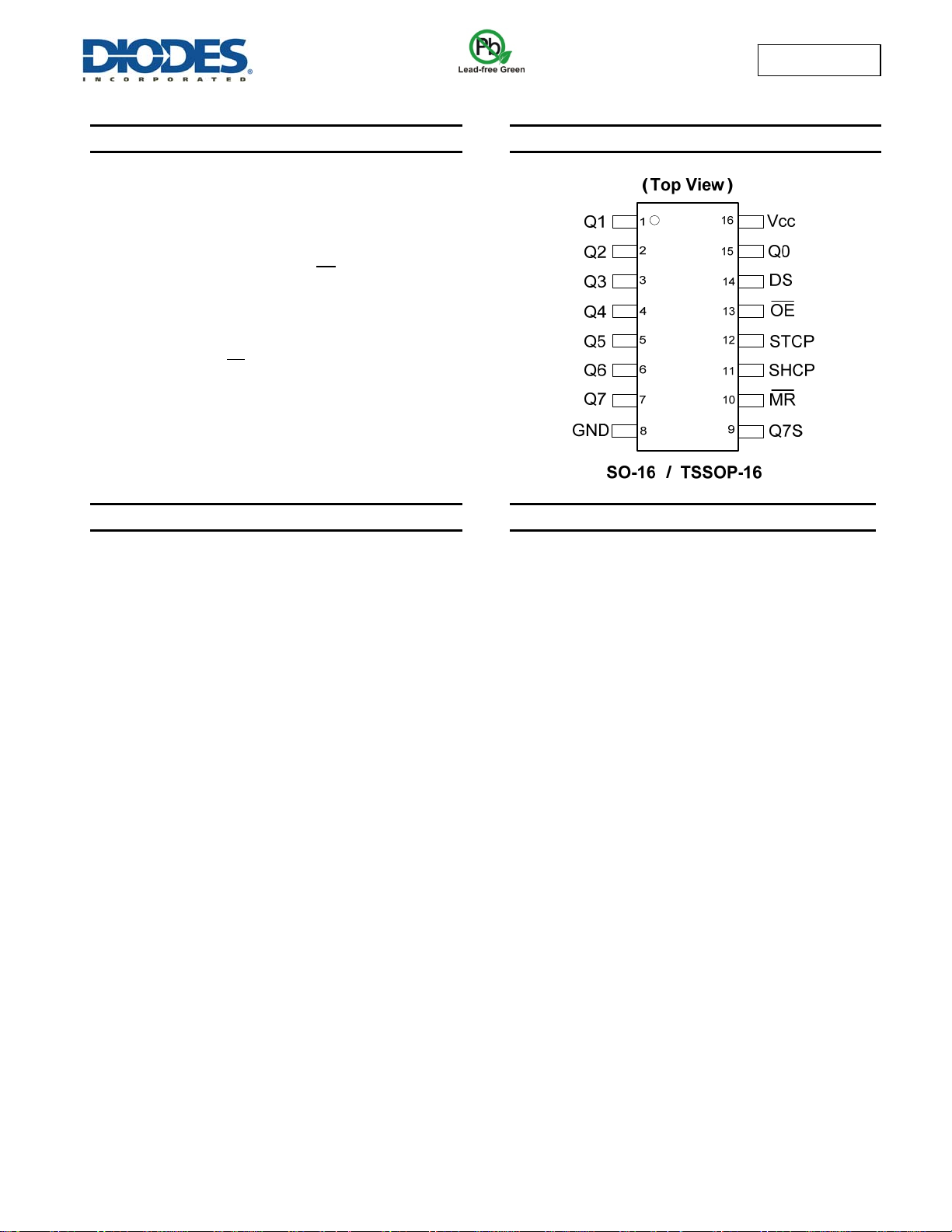
Pin Assignments
Applications
• General Purpose Logic
• Serial to Parallel Data conversion
• Capture and hold data for extended periods of time.
• Allow simple serial bit streams from a microcontroller to
control as many peripheral lines as needed.
• Wide array of products such as:
o Computer peripherals
o Appliances
o Industrial control
Notes: 1. No purposely added lead. Fully EU Directive 2002/95/EC (RoHS) & 2011/65/EU (RoHS 2) compliant.
2. See http://www.diodes.com/quality/lead_free.html for more information about Diodes Incorporated’s definitions of Halogen- and Antimony-free,
"Green" and Lead-free.
3. Halogen- and Antimony-free "Green” products are defined as those which contain <900ppm bromine, <900ppm chlorine (<1500ppm total Br + Cl)
and <1000 ppm antimony compounds.
Click for Ordering Information
74HCT595
Document number: DS35493 Rev. 3 - 2
1 of 11
www.diodes.com
July 2013
© Diodes Incorporated

Pin Descriptions
74HCT595
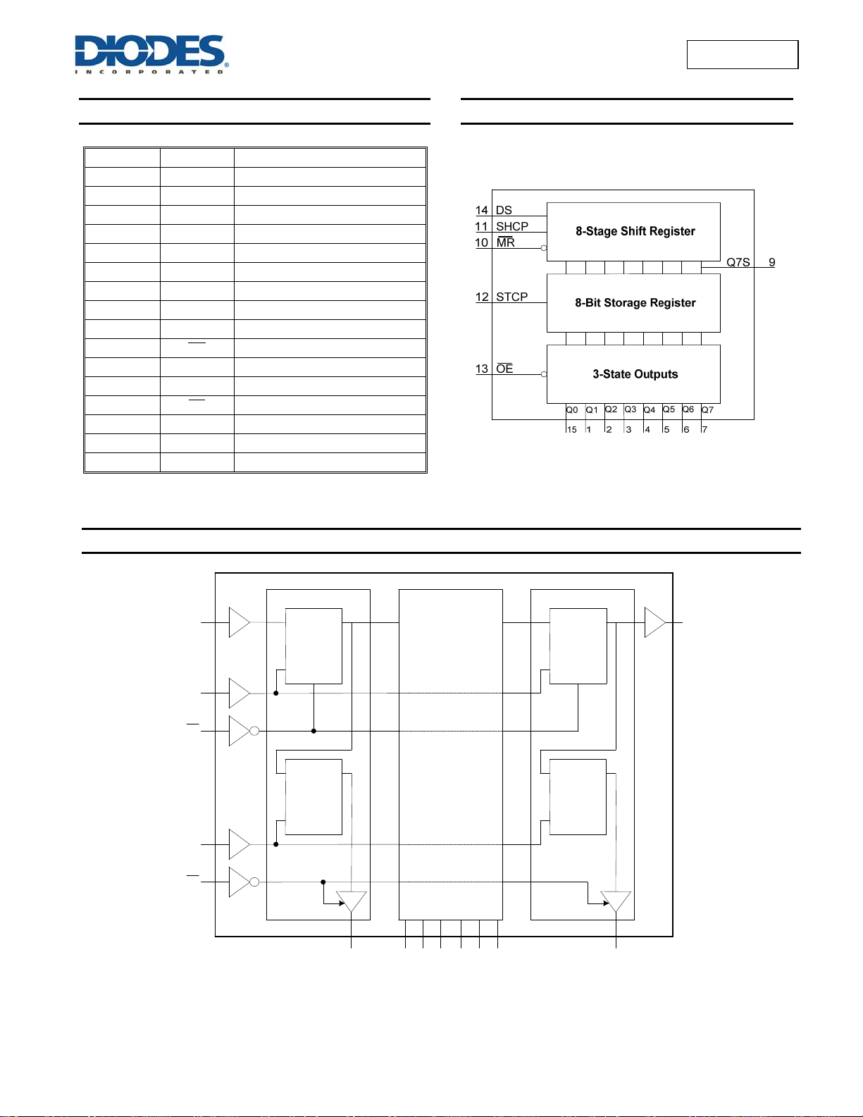
Functional Diagram
Pin Number Pin Name Description
1 Q1 Parallel Data Output 1
2 Q2 Parallel Data Output 2
3 Q3 Parallel Data Output 3
4 Q4 Parallel Data Output 4
5 Q5 Parallel Data Output 5
6 Q6 Parallel Data Output 6
7 Q7 Parallel Data Output 7
8 GND Ground
9 Q7S Serial Data Output
10 MR Master Reset Input
11 SHCP Shift Register Clock Input
12 STCP Storage Register Clock Input
Preliminary
13 OE Output Enable Input
14 DS Serial Data Input
15 Q0 Parallel Data Output 0
16 Vcc Supply Voltage
Logic Diagram
DS
SHCP
MR
STCP
OE
74HCT595
Document number: DS35493 Rev. 3 - 2
STAGE 0
DQ
FF0
CP
R
DQ
LATCH
CP
Q0
STAGES 1 TO 6
DQ
Q1 Q2
Q3Q5Q4
2 of 11
www.diodes.com
Q6
STAGE 7
DQ
FF7
CP
R
DQ
LATCH
CP
Q7
Q7S
July 2013
© Diodes Incorporated

74HCT595
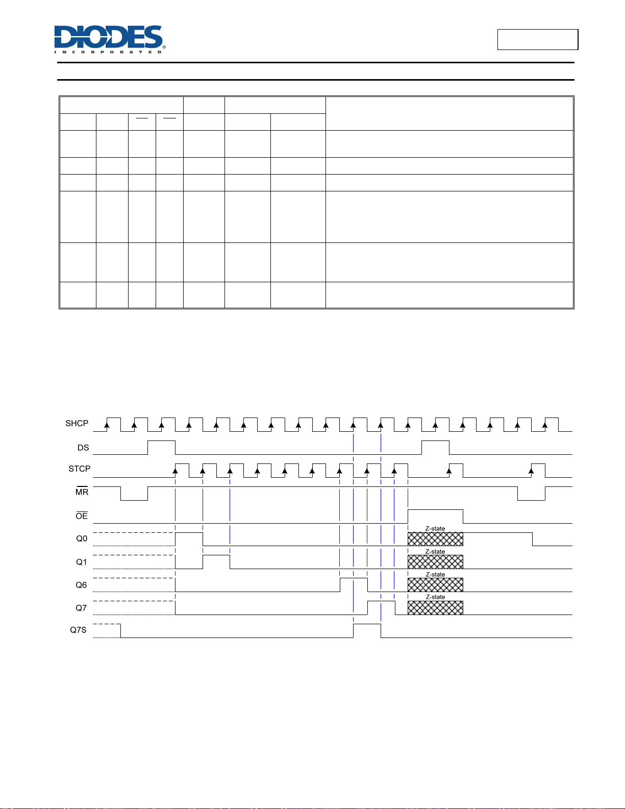
Functional Description and Timing Diagram
Control Input Output
SHCP STCP OE MR DS Q7S Qn
X X L L
X ↑ L L
X X H L
↑ X L H
X ↑ L H
Preliminary
↑ ↑ L H
H=HIGH voltage state
L=LOW voltage state
↑=LOW to HIGH transition
X= don’t care – high or low (not floating)
NC= No change
Z= high-impedance state
L NC
L L Empty shift register transferred to storage register
L Z Shift register remains clear; All Q ouputs in Z state
Q6S NC
NC QnS
Q6S QnS
Low-level asserted on MR clears shift register
Storage register is unchanged
HIGH is shifted into first stage of Shift Register Contents of each
register shifted to next register
The content of Q6S has been shifted to Q7S and now appears on
device pin Q7S
Contents of shift register copied to storage register
With output now in active state, the storage resister contents
appear on Q outputs
Contents of shift register copied to output register then shift register
shifted.
Function
74HCT595
Document number: DS35493 Rev. 3 - 2
3 of 11
www.diodes.com
July 2013
© Diodes Incorporated

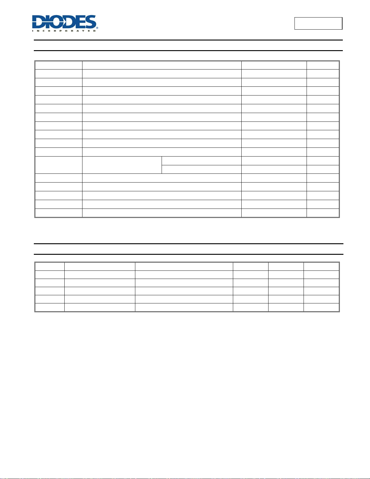
Absolute Maximum Ratings (Note 4) (@T
= +25°C°C, unless otherwise specified.)
A
Symbol Description Rating Unit
ESD HBM Human Body Model ESD Protection 2 kV
ESD CDM Charged Device Model ESD Protection 1 kV
ESD MM Machine Model ESD Protection 200 V
VCC
VI
Vo
IIK Input Clamp Current VI < -0.5V
IIK Input Clamp Current VI > Vcc +0.5V
IOK Output Clamp Current VO < -0.5V
IOK Output Clamp Current VO > VCC + 0.5V
IO
Preliminary
Note: 4. Stresses beyond the absolute maximum may result in immediate failure or reduced reliability. These are stress values, and device
operation should be within recommend values.
ICC Continuous current through VCC or GND
I
Continuous current through VCC or GND
GND
TJ
T
STG
P
TOT
Supply Voltage Range -0.5 to +7.0 V
Input Voltage Range -0.5 to +7.0 V
Voltage applied to output in high or low state
Continuous output current
Operating Junction Temperature -40 to +150 °C
Storage Temperature -65 to +150 °C
Total Power Dissipation 500 mW
Q7 standard output +/- 25 mA
Qn bus driver outputs +/- 35 mA
-0.3 to VCC +0.5
Recommended Operating Conditions (Note 5) (@T
= +25°C°C, unless otherwise specified.)
A
Symbol Parameter Conditions Min Max Unit
VCC
VI
VO
t/V Input transition rise or fall rate VCC = 4.5V to 5.5V
TA
Note: 5. Unused inputs should be held at Vcc or Ground.
74HCT595
Document number: DS35493 Rev. 3 - 2
Supply Voltage
Input Voltage
Output Voltage Active Mode 0
Operating free-air temperature
4 of 11
www.diodes.com
4.5 5.5 V
-40 125 °C
0 5.5 V
74HCT595
V
-20 mA
20 mA
-20 mA
20 mA
70 mA
-70 mA
VCC
100 ns/V
© Diodes Incorporated
V
July 2013
 Loading...