

Page 1
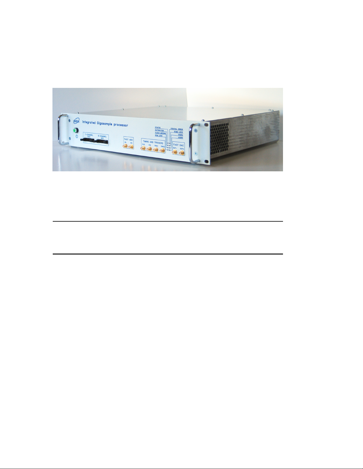
iGp-5120F Signal Processor
Technical User Manual
Author:
Dmitry Teytelman
September 19, 2008
Revision:
1.6
Page 2

dimtel
dimtel
Information in this document is subject to change without notice.
Copyright
Dimtel, Inc.
2059 Camden Avenue, Suite 136
San Jose, CA 95124
Phone: +1 650 862 8147
Fax: +1 603 907 0210
www.dimtel.com
©
Dimtel, Inc., 2007. All rights reserved.
Page 3

dimtel
dimtel
CONTENTS
Contents
1 Regulatory Compliance Information 3
2 Introduction 4
2.1 Delivery Checklist . . . . . . . . . . . . . . . . . . . . . . . . . 4
2.2 System Overview . . . . . . . . . . . . . . . . . . . . . . . . . 4
2.3 Front Panel Features . . . . . . . . . . . . . . . . . . . . . . . 6
2.4 Rear Panel Features . . . . . . . . . . . . . . . . . . . . . . . 8
2.5 Getting Started . . . . . . . . . . . . . . . . . . . . . . . . . . 9
3 IOC Setup 10
4 Utilities and Selftest 12
4.1 Utilities . . . . . . . . . . . . . . . . . . . . . . . . . . . . . . 12
4.2 Selftest . . . . . . . . . . . . . . . . . . . . . . . . . . . . . . . 13
5 User Interface 16
5.1 Installation . . . . . . . . . . . . . . . . . . . . . . . . . . . .
5.2 Starting the EDM . . . . . . . . . . . . . . . . . . . . . . . . . 17
5.3 Display Panels . . . . . . . . . . . . . . . . . . . . . . . . . . . 17
5.3.1 Main Panel . . . . . . . . . . . . . . . . . . . . . . . . 17
5.3.2 Control Panel . . . . . . . . . . . . . . . . . . . . . . . 18
5.3.3 Coefficients Panel . . . . . . . . . . . . . . . . . . . . . 21
5.3.4 Coefficient Generator Panel . . . . . . . . . . . . . . . 22
5.3.5 Timing Panel . . . . . . . . . . . . . . . . . . . . . . . 23
5.3.6 Drive Panel . . . . . . . . . . . . . . . . . . . . . . . . 25
5.3.7 Waveforms Panel . . . . . . . . . . . . . . . . . . . . . 27
5.3.8 Environmental Monitoring Panel . . . . . . . . . . . . 28
5.3.9 Device Controls Panel . . . . . . . . . . . . . . . . . . 29
5.3.10 8-channel ADC Panel . . . . . . . . . . . . . . . . . . . 31
5.3.11 GPIO Panels . . . . . . . . . . . . . . . . . . . . . . . 31
5.4 Power Amplifier Panel . . . . . . . . . . . . . . . . . . . . . . 34
16
6 External Software Interface 34
7 Specifications 36
1 of 58
Page 4

CONTENTS
dimtel
dimtel
8 Warranty and Support 40
8.1 Warranty . . . . . . . . . . . . . . . . . . . . . . . . . . . . .
8.2 Support . . . . . . . . . . . . . . . . . . . . . . . . . . . . . . 40
9 Appendix A: Address Map 41
9.1 Registers . . . . . . . . . . . . . . . . . . . . . . . . . . . . . . 41
9.1.1 Overall Layout . . . . . . . . . . . . . . . . . . . . . . 41
9.1.2 Gateware Config Register . . . . . . . . . . . . . . . . 42
9.2 Drive pattern memory . . . . . . . . . . . . . . . . . . . . . . 44
9.3 Environmental monitor . . . . . . . . . . . . . . . . . . . . . . 45
9.4 MAX1202 8-channel ADC . . . . . . . . . . . . . . . . . . . . 46
9.5 AD8842 8-channel DAC . . . . . . . . . . . . . . . . . . . . . 47
9.6 ECL delay lines . . . . . . . . . . . . . . . . . . . . . . . . . . 48
9.7 General-purpose digital I/O . . . . . . . . . . . . . . . . . . . 48
9.8 Memory . . . . . . . . . . . . . . . . . . . . . . . . . . . . . . 49
10 Appendix B: Connector Pinouts 50
40
11 Glossary 55
2 of 58
Page 5

dimtel
dimtel
Regulatory Compliance Information
1 Regulatory Compliance Information
This equipment requires a ground connection provided by the power source.
The exposed metal parts of the unit are connected to the power ground to
protect against electrical shock. Always use an outlet with properly connected protective ground.
iGp-5120F was designed and tested to operate safely under the following
environmental conditions:
indoor use;
altitude to 2000 meters;
temperatures from 5 to 40◦C;
maximum relative humidity 80% for temperature 31◦C, decreasing
linearly to 50% @ 40◦C;
pollution category II;
overvoltage category II;
mains supply variations of ±10% of nominal.
iGp-5120F contains no user serviceable parts inside. Do not operate with
the cover removed. Refer to qualified personnel for service.
NOTE: This equipment has been tested and found to comply with the limits
for a Class A digital device, pursuant to Part 15 of the FCC Rules. These
limits are designed to provide reasonable protection against harmful interference when the equipment is operated in a commercial environment. This
equipment generates, uses, and can radiate radio frequency energy and, if
not instal led and used in accordance with the instruction manual, may cause
harmful interference to radio communications. Operation of this equipment
in a residential area is likely to cause harmful interference in which case the
user will be required to correct the interference at his own expense.
NOTE: This Class A digital apparatus complies with Canadian ICES-003.
Cet appareil num´erique de la classe A est conforme `a la norme NMB-003 du
Canada.
3 of 58
Page 6
Introduction
dimtel
dimtel
ADC
Acquisition
memory
supply monitoring
Temperature and
Input
interface
USB
Output
RF clock
DACFPGA
Fiducial
Triggers
and digital I/O
Slow analog
USB driver EPICS IOC
Linux IOC
computer
Ethernet
2 Introduction
2.1 Delivery Checklist
1. iGp-5120F chassis;
2. AC power cord;
3. 16-pin ribbon cable;
4. 6 dB SMA attenuator;
5. 0.91 m SMA-to-SMA cable;
6. Compact disk with software and documentation;
7. User manual;
8. CE declaration of conformity.
2.2 System Overview
4 of 58
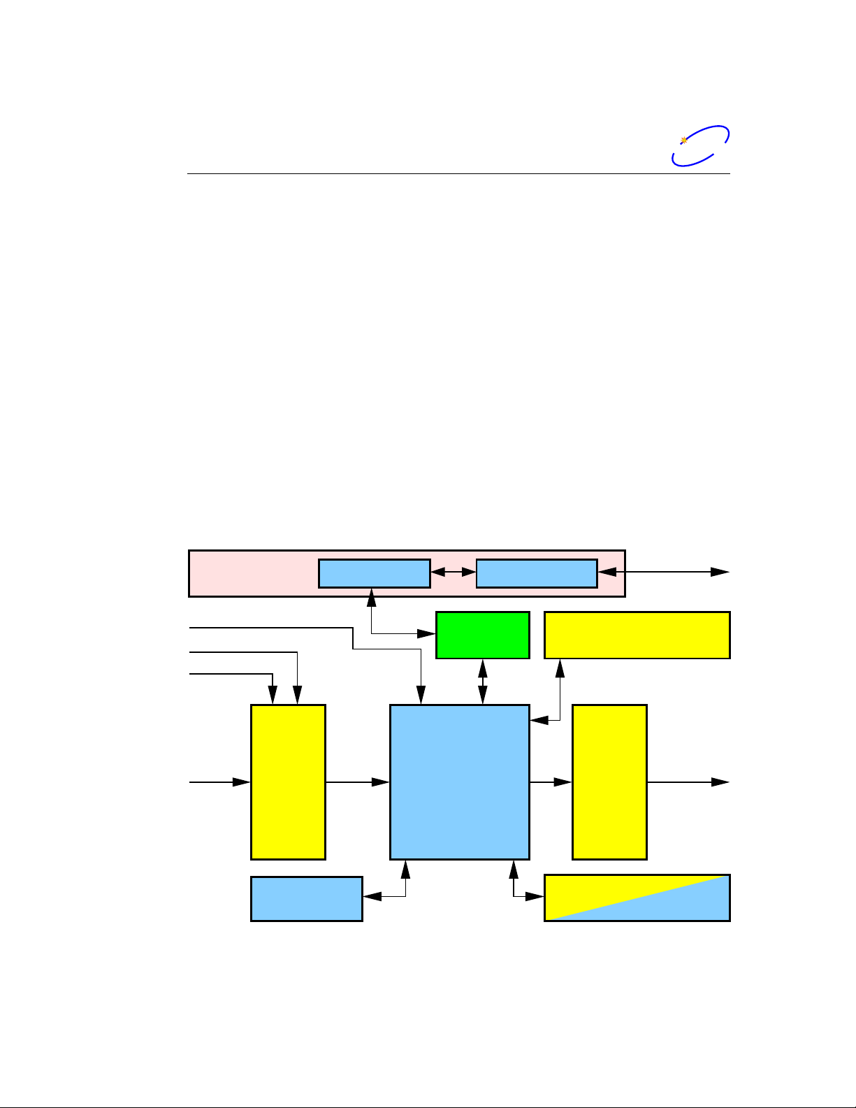
Figure 1: iGp-5120F blo ck diagram
Page 7

dimtel
dimtel
2.2 System Overview
iGp-5120F signal processor is designed for the bunch-by-bunch feedback
and diagnostics in lepton storage rings. Functionally iGp-5120F implements
a baseband bunch-by-bunch processing channel configured for 5120 bunches.
Each bunch is processed in a 8-tap finite impulse response (FIR) filter before
being s ent to the one-turn delay and, from there, to the high-speed digitalto-analog converter (DAC).
A block diagram of the iGp-5120F system is shown in Figure 1. The main
signal processing chain consists of a high-speed analog-to-digital converter
(ADC), a field programmable gate array (FPGA), and a high-speed DAC
and is driven by the radio frequency (RF) clock. In addition to performing
real-time control computations, the FPGA interfaces to a number of onboard devices, such as high-speed data acquisition memory (static random
access memory (SRAM)), low-speed analog and digital input/output (I/O),
as well as temperature and supply voltage monitors. In turn, the FPGA
uses an internal universal serial bus (USB) c onnection to communicate to
an embedded input-output controller (IOC) computer housed in the same
chassis. The IOC runs the Linux operating system and is connected to the
overall control system via the Ethernet.
5 of 58
Page 8
2.3 Front Panel Features
dimtel
dimtel
1 32 4 5 6 7 8 109
2.3 Front Panel Features
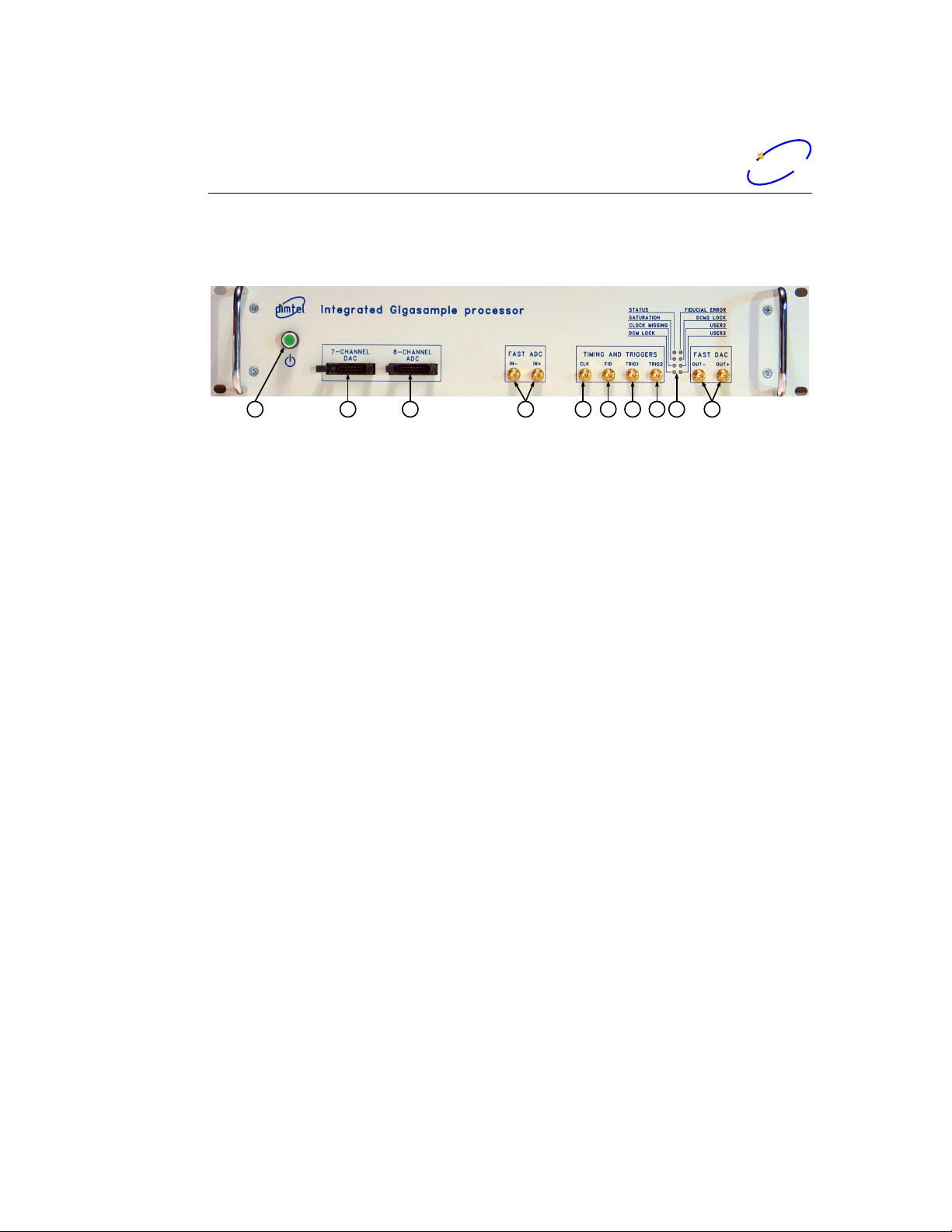
Figure 2: Front panel features
1) Power switch This momentary-on lighted switch turns iGp-5120F on
and off. From the off condition, the unit will take 25–30 seconds to fully
boot. Shutdown time after power switch actuation is 5–10 seconds.
2) Low-speed DAC This 16-pin connector provides 7 general-purpose analog outputs. DAC settings are adjustable via experimental physics and
industrial control system (EPICS).
3) Low-speed ADC This 16-pin input connector is provided for measuring
up to 8 external analog channels with 12-bit resolution.
4) Fast ADC Two SMA connectors accept the differential inputs for the
high-speed ADC. When a single input is used the full-scale (FS) swing
is 195 mV peak-to-peak. Differential mode swing is 97.5 mV peak-topeak.
5) RF Clock This input accepts the high stability bunch crossing clock signal (RF clock). Nominal input level is -3 dBm. The signal is internally
AC coupled.
6) Fiducial This input receives the revolution fiducial. Input is expected
to be NIM-level. Active edge is the 0 to −0.8 V transition. The signal
must be stable within one RF period for reliable operation.
7) Trigger 1 This input is currently unused.
8) Trigger 2 This NIM-level input is used as an external trigger for data
acquisition.
9) LEDs Eight front-panel LEDs provide indications of system activity and
operating status.
6 of 58
Page 9

dimtel
dimtel
2.3 Front Panel Features
STAT US FPGA Local bus activity is indicated in green.
SATURATION FIR filter operation status. Green indicates normal
operation, red — output saturation.
CLOCK MISSING Red indication when the input RF clock is not
detected.
DCM LOCK Lock status of the signal processing digital clock man-
ager (DCM). Green — locked, red — unlocked.
FIDUCIAL ERROR Red indication if the fiducial is missing, at the
wrong frequency, or jittering.
DCM2 LOCK (USER1) Lock status of the data acquisition DCM.
USER2 Data acquisition activity indicated in green.
USER3 Additional status of the signal processing DCM.
10) Fast DAC These two differential outputs are generated by the high-
speed DAC. For proper operation both outputs must be terminated
into 50 Ω.
7 of 58
Page 10
2.4 Rear Panel Features
dimtel
dimtel
1 32 4 5 6
2.4 Rear Panel Features
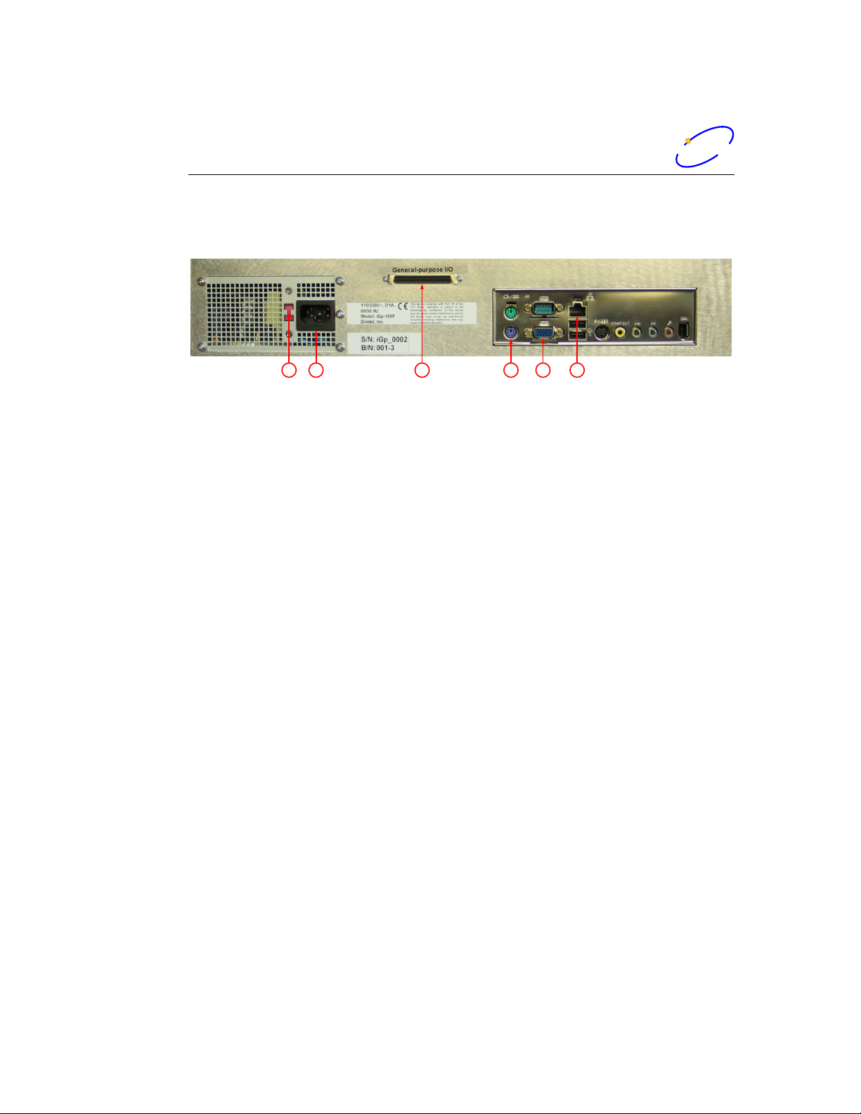
Figure 3: Rear panel features
1) Voltage selection switch Slide switch for selecting appropriate mains
voltage: 115 or 230 V.
2) Power entry socket IEC-320 power input socket. Always use an outlet
with properly connected protective ground.
3) GPIO This 68-pin connector provides 32 low-voltage transistor-transistor
logic (LVTTL) signals for future expansion.
4) PS/2 keyboard Connect PS/2 keyboard for the initial setup of the iGp5120F.
5) Monitor output Connect a monitor for the initial setup of the iGp5120F.
6) Network This RJ-45 connector is used to connect the iGp-5120F to the
control network. All control and data acquisition communications with
the unit are performed via this network connection.
8 of 58
Page 11

dimtel
dimtel
2.5 Getting Started
2.5 Getting Started
In this section we will present a quick step-by-step guide to get your new
feedback processor running in a minimal configuration.
WARNING: Before connecting power to the unit make sure the
voltage selection switch (Fig. 3, item 1) is in the correct positio n
(115 or 230 V).
1. Configure voltage selection switch (Fig. 3, item 1). Mains supply requirements for the iGp-5120F are listed in Table 8;
2. Connect RF clock at −3 dBm nominal level (Fig. 2, item 5);
3. Connect single-ended high-speed ADC input signal to Ain+ (Fig. 2,
item 4). The FS swing of this signal should be 190 mV peak-to-peak;
4. Connect a 50 Ω terminator to Ain- (Fig. 2, item 4);
5. Connect high-speed DAC output(s) (Fig. 2, item 10) to the appropriate
back-end unit;
6. If single-ended output configuration is used, connect a 50 Ω terminator
to the unused high-speed DAC output;
7. Connect a PS/2 keyboard (Fig. 3, item 4);
8. Connect a video monitor (Fig. 3, item 5);
9. Push the power button (Fig 2, item 1) to turn on the system;
10. Perform the IOC setup (see Chapter 3);
11. Push the power button (Fig 2, item 1) to turn the system off;
12. Disconnect the keyboard and the video monitor;
13. Connect the Ethernet (10/100BASE-T);
At this point your system is ready for internal testing and use in beam
diagnostics and feedback. To extend the configuration beyond the minimum
described above one can also connect the external fiducial and trigger signals
(NIM-level).
9 of 58
Page 12

IOC Setup
dimtel
dimtel
3 IOC Setup
Setup program is included in the IOC for configuring the important features
of the iGp-5120F. The program can be executed locally or remotely. For
local execution one must first connect a keyboard (Fig. 3, item 4) and a
video monitor (Fig. 3, item 5) to the system. For remote setup, use ssh
after system bootup to establish connection. In both setup methods the
user must login as root (initial password is supplied with the system). If the
newly received iGp-5120F must be configured remotely (when, for example, a
keyboard or a monitor is not available), such configuration can be performed
using a dedicated network. Set up a network consisting of the iGp-5120F, a
network hub or a switch, and a remote computer. The iGp-5120F is delivered
with the following network configuration:
IP address 192.168.1.41
Netmask 255.255.255.0
Gateway 192.168.1.254
Configure the remote computer as follows:
IP address 192.168.1.254
Netmask 255.255.255.0
Gateway 192.168.1.41
Once the dedicated network is configured, remote connection to the iGp5120F can be established by command ssh [email protected]. After logging in locally or remotely, start the setup program as follows:
[root@IOC ~]# setup
Setup program presents a series of text-mode window dialogs to collect the
necessary information for configuring the iGp-5120F. The following se ttings
are configured in this process: timezone, date, time, network, root password,
and EPICS device name.
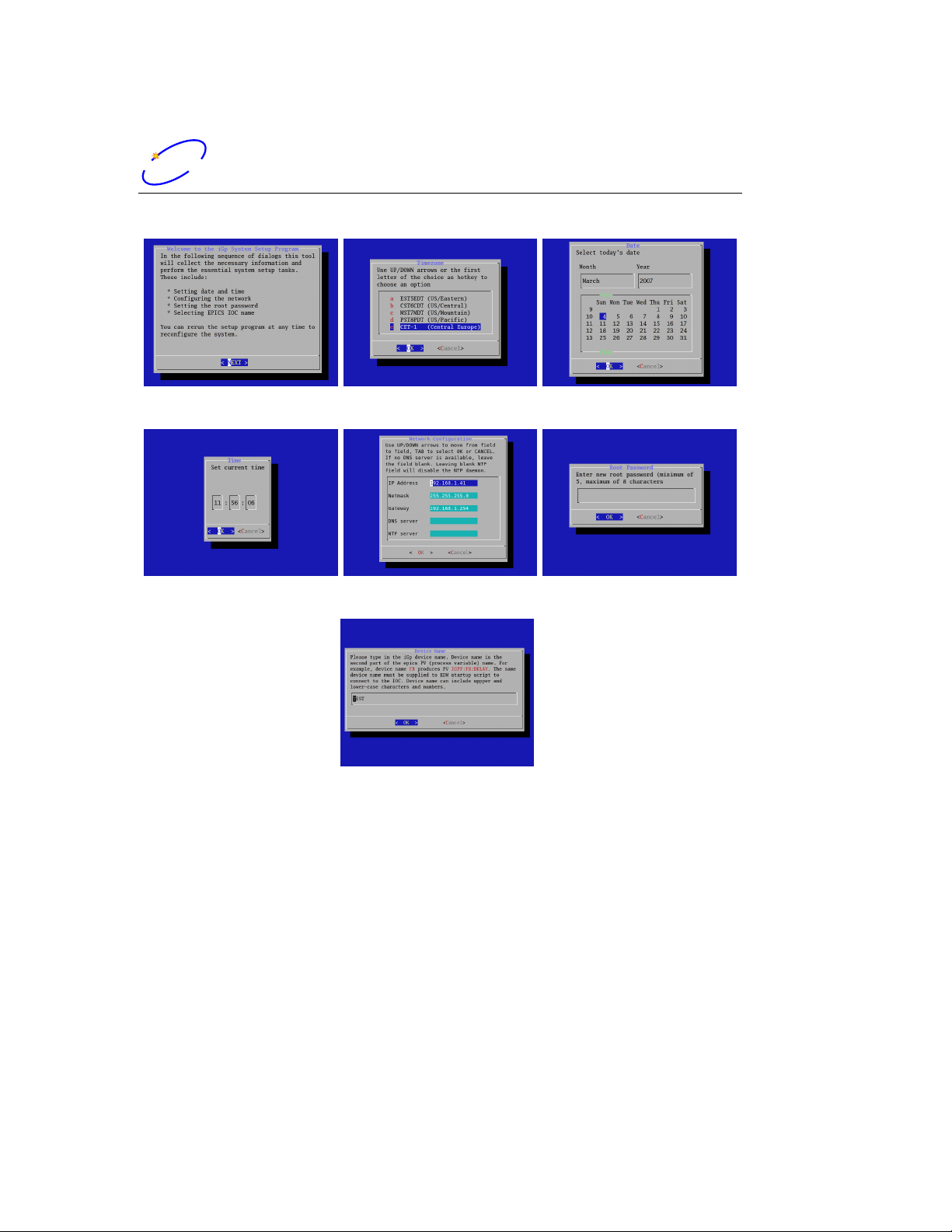
Setup dialogs are illustrated in Figure 4. Here we provide a step-by-step
guide through the setup process.
a) Welcome panel This panel provides a summary of settings handled by
the setup program.
10 of 58
Page 13
dimtel
dimtel
(a) Welcome screen (b) Timezone (c) Date
(d) Time (e) Network (f) Password
IOC Setup
(g) Device name
Figure 4: Setup screens
b) Timezone In this panel, select the appropriate timezone.
c) Date Set the correct date using the calendar.
d) Time Set the correct time. The initial setting is taken from the current
IOC time. If you know the current IOC time to be correct press OK
quickly to retain the setting as closely as possible.
e) Network Configure the IOC IP address, network mask and the default
gateway as provided by your network administrator. The DNS and
NTP server addresses are optional.
11 of 58
Page 14

Utilities and Selftest
dimtel
dimtel
NOTE: Only set the D NS address if the server connection is fast and
reliable. Delays in DNS server access can negatively impact the operation of the IOC.
f) Root password Type in the new root password. The password must 5
to 8 characters in length. Please use the standard rules for selecting a
strong password (Not based on a dictionary word, a mix of upper and
lower-case characters and numbers).
g) Device name This device name is the second part of the EPICS process
variable (PV). All PV names start with IGPF:X:, where X is the device
name. As delivered the iGp-5120F defaults to device name TEST producing PVs of the form IGPF:TEST:DELAY. If multiple iGp-5120F units
are to be deployed they must be assigned differing device names. For
example, one could use device names X, Y, Z for horizontal, vertical,
and longitudinal feedback channels.
NOTE: If the setup program is executed remotely and the network address is
changed, the ssh connection will hang at the end of the process. To connect
to the IOC, close the existing ssh session and start the new connection at
the newly assigned IOC IP address.
4 Utilities and Selftest
4.1 Utilities
The IOC includes several utilities designed to communicate to the iGp-5120F
directly, without using the EPICS softIOC software. These utilites allow the
user to access individual FPGA registers and memory locations. For register
descriptions and address map see Sec. 9. All of the utilities below will accept
addresses and data in decimal, hex, if preceded by 0x, and octal, if the value
starts from 0. For example, value 12 can be specified as 12, 0xc, 014. In
order for these utilities to gain access to the FPGA interface the IOC process
must be terminated. To terminate the IOC execute:
[root@IOC ~]# pkill st.cmd
Here is a short description of the available commands:
usbr <addr> Read a single register or memory location.
12 of 58
Page 15

dimtel
dimtel
4.2 Selftest
usbw <addr> <val> Write a single location.
usbrblk <addr> <len> Read a block of memory. The data is send to
stdout and can be redirected into a file.
usbwblk <addr> <len> Write a block of memory. This utility expects the
data from stdin.
usbtest <addr> <len> <cnt> Test the register or memory block specified
by the addr,len combination. The utility generates a block of random
numbers and writes it to the FPGA. Then the data is read back and
compared to the original values. Argument cnt specifies the number
of test cycles to perform.
4.2 Selftest
Another important utility included in the IOC is selftest. This program
performs testing of the main signal path, memories, and peripherals. In order
to perform the testing system hardware must be configured as follows:
Connect the 16-pin ribbon cable between the 7-channel DAC (Fig. 2,
item 2) and the 8-channel ADC (Fig. 2, item 3);
Connect 509 MHz clock to the RF clock input (Fig. 2, item 5);
Terminate Ain- fast ADC input (Fig. 2, item 4);
Terminate Aout- fast DAC output (Fig. 2, item 10);
Connect 6 dB attenuator to Aout+ fast DAC output;
Connect the output of the attenuator to Ain+ fast ADC input using
the supplied SMA-SMA cable;
Make sure no cable is connected to the general-purpose digital I/O port
(Fig. 3, item 3);
Make sure fiducial input is not driven (Fig. 2, item 6);
Once the hardware is configured the test procedure can be initiated by
typing selftest at the IOC command prompt (establish local or remote
connection to the IOC as described in Sec. 3). Example output of the test is
shown below:
13 of 58
Page 16

4.2 Selftest
dimtel
dimtel
1 T e rmi n ati n g the IOC
2
3 Sys tem i n f o r m at i o n :
4 Fun c tio n : fe ed ba ck
5 Harmo nic number : 64
6 D e m u l t ip le xi ng : 4
7 R ev is i o n : 1 . 01
8 S e r i a l number : iGp 0003
9
10 STARTING THE AUTOMATED TEST SEQUENCE
11
12 T e s t i ng i n t e r n a l blockRAM : [OK]
13 T e s t i ng ex t e r n a l SRAM: [OK]
14 T e s t i ng ge n er al −p urp ose d i g i t a l in pu t s / ou tp u ts : [OK]
15 Ve r i f y i n g RF c l o c k pr es e n c e and DCM l oc k : [OK]
16
17 T e s t i ng low−sp eed DAC/ADC sy s tem
18 Ch(ADC) ADC(mV) DAC(mV) O ff (mV) DAC(mV) ADC(mV)
19 1 −2040 −2 062 5 2039 2025
20 2 −2024 −2 039 −4 2039 2028
21 3 −2035 −2 039 −3 2039 2033
22 4 −2029 −2 039 2 2039 2035
23 5 −2025 −2 039 8 2039 2030
24 6 −2033 −2 039 −3 2039 2034
25 7 −2031 −2 039 −3 2039 2035
26
27 T e s t i ng hi g h −sp e ed DAC o f f s e t ch a nn el
28 O f f s e t DAC( cn t ) Fa s t ADC( cn t )
29 −128 − 17.3
30 66 1 . 0
31 127 6 .9
32
33 T e s t i ng hi g h −sp e ed DAC ou t put
34 HS DAC( c nt ) HS ADC( cn t )
35 −1574 − 1 2 0.0
36 0 −0.0
37 15 7 6 1 20 .0
38
39 E n viro n men t al m ea su r em en ts
40 Bul k su pp l y v o l t a g e ( 12V ) : 12 . 0
41 Vcc sup pl y vo lt a g e ( 3 . 3V ) : 3 . 3
42 FPGA c or e s u pp l y v o l t a ge ( 1 . 5V ) : 1 . 5
43 iGp board te mpe ra t ur e ( deg C ) : 25 . 7
44 ADC t emp er a tu r e r i s e ( d e g C ) : 50 . 4
45 FPGA te mpe ra t ur e r i s e ( deg C) : −0.3
14 of 58
Page 17

dimtel
dimtel
4.2 Selftest
46 FID c l o c k de l a y t e mp e ra tur e r i s e ( deg C) : 5 . 8
47 DAC cl o ck del ay t emp er a tu r e r i s e ( d e g C ) : 6. 1
Line 1 The utility terminates the IOC process to gain access to the FPGA
interface.
Lines 3–8 Contents of the FPGA config register are parsed and printed out.
Line 12 Test of the data acquisition blockRAM.
Line 13 External SRAM test.
Line 14 General-purpose digital I/O is tested.
Line 15 Presence of the RF clock is verified as well as the lock status of the
DCMs.
Lines 17–25 A test of the low-speed DAC and ADC system. This test
uses 7 channels of the DAC to drive different voltages and measures
the voltages using the ADC. The test measures several parameters for
each channel. Test code finds the minimum DAC setting that does not
saturate the ADC. ADC reading (column 2) and the dead-reckoned
DAC output (column 3) are printed out in millivolts. Next the DAC is
set to 0 and the ADC reading (offset, column 4) is taken. Finally, the
code finds the maximum DAC setting that does not saturate the ADC.
Lines 27–31 This portion of the test uses channel 7 of the slow DAC to
adjust the output offset of the high-speed DAC˙The code extracts the
reading from the high-speed ADC at the positive and negative extremes
of the offset DAC. Next the code finds the offset DAC setting that
minimizes the high-speed ADC measurement. This setting should be
very close to the factory determined value used in EPICS to null the
high-speed DAC output.
Lines 33–37 This fragment verifies the response via the high-speed DAC.
To do so it finds the DAC settings to obtain readings of ±120 and 0
counts from the ADC.
Lines 39–47 Environmental monitor readings are taken and displayed.
The output of selftest utility can be redirected to a file and compared
to the factory measurement provided in /root/factory.selftest.
After testing restart the IOC process by typing:
[root@IOC ~]# iGp_start
15 of 58
Page 18

User Interface
dimtel
dimtel
5 User Interface
User interface functionality for the iGp-5120F is implemented using extensible display manager (EDM). Software installation CD is designed for seamless
installation on a client computer, configured with Fedora 8 version of Linux
operating system.
5.1 Installation
Log into the client computer.
Insert the installation CD into the CD-ROM drive.
Mount the CD by accepting the ”Open in New Window” option or by
right clicking on the CD icon and selecting ”Mount”.
Open a terminal window.
Issue the following installation command:
sudo sh <CD mount point>/install.sh. Typically CD mount point
will be /media/iGp. Note: to install the software one must have supe-
ruser privileges, obtained either via sudo or su.
When prompted, enter the user name to install under. If the specified
user does not exist it will be created. Default user name is iGp.
When prompted, enter the installation directory. Default directory is
iGp.
If the specified user did not exist, the program will prompt for password.
Wait for the installation process to complete.
The resultant installation can support multiple IOCs with distinct device
names. Refer to Section 3 for a definition of the device name. Each IOC
must be added to the configuration. To to so, log in under the username,
specified during software installation (EPICS user). Open a terminal and
type:
[iGp@host ~]$ IOC_add <IP address> <device name>
WARNING: IOC and the client computer must be able to communicate at this point, otherwise IOC add will fail.
After adding one or more new IOCs to the c onfiguration the user must
log out and log back in for the changes to take effect.
16 of 58
Page 19
dimtel
dimtel
5.2 Starting the EDM
5.2 Starting the EDM
Once the software has been installed and the IOCs added via IOC add you
are ready to start the EDM. iGp-5120F display panels are opened by the
following command:
[iGp@host ~]$ iGp_display [device name]
Note that the device name is optional. If the argument is omitted the command defaults to device name TEST.
5.3 Display Panels
5.3.1 Main Panel
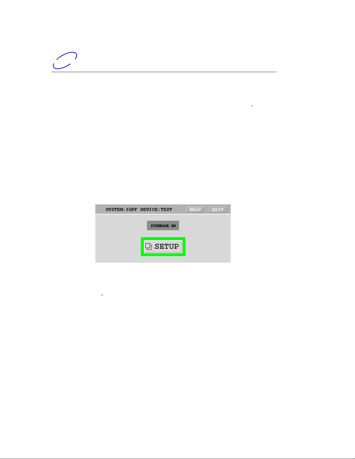
Figure 5: Main (top-level) panel
Running iGp display brings up the top-level panel shown in Figure 5.
All of the display panels include two buttons on the top: HELP and EXIT.
EXIT button will always c lose the current window. In addition, EXIT button
on the top-level panel will close the EDM session.
Top-level panel consists of three elements: FEEDBACK ON/OFF control, SETUP button and the status border around this button. The FEED-
BACK ON/OFF control enables or disables the FIR filter output to the DAC.
The status border indicates system operational status summary. Green indicates no errors, yellow - warning (saturation), red - error. The SETUP
button opens the control panel shown in Fig. 6.
17 of 58
Page 20
5.3 Display Panels
dimtel
dimtel
5.3.2 Control Panel
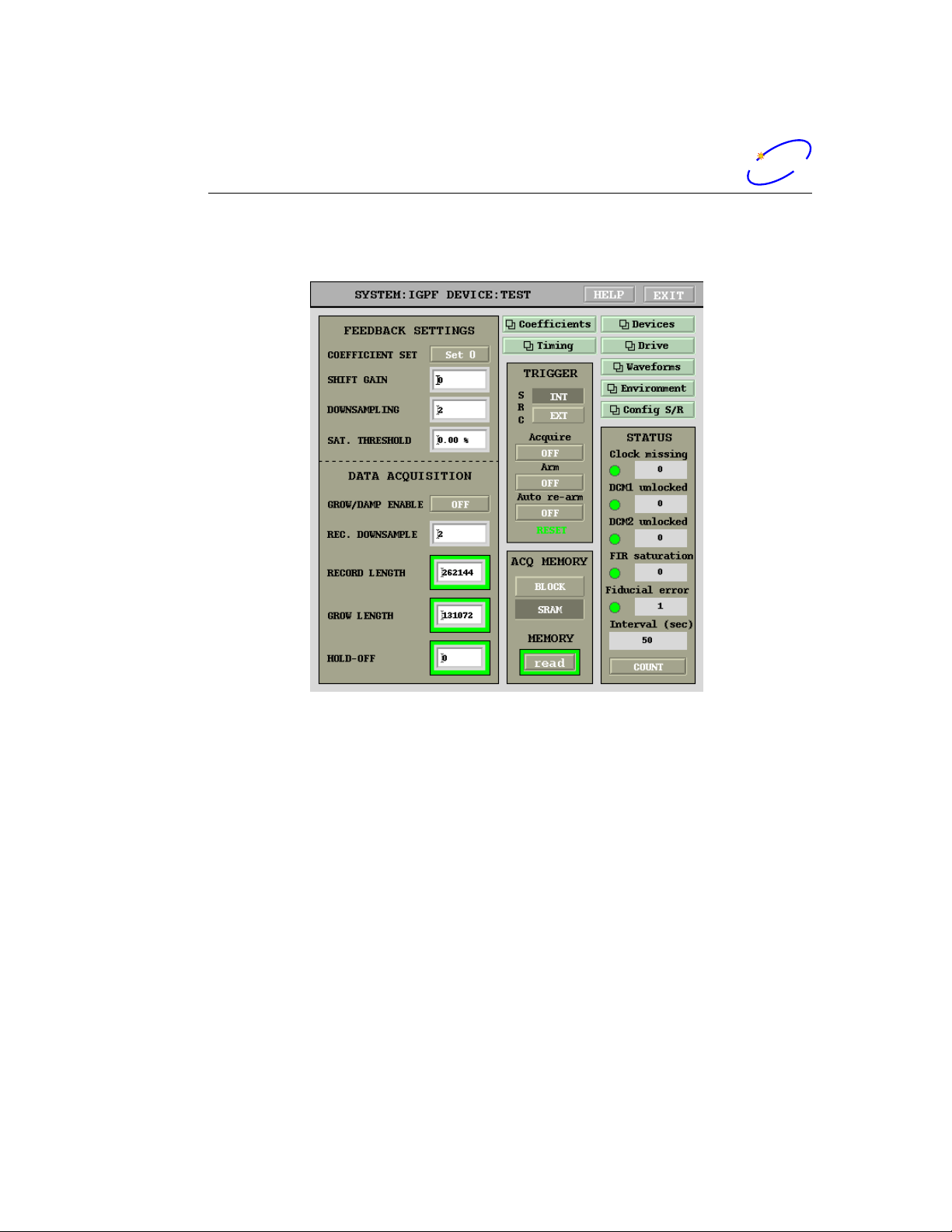
Figure 6: Control panel
This window integrates most important controls for the iGp-5120F.
COEFFICIENT SET Feedback coefficient set selector.
SHIFT GAIN Output gain adjustment, each step doubles the feedback
gain.
DOWNSAMPLING Processing channel downsampling factor.
SAT. THRESHOLD iGp-5120F is equipped with an integrating satura-
tion counter. The counter is compared with a threshold duty cycle,
expressed here in percent. A setting of 50% indicates that the output
was saturated half the time. On every poll cycle (once a second) the
threshold comparison result is read out and the counter is reset to 0.
Value of 0 produces single saturation event detector within a polling
period,
18 of 58
Page 21

dimtel
dimtel
5.3 Display Panels
GROW/DAMP ENABLE Enables coefficient set switching during data
acquisition.
REC. DOWNSAMPLE Acquisition channel downsampling factor. This
downsampling process is completely decoupled form the processing
channel downsampling.
RECORD LENGTH Number of samples to acquire during data acquisi-
tion. The value is limited to 131072 for blockRAM and 8388608 for
SRAM. Lengths up to 524288 will be read out every second. Longer
acquisition lengths will require multiple poll periods to read out.
GROW LENGTH Number of samples to hold the coefficient set select
inverted during data acquisition.
HOLD-OFF Number of groups of 4 samples to keep the coefficient set
select inve rted before data acquisition. This can be used to delay data
acquisition and give slow oscillations time to grow.
TRIGGER SRC Acquisition trigger source, internal or external. External
trigger is taken from TRIG2 input (NIM-level).
Acquire Acquisition trigger pushbutton for internal trigger. This control is
no longer actively used - see the waveform panel (Fig. 11).
Arm External trigger is only valid if the acquisition system is armed. Single-
event acquisitions on the external trigger can be performed by pushing
this button.
Auto re-arm This option re-arms the acquisition system after each data
readout. This allows for continuous updates of beam data triggered by
external signal.
ACQ MEMORY Selects which memory, FPGA blockRAM or SRAM is
used for acquisition.
MEMORY read Reads out the results of the last acquisition and places
them in a file on the IOC.
Coefficients Opens FIR coefficients control panel.
Timing Opens timing control panel.
19 of 58
Page 22

5.3 Display Panels
dimtel
dimtel
Devices Opens the control panel for the integrated devices.
Drive Opens the drive control panel.
Waveforms Opens the data acquisition and display panel.
Environment Opens the environmental monitoring panel.
Config S/R Configuration save/restore panel.
Clock missing RF clock missing indicator.
DCM1 unlocked Signal processing DCM lock indicator.
DCM2 unlocked Data acquisition DCM lock indicator.
FIR saturation FIR filter output saturation duty cycle exceeds the thresh-
old level.
Fiducial error Indicates missing or jittering fiducial.
Interval Number of polling cycles (seconds) since the last error counter
reset.
COUNT Reset error and interval counters.
20 of 58
Page 23
dimtel
dimtel
5.3.3 Coefficients Panel
5.3 Display Panels
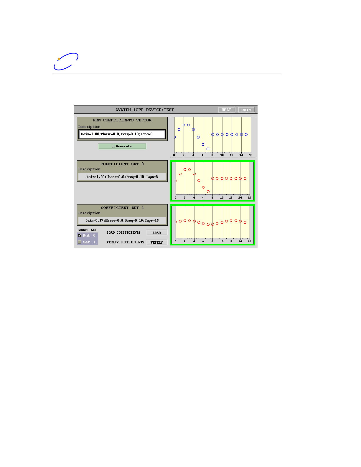
Figure 7: Co efficients panel
Coefficients control panel allows the user to manipulate the loaded coefficients sets and verify that the hardware is in sync with the panel display.
The panel is split into three functional groups: new coefficients vector, coefficient set 0, and coefficient set 1. The first group shows the coefficient vector
and its description generated using coefficient generator panel (Fig. 8). This
vector can be loaded into hardware coefficient sets 0 or 1. Colored borders
around the hardware coefficient displays indicate the results of coefficient
verification. Green shows that the readback is in agreement with the EPICS
values.
Generate Opens the coefficient generator panel.
TARGET SET Selects which set the new coefficient vector is to be loaded.
LOAD COEFFICIENTS Loads the new vector to the hardware coeffi-
cient set specified by TARGET SET.
VERIFY Verifies coefficient sets 0 and 1 against hardware values.
21 of 58
Page 24
5.3 Display Panels
dimtel
dimtel
5.3.4 Coefficient Generator Panel
Figure 8: Co efficient generator panel
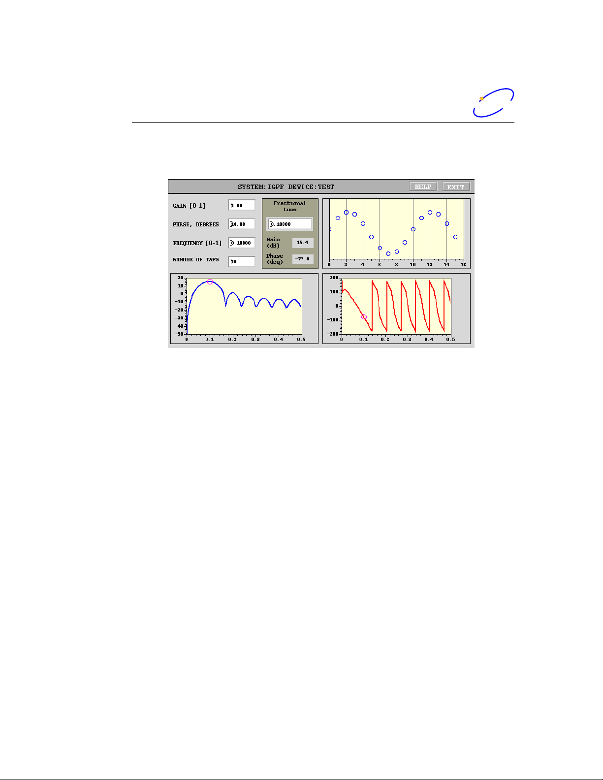
Coefficient generator panel shown in Figure 8 allows the user to generate
feedback processing controllers and explore different delay/gain/bandwidth
tradeoffs. This tool generates a coefficient set based on sampling a sine
wave. Transfer function of the filter is computed and displayed together with
a adjustable marker.
GAIN Filter gain in the range from 0 to 1.
PHASE Filter phase in degrees.
FREQUENCY Center frequency in fractional tune units. Multiply this by
the revolution frequency to get the physical center frequency.
NUMBER OF TAPS Number of filter taps.
Fractional tune Marker frequency.
Gain (dB) Gain at the marker frequency in dB.
Phase (deg) Phase at the marker frequency in degrees.
22 of 58
Page 25
dimtel
dimtel
5.3 Display Panels
5.3.5 Timing Panel
Figure 9: Timing panel
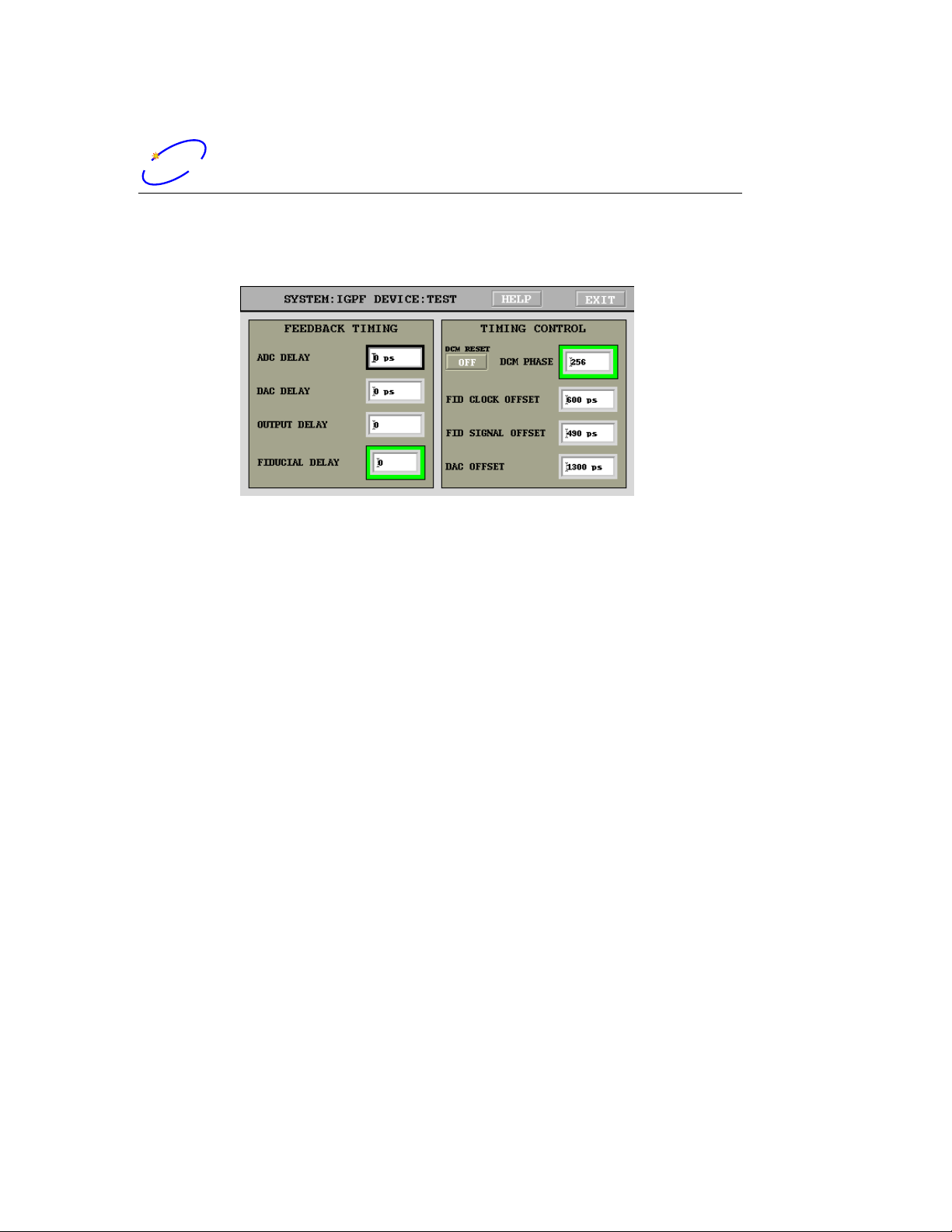
This window provides controls for system timing.
ADC delay High-speed ADC clock delay in picoseconds. T his adjustment
is independent of the back-end timing (DAC delay) and has a range
from 0 to Trf− 1 ps. Rounding to 10 ps adjustment step size is handled
automatically.
DAC delay High-speed DAC clock delay in picoseconds. This adjustment
is independent of the front-end timing (ADC delay) and has a range
from 0 to Trf− 1 ps. Rounding to 10 ps adjustment step size is handled
automatically.
OUTPUT DELAY High-speed DAC output delay in units of RF periods.
FIDUCIAL DELAY Input fiducial delay in steps of two bunches. Use to
place bunch 1 signal in channel 1 of the data acquisition. For example,
if bunch 1 signal is seen in acquisition channel 3, increment this field
by 1. Fiducial delay of one bunch can be achieved by adjusting FID
SIGNAL OFFSET by one RF period.
DCM RESET Pushbutton for resetting feedback processing DCM (DCM1)
and data acquisition DCM (DCM2). Push this button if DCM unlocked
indicators are red and the RF clock is present at the iGp-5120F front
panel. On rare occasions due to intermittent RF clock loss DCM might
need to be reset even though lock indicators are green.
23 of 58
Page 26

5.3 Display Panels
dimtel
dimtel
DCM PHASE ADC data acquisition phasing. This parameter is config-
ured at the factory and does not need to be adjusted in operation.
FID CLOCK OFFSET Offset between the ADC clock and the fiducial
clock. This parameter is configured at the factory and does not need
to be adjusted in operation.
FID SIGNAL OFFSET This offset sets the relative timing of the input
fiducial signal and the fiducial receiving clock. This setting must be
optimized after installation. To do so, connect the RF clock and the
fiducial in the final (operational) configuration. Then, adjust the fiducial delay to find the error range. Let us consider, for example, RF
frequency of 368 MHz. The RF period is 2700 ps. Within one period
there should be a range of delays in which the fiducial is jittering across
the RF clock and the fiducial error indicator is red. By moving the delay in steps of 100 ps find the beginning (N1) and the end (N2) of this
range. The optimal setting is at (N1+ N2)/2 ± 1350 ps.
DAC OFFSET Offset between FPGA data and DAC clock. This param-
eter is configured at the factory and does not need to be adjusted in
operation.
24 of 58
Page 27
dimtel
dimtel
5.3.6 Drive Panel
5.3 Display Panels
Figure 10: Drive panel
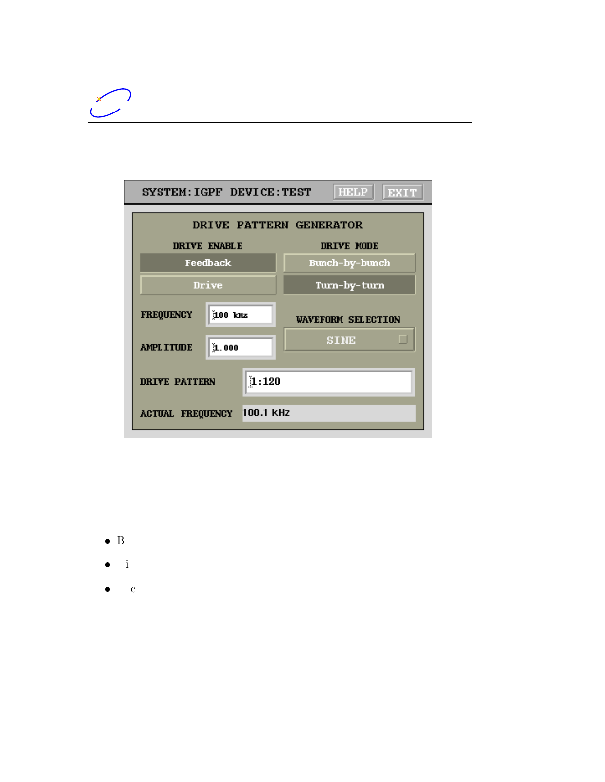
Drive panel shown in Figure 10 provides the means to generate an arbitrary waveform on a bunch-by-bunch basis. The drive output has many
applications:
Back-end timing;
Kicker gain checking;
Excitation source for front-end timing;
DRIVE ENABLE Switches high-speed DAC between the feedback filter
output and the drive signal.
DRIVE MODE In the bunch-by-bunch mode the waveform memory ad-
dress is updated every RF clock. In this mode the highest output
frequency is Frf/2. In the turn-by-turn mode the memory address is
25 of 58
Page 28

5.3 Display Panels
dimtel
dimtel
updated every turn. Consequently, the highest output frequency is
F
/2 with significantly better frequency resolution.
rev
FREQUENCY Drive frequency in Hz.
AMPLITUDE Drive amplitude in the range from 0 to 1.
WAVEFORM SELECTION Waveform se lector allows the user to drive
the beam with sine, square, sawtooth, and arbitrary signals. Arbitrary
signal selection loads the drive memory with a signal from the waveform
PV$(SYS):$(DEV):DRIVE:ARB.
DRIVE PATTERN Drive pattern string selects bunches to be driven.
The syntactic structure of this field allows three types of elements:
single bunch number, range, range with a step. Individual elements
should be separated by spaces. Single bunch number element is an integer in the range from 1 to 5120. A range is specified as start:stop.
Range can wrap around, that is if stop is smaller than start the
range covers 1:stop start:5120. To specify a range with a step use
start:step:stop construct. For example, drive pattern of [2:2:5120
1:10 13] includes all even bunches, range from 1 to 10, and bunch 13.
ACTUAL FREQUENCY Due to finite waveform memory generator fre-
quencies are quantized. This field reads out the actual drive frequency
which is the closest possible approximation to the value, specified in
FREQUENCY.
26 of 58
Page 29
dimtel
dimtel
5.3.7 Waveforms Panel
5.3 Display Panels
Figure 11: Waveforms panel
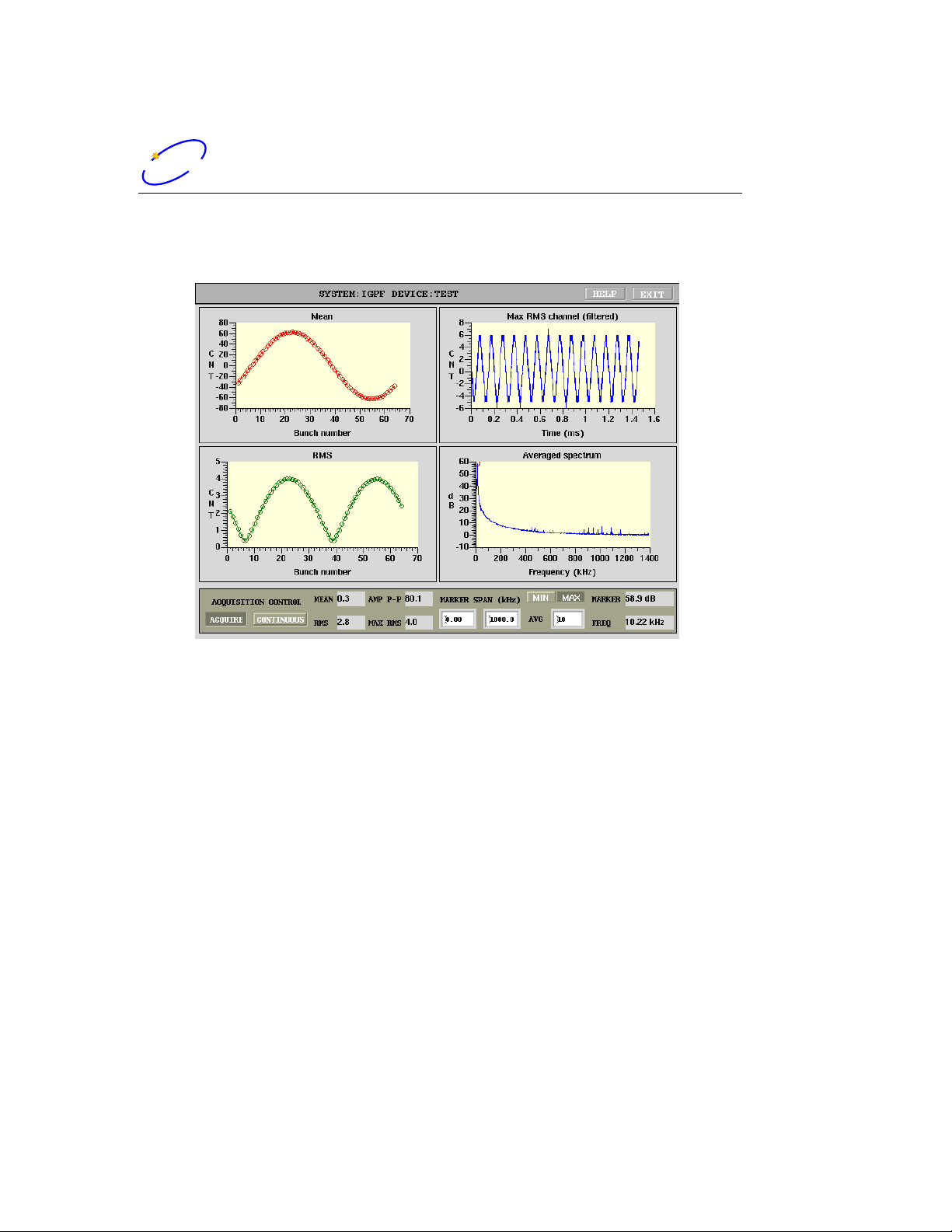
A set of IOC subroutines postprocesses the data in the real-time and provides four concise plots displayed in the waveform panel shown in Figure 11.
The four plots are: bunch-by-bunch mean and root mean square (RMS) of
bunch oscillations, time-domain signal of a bunch with the largest RMS.
The last plot is obtained by performing the fast Fourier transform (FFT) on
each of the bunches and quadratically averaging the resulting spectra. This
plot aliases all coupled-bunch eigenmodes to a frequency span from DC to
ω
/2. Such a spectrum allows the operator to very quickly check how well
rev
the system damps the coupled-bunch motion.
DATA ACQUISITION CONTROL ON/OFF Data acquisition enable.
Turn this control to on to acquire and postprocess the data.
CONTINUOUS/SINGLE Selects between single acquisition mode and
continuous updates.
MEAN Overall mean of the data.
27 of 58
Page 30

5.3 Display Panels
dimtel
dimtel
RMS Overall RMS of the data.
AMP P-P Peak-to-peak amplitude of the gap transient.
MAX RMS Largest RMS around the turn.
MARKER RANGE Lower and upper bounds of a frequency search range
in kHz. Within this frequency range the IOC code searches the averaged spectrum and based on the search type finds maximum (peak) or
minimum (notch) value and frequency.
MIN/MAX Spectrum search type: minimum or maximum. Maximum
search is used for tracking positive peaks, e.g. in driven tune monitoring or in open loop. When the feedback loop is closed a notch typically
forms in the spectrum at the tune frequency. Minimum search can then
be used to provide parasitic non-invasive tune readout.
AVG Spectrum averaging constant. Value roughly corresponds to averaging
time constant expressed in spectrum updates. For example, setting this
field to 10 produces exponential time constant of 10 seconds at 1 Hz
update rate. Value of 1 disables averaging.
MARKER Marker amplitude in dB.
FREQ Marker frequency in kHz.
5.3.8 Environmental Monitoring Panel
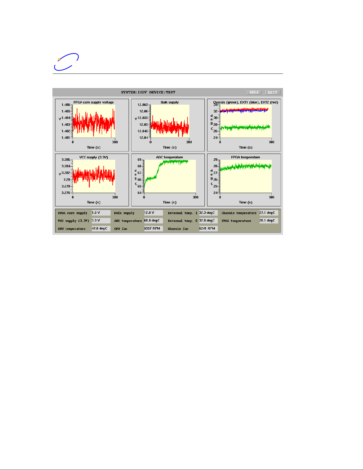
The environmental monitoring panel shown in Figure 12 provides instantaneous readouts and five minute histories of three supply voltages and five
temperatures in the iGp-5120F system. It also monitors IOC CPU temperature and two cooling fan speeds: one mounted on the IOC CPU and the
main chassis fan.
NOTE: The user must check the device temperatures after the unit is installed in the final location to make sure sufficient airflow reaches the internal
devices.
NOTE: Check device temperatures periodically and compare to measurements made during installation. Elevated temperatures can indicate blocked
air intake filter!
28 of 58
Page 31
dimtel
dimtel
5.3 Display Panels
Figure 12: Environmental monitoring panel
The iGp-5120F can continue operating with the main chassis fan stopped,
however such operation puts high stress on certain key semiconductor devices.
Prolonged operation without main chassis fan should be avoided.
5.3.9 Device Controls Panel
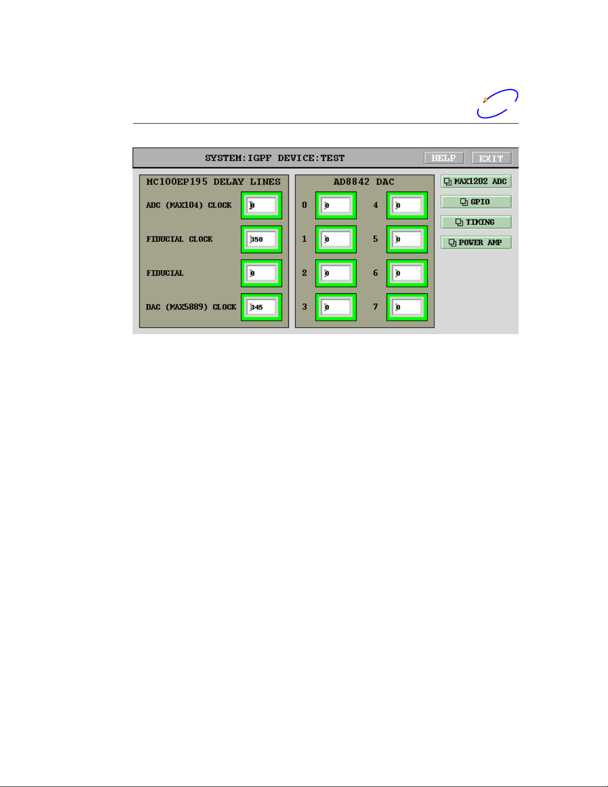
Device controls panel provides control interface to several peripherals integrated in the iGp-5120F. There are four adjustable delay units for controlling
the high-speed ADC, DAC, and fiducial timing.
WARNING: While these delay controls can be used to adjust various clock timings, one is strongly advised to perform the adjustments via the timing panel. Timing panel controls interface to a
sophisticated IOC routine which in turn computes the necessary
settings of the four delay units.
In addition to delay devices this panel provides controls for the low-speed
eight channel DAC. Channels 0 though 6 are brought out on the front-panel
29 of 58
Page 32
5.3 Display Panels
dimtel
dimtel
Figure 13: Device controls panel
connector. Channel 7 is used to trim the output offset of the high-speed DAC.
That setting is preconfigured at the factory and should not be changed.
From the device control panel one can open four other panels: MAX1202
ADC (section 5.3.10), GPIO (section 5.3.11), TIMING (section 5.3.5), and
POWER AMP (section 5.4.
30 of 58
Page 33
dimtel
dimtel
5.3.10 8-channel ADC Panel
Figure 14: 8-channel ADC panel
5.3 Display Panels
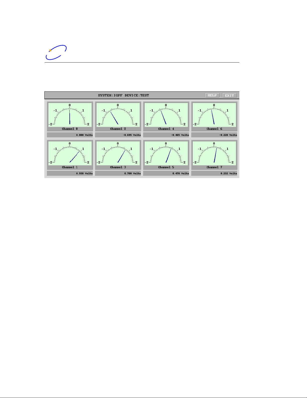
This panel provides readouts of the eight 12-bit ADC channels updated
at 1 Hz. The input signals are low-pass filtered to 1 kHz before sampling.
5.3.11 GPIO Panels
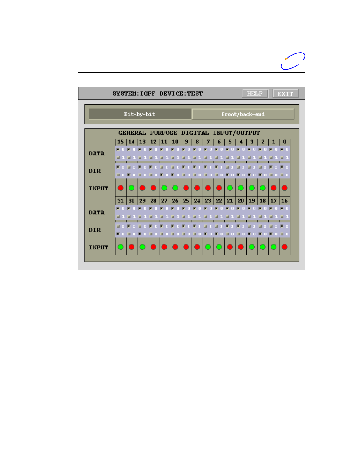
General-purpose I/O control panel in practice consists of two different panels,
one for bit-by-bit GPIO driver and one for the front/back-end driver. Using
the choice buttons on the top of the panel one can select one of the two
drivers.
WARNING: Front/back-end driver sets several I/O pins as outputs. Make sure correct hardware is connected to the GPIO port
before selecting this driver! Improper driver selection may cause
damage to the output pins and the connected external devices.
Bit-by-bit control panel, shown in Figure 15 provides individual bit controls for 32 LVTTL signals available on the rear panel. Each bit control includes output value (0 or 1), direction (In or Out), and the readback. When
the signal is configured for output the readback should reflect the output
value.
31 of 58
Page 34
5.3 Display Panels
dimtel
dimtel
Figure 15: General-purpose I/O panel: bit-by-bit driver
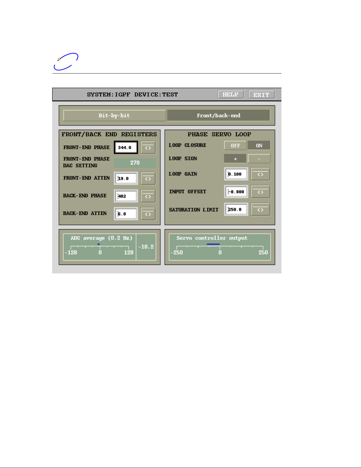
Figure 16 shows the front/back-end panel. This panel is split into two
portions: front/back-end registers and the phase servo loop. The register controls include front and back-end phase and attenuation. Front-end phase register setting is provided as a readout labeled FRONT-END PHASE DAC SETTING. When the phase servo loop is open the register is directly driven by
the front-end phase control setpoint. Closed phase servo loop adjusts the
register value around the setpoint to center the ADC signal. Front and backend attenuation settings adjust digital attenuators in steps of 0.5 dB. Control
values are in dB and are rounded automatically. Full adjustment range is
from 0 to 31.5 dB.
Phase servo loop can be closed and opened by the LOOP CLOSURE
32 of 58
Page 35
dimtel
dimtel
5.3 Display Panels
Figure 16: General-purpose I/O panel: front/back-end driver
buttons. Depending on which zero crossing the phase shifter is centered different loop polarities need to be selected using LOOP SIGN. LOOP GAIN
parameter must be adjusted to optimize the loop response in terms of noise,
bandwidth, and overshoot. Typically the optimization can be c arried out
with beam by stepping the input offset and observing the phase servo response using a stripchart tool. INPUT OFFSET is used to zero out possible
mixer offset or, alternatively, to introduce an offset. Such an offset is typically
used when the beam loading transient is highly asymmetric to avoid reaching
ADC saturation prematurely. SATURATION LIMIT parameter defines the
maximum deviation from the phase setpoint that can be introduced by the
phase servo. This limit must be set below π/2 to make sure the phase servo
33 of 58
Page 36

5.4 Power Amplifier Panel
dimtel
dimtel
does not transition from one zero crossing to another.
Readouts on the bottom provide information on the ADC input offset and
the phase servo output. The bar indicator and the readout on the left show
the output of a Cascaded Integrator Comb (CIC) decimator which averages
109input samples (0.22 Hz −3 dB bandwidth). The indicator on the right
shows the phase servo correction applied to the setpoint. This indication
can be used to adjust the setpoint for near-zero correction. Such near-zero
correction is optimal for closed/open phase servo loop transitions and for low
beam current operation.
5.4 Power Amplifier Panel
iGp-5120F IOC includes driver support for Milmega power amplifier, model
AS0102-200. IOCcan communicate with the amplifier via USB or RS-232
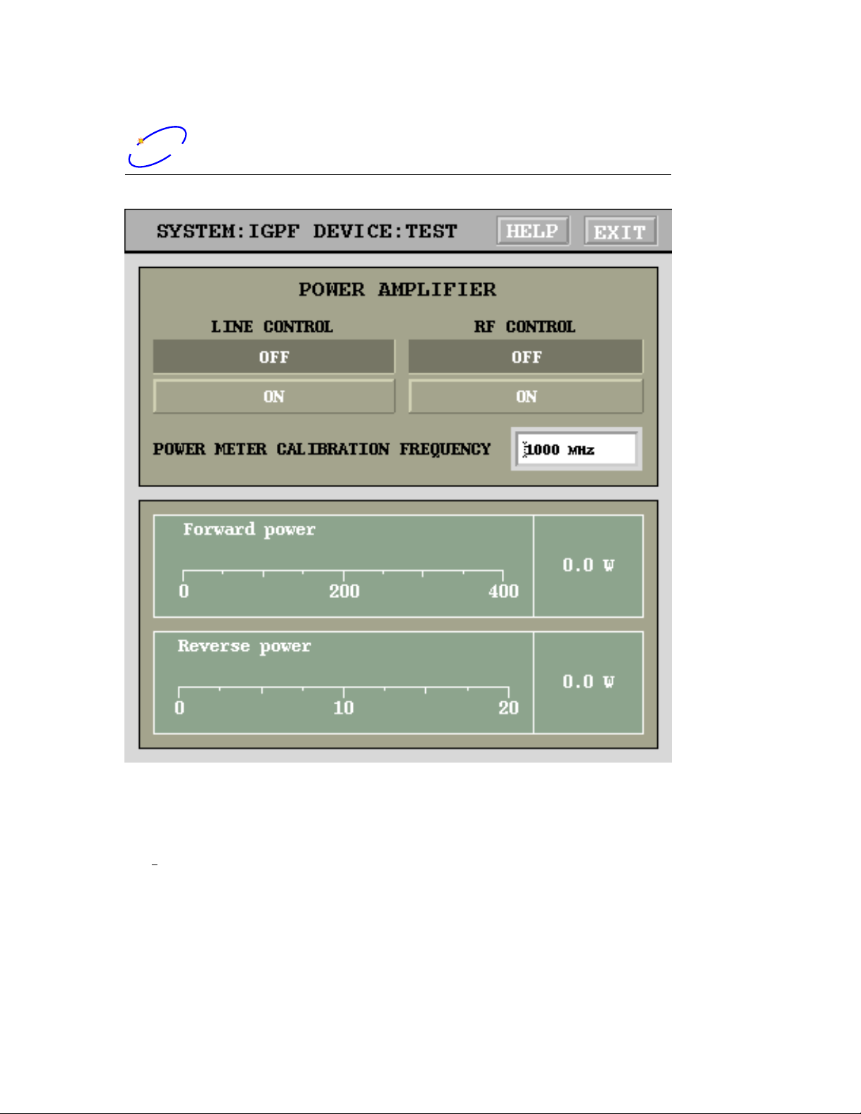
serial port. Control and monitoring functions are combined on the power
amplifier panel shown in Fig. 17. Two control functions are available: line
and RF. Line power switch turns main power supply on and off. That also
controls the state of the cooling fans. RF control enables actual amplifier
operation. Both controls will show inconsistencies between EPICS setting
and amplifier readback in magenta. Two power meter readings are monitored at 1 Hz: forward and reverse power. Internally, Milmega amp lifers
store calibration tables for these power monitors. POWER METER CALIBRATION FREQUENCY setting allows the user to select calibration value
appropriate for the output frequency used.
6 External Software Interface
Software distribution CD includes several tools extract iGp-5120F data for
analysis and processing in external software programs. These tools are written for MATLAB®and use LabCA package for communicating with EPICS.
iGp read Top-level data acquisition tool. This script will read out data
from the iGp-5120F, create a timestamped directory, and save the data
in a file called gd.mat. This file is in a format, compatible with MATLAB®data analysis tools, developed for ALS/LNF-INFN/SLAC longitudinal feedback systems.
34 of 58
Page 37
dimtel
dimtel
External Software Interface
Figure 17: Power amplifier control and monitoring panel
get data This function reads out the raw data vector from the IOC and
returns it to the caller. A single argument is the PV root name, e.g.
IGPF:TEST:.
adctest This function extracts the iGp-5120F data and fits a sinewave to
it. It accepts the IOC device name and the number of times to repeat
the acquisition/fitting cycle.
35 of 58
Page 38

Specifications
dimtel
dimtel
7 Specifications
Table 1: General specifications
Parameter Definition
Operating frequency 509 MHz
RF input level −9 to 3 dBm, -3 dBm nominal
Number of FIR taps 8
Harmonic number 5120
Fiducial signal Falling edge trigger, NIM level
Minimum fiducial pulse width 1.96 ns
External trigger inputs 2 inputs, NIM level, falling edge
Minimum trigger pulse width 3.93 ns
Data acquisition memory
(SRAM)
FPGA dual-port memory
(blockRAM)
Slow analog inputs 8 channels @12 bits, -2.048 to 2.048 V
Slow analog outputs 7 channels @8 bits, −1 to 1 V swing
General purpose digital I/O 32 bits in/out, LVTTL
8 Msamples
128 ksamples
into 50 Ω
36 of 58
Page 39

dimtel
dimtel
Specifications
Table 2: High-speed ADC and DAC specifications
Parameter Definition
ADC inputs 2 complementary
ADC input full scale sensitivity 200 mV peak-to-peak (−10 dBm)
ADC resolution 8 bits
ADC input bandwidth 1.26 GHz
DAC outputs 2 complementary
DAC FS 500 mV peak-to-p eak (−2 dBm)
DAC resolution 12 bits
DAC rise time (10%-90% FS) under 250 ps
DAC fall time (90%-10% FS) under 350 ps
Table 3: FIR filter control
Parameter Definition
Coefficients 16 bit wide in Q15 format
Coefficient sets 2
Coefficient set select 0 or 1
FIR channel enable control On/Off
Shift gain 0 to 7
Downsampling 1 to 32
Table 4: Control parameters
Parameter Definition
One-turn delay adjustment TRFper step, up to one revolution
DCM reset Control panel pushbutton
DCM phase −180 to 180 degrees in 256 steps
Clock and fiducial delays 4 channels
Clock and fiducial delay step 10 ps
Clock and fiducial delay range 0–10.23 ns
General-purpose analog outputs 7 channels
High-speed DAC offset adjustment
General-purpose digital outputs 32 inputs/outputs
1 channel
37 of 58
Page 40

Specifications
dimtel
dimtel
Table 5: Data acquisition controls
Parameter Definition
Recording memory selection FPGA internal blockRAM or external
SRAM
Measurement trigger Internal or external
External trigger arming Single or after every beam data read-
out
Recorded growth length Adjustable in units of 4 samples, up to
full memory length
Hold-off before recording In units of 4 samples, 0 to 232− 1
Recording downsampling 1 to 32
Table 6: Monitoring and diagnostics
Parameter Definition
Clock status RF clock missing, DCM lock
Feedback channel status FIR saturation
Acquisition state machine status Trigger arming bit
Voltages FPGA core supply, 3.3 V, 12 V bulk
Temperatures Fast ADC, FPGA, ambient, two
emitter coupled logic (ECL) devices,
IOC CPU
Fan speeds Chassis and CPU IOC
Analog inputs 8 slow ADC channels
Digital inputs 32 general-purpose inputs/outputs
38 of 58
Page 41

dimtel
dimtel
Specifications
Table 7: Drive patte rn generator
Parameter Definition
Output waveform Sine, sawtooth, square, or arbitrary
Amplitude 0–1
Bunch selectability Bunch-by-bunch drive enable mask.
Allows any subset of bunches to be
driven
Frequency range, bunch-by-bunch
mode
Frequency range, turn-by-turn
mode
0–Frf/2
0–F
rev
/2
Table 8: Input Power Requirements
Parameter Definition
Input voltage 115/230 VAC
Input current 2/1 A
Frequency 60/50 Hz
Voltage selection Switch
Low voltage range 104–126 V
High voltage range 207–253 V
39 of 58
Page 42

Warranty and Support
dimtel
dimtel
8 Warranty and Support
8.1 Warranty
Dimtel Inc. warranties this product for a period of one year from the date
of shipment against defective workmanship or materials. This warranty excludes any defects, failures or damage caused by improper use or inadequate
maintenance, installation or repair performed by Customer or a third party
not authorized by Dimtel, Inc. Warrantied goods will be either repaired or
replaced at the discretion of Dimtel, Inc. The above warranties are exclusive
and no other warranty, whether written or oral, is expressed or implied.
8.2 Support
Dimtel Inc. will provide technical support for the product free of charge for
a period of one year from the date of shipment. Such support is defined to
include:
FPGA gateware bug fixes and upgrades;
IOC software bug fixes and upgrades;
Client software (display panels, external interface) bug fixes and upgrades;
Phone, e-mail, and remote access (when allowed by the Customer)
support of software and hardware integration.
Free of charge technical support specifically excludes:
Commissioning with beam;
Feedback algorithm development and testing;
Beam dynamics characterization;
Operational support related to dynamic system operation.
40 of 58
Page 43

dimtel
dimtel
Appendix A: Address Map
9 Appendix A: Address Map
9.1 Registers
9.1.1 Overall Layout
The general register layout for the iGp-5120F reserves space below 0x100 for
FIR coefficients. This allows for a maximum of 128 coefficients in two sets.
Control and status registers are placed starting at 0x100.
Table 9: FPGA registers: FIR
Address Bits Definition
0x000000 15:0 FIR coefficient 0, set 0
0x000001 15:0 FIR coefficient 0, set 1
0x000002 15:0 FIR coefficient 1, set 0
0x000003 15:0 FIR coefficient 1, set 1
0x000004 15:0 FIR coefficient 2, set 0
0x000005 15:0 FIR coefficient 2, set 1
0x000006 15:0 FIR coefficient 3, set 0
0x000007 15:0 FIR coefficient 3, set 1
0x000008 15:0 FIR coefficient 4, set 0
0x000009 15:0 FIR coefficient 4, set 1
0x00000a 15:0 FIR coefficient 5, set 0
0x00000b 15:0 FIR coefficient 5, set 1
0x00000c 15:0 FIR coefficient 6, set 0
0x00000d 15:0 FIR coefficient 6, set 1
0x00000e 15:0 FIR coefficient 7, set 0
0x00000f 15:0 FIR coefficient 7, set 1
0x000010 15:0 FIR coefficient 8, set 0
0x000011 15:0 FIR coefficient 8, set 1
0x000012 15:0 FIR coefficient 9, set 0
0x000013 15:0 FIR coefficient 9, set 1
0x000014 15:0 FIR coefficient 10, set 0
0x000015 15:0 FIR coefficient 10, set 1
0x000016 15:0 FIR coefficient 11, set 0
0x000017 15:0 FIR coefficient 11, set 1
Continued on next page
41 of 58
Page 44

9.1 Registers
dimtel
dimtel
Table 9 – continued from previous page
Address Bits Definition
0x000018 15:0 FIR coefficient 12, set 0
0x000019 15:0 FIR coefficient 12, set 1
0x00001a 15:0 FIR coefficient 13, set 0
0x00001b 15:0 FIR coefficient 13, set 1
0x00001c 15:0 FIR coefficient 14, set 0
0x00001d 15:0 FIR coefficient 14, set 1
0x00001e 15:0 FIR coefficient 15, set 0
0x00001f 15:0 FIR coefficient 15, set 1
9.1.2 Gateware Config Register
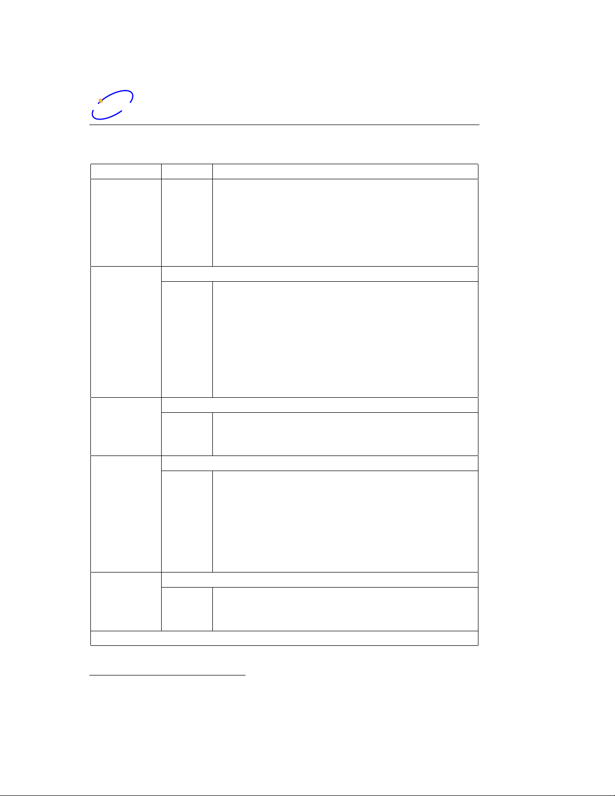
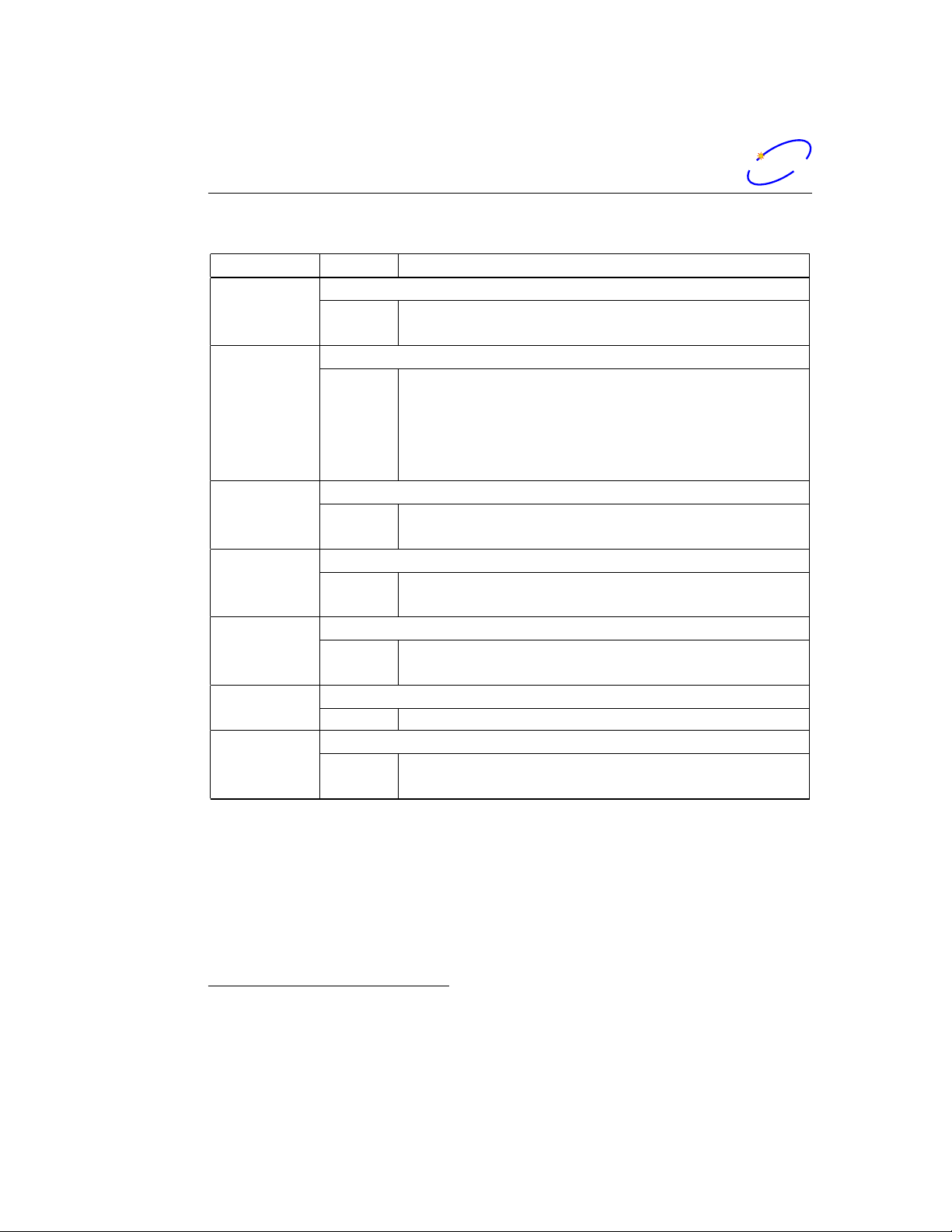
Gateware config register (0x107) provides information about the unit’s functionality, gateware revision, harmonic number, and processing demultiplexing.
Table 10: FPGA registers: control and status
Address Bits Definition
Main control register
0 Data acquisition trigger
1 Reserved
2 Coefficient set select, 0 - set 0, 1 - set 1
0x000100
3 FIR channel disable, 1 - disabled
6:4 Shift gain, 0 through 7
7 DCM reset
8 Grow/damp enable
9 Trigger select, 1 - external
10 External trigger arming, arms on rising edge
11 SRAM interface select, 0 - local bus, 1 - ADC
12 ADC test pattern generator enable
1
Gateware revision 1.2 and higher
42 of 58
1
Continued on next page
Page 45
dimtel
dimtel
Table 10 – continued from previous page
Address Bits Definition
13 DAC drive phase: 0 - 0 degrees, 1 - 180 degrees
14 Turn-by-turn mode of the arbitrary waveform gen-
erator
2
15 Arbitrary waveform generator enable
16 GPIO driver select, 0 - bit-by-bit, 1 - FBE
31-17 Reserved
Status register, reset on read
0 RF clock missing
0x000101
1 Saturation
2 Processing DCM unlocked
3 External trigger arming status
4 Local bus clo ck DCM unlocked
5 Fiducial error
6 Acquisition DCM unlocked
31:7 Reserved
DCM phase shift register
0x000102
8:0 Phase shift, default 0x100 (0 deg), range
0x80(−π) to 0x180 (π)
31:9 Unused, read out as 0
Output delay length
0x000104
9:0 Delay length in units of 4 samples
10 Reserved
15:11 Recording downsampling, 0 - every turn, Nds=
regval + 1
20:16 Processing downsampling
26:24 Fine delay adjustment, one sample per step
31:27 Reserved
0x000105
20:0 Number of samples to hold setsel inverted during
Grow/damp filter 2 length
data acquisition (growth length)
31:21 Reserved
Continued on next page
9.1 Registers
2
2
3
2
Gateware revision 1.3 and higher
3
Gateware revision 1.4 and higher
43 of 58
Page 46
9.2 Drive pattern memory
dimtel
dimtel
Table 10 – continued from previous page
Address Bits Definition
0x000106
31:0 Number of samples to hold setsel inverted before
Hold-off length
data acquisition
0x000107
12:0 Harmonic number
Gateware config register (read-only)
14:13 Demux mode, 0 - by4, 1 - by6, 2 - by8, 3 - reserved
15 Reserved
23:16 Gateware revision
31:24 Gateware functionality, 0 - feedback
0x000108
11:0 Fiducial delay, two samples per step
Fiducial delay
31:12 Reserved
0x000109
20:0 Acquisition length in units of 4 samples
Acquisition length
31:21 Reserved
0x000200
0 Acquisition in progress, memory busy
Acquisition status (read-only)
31:2 Reserved
0x000201
0x000202
31:0 Test pattern start value
31:0 Decimated input average, direct current (DC)
gain of 15.625 × 10
ADC test counter start
CIC mean output (read-only)
6
4
5
9.2 Drive pattern memory
An arbitrary waveform generator with bunch-by-bunch masking is integrated
in the FPGA gateware. The generator uses two memory blocks to define the
waveform and the bunch mask as documented in Table 11.
4
Gateware revision 1.2 and higher
5
Gateware revision 1.4 and higher
44 of 58
Page 47
dimtel
dimtel
9.3 Environmental monitor
Table 11: Drive patt er n memory
Address Bits Definition
0x040000-0x45fff 8:0 Drive pattern memory, even samples
0x040000-0x45fff 20:12 Drive pattern memory, odd samples
0x048000-0x487ff 3:0 Bunch mask memory, bit 0 - first
bunch, bit 1 - last
9.3 Environmental monitor
iGp-5120F uses two MAX1299 devices for monitoring five temperatures and
three power supply voltages. The SPI interface module for the controller
uses sixteen addresses, as described in table 12.
Let’s consider the first device (addresses 0x110–0x117). Analog inputs 0
and 1 (AIN0, AIN1) are connected to the FPGA temperature diode. General
conversion function from the raw register value to temperature in degrees
Celsius is x/32 − 273.15. Analog inputs 2 and 3 are used to measure the
temperature of the MAX104 ADC. The ADC provides two current sources
I
and I
ptat
300I
ptat/Ipconst
resistors and connected to AIN2 and AIN3.
MAX1299 also measures the ambient chassis temperature via the internal
diode. Two supply voltages are measured: FPGA core (1.5 V) connected to
AIN4 and 3.3 V supply internally measured by MAX1299. Raw register value
can be converted to voltage by 2.4×X/16384. For the 3.3 V supply the value
must be multiplied by 4, since MAX1299 monitors Vdd/4.
The second device is configured for external temperature sensors at AIN0–
AIN1 and AIN2–AIN3. AIN4 is connected to a resistive divider monitoring
bulk 12 V supply. Divider ratio is 1/6 for 2 V nominal ADC input.
for temperature measurement. ADC temperature is given by
pconst
− 273. In the iGp-5120F the two sources are loaded by 5.1 kΩ
Table 12: FPGA registers: MAX1299 monitors
Address Bits Definition
0x000110 15:0 Device 1, AIN2 (V
0x000111 15:0 Device 1, AIN3 (V
)
ptat
pconst
)
0x000112 15:0 Device 1, AIN4, FPGA core voltage V
Continued on next page
int
45 of 58
Page 48
9.4 MAX1202 8-channel ADC
dimtel
dimtel
Table 12 – continued from previous page
Address Bits Definition
0x000113 15:0 Device 1, Internal diode
0x000114 15:0 Device 1, Vdd/4, 3.3 V supply monitor
0x000115 15:0 Device 1, External diode (AIN0/AIN1), FPGA
die temperature
0x000116 15:0 Device 1, AIN2-AIN3 differential measurement
0x000117 15:0 Device 1, AIN5-AIN5 differential measurement
0x000118 15:0 Device 2, AIN2
0x000119 15:0 Device 2, AIN3
0x00011a 15:0 Device 2, AIN4, bulk supply monitor
0x00011b 15:0 Device 2, Internal diode
0x00011c 15:0 Device 2, Vdd/4, 3.3 V supply monitor
0x00011d 15:0 Device 2, External diode (AIN0/AIN1)
0x00011e 15:0 Device 2, External diode (AIN2/AIN3)
0x00011f 15:0 Device 2, AIN5-AIN5 differential measurement
9.4 MAX1202 8-channel ADC
iGp-5120F includes 8-channel 12-bit serial-interface ADC. The SPI controller
for the ADC uses 8 consecutive addresses, as shown in Table 13. ADC is
continuously polled by the controller. Reading one of the channel registers
returns the result of the last conversion. ADC data is sign extended from 12
bits to 16. The valid data range is from 0xf800 to 0x7ff. ADC input range
is from −2.048 to 2.047 V, i.e. 1 mV per LSB.
Table 13: FPGA registers: MAX1202 ADC
Address Bits Definition
0x000120 11:0 ADC channel 0
0x000121 11:0 ADC channel 1
0x000122 11:0 ADC channel 2
0x000123 11:0 ADC channel 3
0x000124 11:0 ADC channel 4
Continued on next page
46 of 58
Page 49
dimtel
dimtel
9.5 AD8842 8-channel DAC
Table 13 – continued from previous page
Address Bits Definition
0x000125 11:0 ADC channel 5
0x000126 11:0 ADC channel 6
0x000127 11:0 ADC channel 7
9.5 AD8842 8-channel DAC
iGp-5120F includes 8-channel 8-bit serial-interface DAC. The SPI controller
for the DAC uses 8 consecutive addresses, as shown in Table 14. Writing to
one of the registers starts an SPI writing cycle which loads the new value
into the DAC. On writes only the 8 LSB are used. Register reads are signextended to 16 bits. DAC reference voltage is 3 V for −3 to +3 V output
range. Output drivers generate full swing into high-impedance loads. For
50 Ω loads the swing is reduced to 1 V.
Unlike other DAC channels, channel 7 is not brought out to the frontpanel connector. Its output is used to trim the DC level of the high-speed
DAC. The output is attenuated to produce ±5 % of full-scale adjustment of
the DC level.
Table 14: FPGA registers: AD8842 DAC
Address Bits Definition
0x000128 7:0 DAC channel 0
0x000129 7:0 DAC channel 1
0x00012a 7:0 DAC channel 2
0x00012b 7:0 DAC channel 3
0x00012c 7:0 DAC channel 4
0x00012d 7:0 DAC channel 5
0x00012e 7:0 DAC channel 6
0x00012f 7:0 DAC channel 7
47 of 58
Page 50
9.7 General-purpose digital I/O
dimtel
dimtel
9.6 ECL delay lines
Several MC100EP195 ECL delay lines are use d on the iGp-5120F to line up
the received RF clock and the fiducial signal. These lines are controlled by
registers described in Table 15.
Delay line 0 controls the delay of the ADC clock. Relative delay between
lines 1 and 2 is used to achieve reliable detection of the fiducial falling edge
in the front-end. Once that relative delay is determined, both 1 and 2 must
be adjusted together to achieve proper timing between the fiducial (reset)
pulse to the ADC and the ADC clock. This second stage fixes relative delays
between 0, 1, and 2. Finally, delay line 3 must be adjusted to achieve optimal
placement of the DAC clock relative to the FPGA data.
Table 15: FPGA registers: ECL delay lines
Address Bits Definition
0x000130 9:0 Delay line 0 (ADC clock)
0x000131 9:0 Delay line 1 (Fiducial clock)
0x000132 9:0 Delay line 2 (Fiducial)
0x000133 9:0 Delay line 3 (DAC clock)
9.7 General-purpose digital I/O
There are two distinctly different drivers implemented in the gateware for the
control of the general-purpose digital I/O port of the iGp-5120F. A generic
bit-by-bit driver is accessed when bit 16 of the main control register (0x100)
is set to 0. The port is accessed via three registers listed in Table 16.
Table 16: FPGA registers: bit-by-bit GPIO
Address Bits Definition
0x000138 31:0 Output data
0x000139 31:0 Direction (1 - out, 0 - in)
0x00013a 31:0 Pin value readback
48 of 58
Page 51
dimtel
dimtel
9.8 Memory
A custom driver designed for interfacing to Dimtel, Inc. longitudinal
front/back-end units (FBE) is selected when bit 16 of the main control register is set to 1. The custom driver is included in the gateware starting from
version 1.4. Front and back-end phase settings control carrier phases in the
front and the back-end respectively. Offset-binary DAC setting in each case
provides adjustment range of ≈ 400 degrees at the carrier frequency. Front
and back-end attenuation settings are in 0.5 dB steps for a total range of
31.5 dB.
Table 17: FPGA registers: Front/back-end GPIO
Address Bits Definition
0x00013c 11:0 Front-end phase
0x00013d 11:0 Back-end phase
0x00013e 5:0 Front-end attenuation
0x00013f 5:0 Back-end attenuation
9.8 Memory
iGp-5120F is configured with two data acquisition memory spaces: blockRAM internal to the FPGA and external SRAM. Memory address mapping
is provided in Table 18.
Table 18: Data acquisition memory
Address range Definition
0x010000-0x017fff 32k×32 blo ckRAM (128 ksamples)
0x800000-0xa00000 2M×32 SRAM (8 Msamples)
49 of 58
Page 52
Appendix B: Connector Pinouts
dimtel
dimtel
1416 12 10 8 6 4 2
13579111315
10 Appendix B: Connector Pinouts
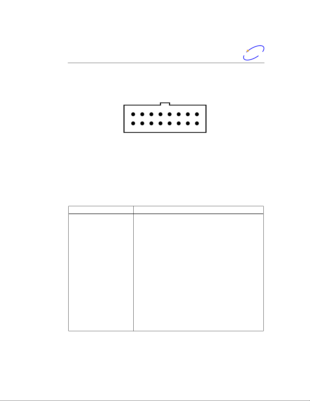
Figure 18: Pin numbering for 16-pin header-type front-panel connectors
Pin numbering scheme for the 16-pin front-panel connectors is shown in
Figure 18. Pin definitions for the 7-channel DAC are given in Table 19 and
for the 8-channel DAC - in Table 20.
Table 19: 7-channel DAC pinout
Pin number Definition
1 Channel 0
2 GND
3 Channel 1
4 GND
5 Channel 2
6 GND
7 Channel 3
8 GND
9 Channel 4
10 GND
11 Channel 5
12 GND
13 Channel 6
14 GND
15 N/C
16 GND
50 of 58
Page 53
dimtel
dimtel
Appendix B: Connector Pinouts
686766656463626160595857565554535251504948474645444342414039383735 36
3433323130292827262524232221201918171615141312111098765431 2
Table 20: 8-channel ADC pinout
Pin number Definition
1 Channel 7
2 GND
3 Channel 6
4 GND
5 Channel 5
6 GND
7 Channel 4
8 GND
9 Channel 3
10 GND
11 Channel 2
12 GND
13 Channel 1
14 GND
15 Channel 0
16 GND
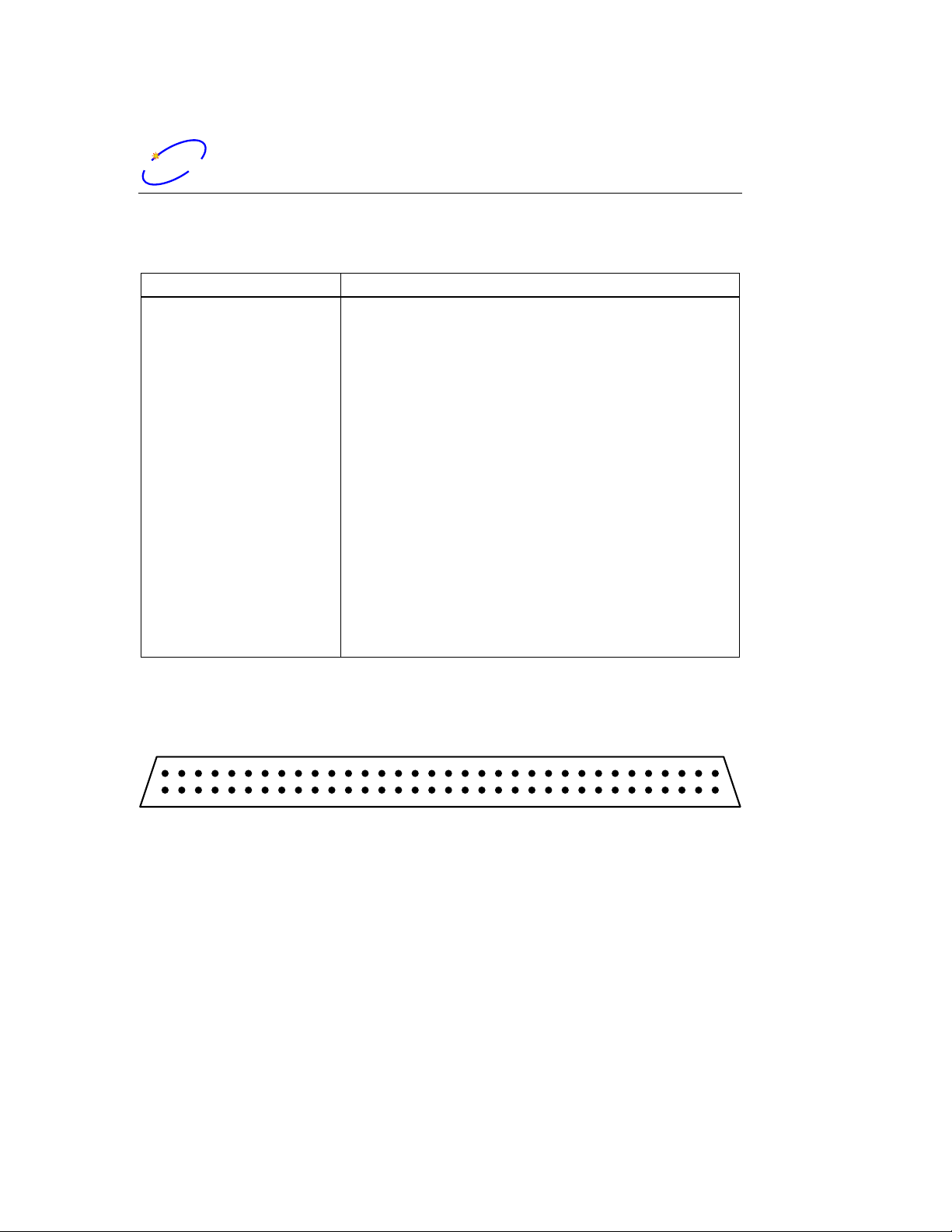
Figure 19: Pin numbering for general-purpose digital I/O connector
Figure 19 shows the pin numbering for the general-purpose digital I/O
connector. Pin definitions are listed in Table 21.
51 of 58
Page 54

Appendix B: Connector Pinouts
dimtel
dimtel
Table 21: General-purpose digital I/O pinout
Pin number Definition
1 Bit 31
2 Bit 30
3 Bit 29
4 Bit 28
5 Bit 27
6 Bit 26
7 Bit 25
8 Bit 24
9 Bit 23
10 Bit 22
11 Bit 21
12 Bit 20
13 Bit 19
14 Bit 18
15 Bit 17
16 Bit 16
17 GND
18 Bit 15
19 Bit 14
20 Bit 13
21 Bit 12
22 Bit 11
23 Bit 10
24 Bit 9
25 Bit 8
26 Bit 7
27 Bit 6
28 Bit 5
29 Bit 4
30 Bit 3
31 Bit 2
32 Bit 1
33 Bit 0
Continued on next page
52 of 58
Page 55

dimtel
dimtel
Appendix B: Connector Pinouts
Table 21 – continued from previous page
Pin number Definition
34 Bit N/C
35 GND
36 GND
37 GND
38 GND
39 GND
40 GND
41 GND
42 GND
43 GND
44 GND
45 GND
46 GND
47 GND
48 GND
49 GND
50 GND
51 GND
52 GND
53 GND
54 GND
55 GND
56 GND
57 GND
58 GND
59 GND
60 GND
61 GND
62 GND
63 GND
64 GND
65 GND
66 GND
67 GND
68 N/C
53 of 58
Page 56

Appendix B: Connector Pinouts
dimtel
dimtel
54 of 58
Page 57

dimtel
dimtel
11 Glossary
Glossary
analog-to-digital converter (ADC)
An electronic circuit that converts continuous analog signals to discrete
digital numbers. 5, 6, 9, 13, 15, 23, 24, 29, 31, 32, 34, 36, 42, 43, 45,
46, 48
blockRAM
Random access memory integrated in Xilinx®FPGA in a form of multiple 18 kbit blocks. 15, 19, 36, 49
Cascaded Integrator Comb (CIC)
A discrete-time filter, which efficiently averages a large number of input samples. Such filters are typically used for sampling rate changes
(decimation and interpolation). 34, 43
Glossary
digital-to-analog converter (DAC)
A hardware device to convert a sequence of digital codes to corresponding analog voltages or currents. 4–7, 9, 13, 15, 17, 23–25, 29, 36, 42,
47, 48, 50, 56
direct current (DC)
In electrical engineering context — a constant signal, either voltage or
current. 43
digital clock manager (DCM)
A delay-locked loop (DLL) based clock management circuit integrated
in the Xilinx®FPGA. The circuit allows fine phase adjustment of the
output clock relative to the input. 7, 15, 20, 23, 36, 42
delay-locked loop (DLL)
A device for managing clock skew in digital circuits. 55
55 of 58
Page 58

Glossary
dimtel
dimtel
emitter coupled logic (ECL)
A logic device family in which current is steered through bipolar transistors to compute logical functions. The chief characteristic of ECL is
that the transistors are always in the active region and can thus change
state very rapidly, allowing ECL circuits to op erate at very high speed.
36, 47, 48
extensible display manager (EDM)
A tool that manages a collection of active displays with the ability to
create and edit display content as well as the ability to execute the
same content resulting in the dynamic presentation of live data. 15–17
experimental physics and industrial control system (EPICS)
A set of software tools and applications used to develop distributed soft
real-time control systems. 6, 10, 12, 15, 16, 21, 34, 57
Ethernet
A family of frame-based computer networking technologies for local
area networks. 5, 9
fast Fourier transform (FFT)
An efficient algorithm to compute the discrete Fourier transform. 27
finite impulse response (FIR)
A discrete-time filter, output of which only depends on a finite number
of previous input samples. 4, 6, 17, 19, 20, 36, 41, 42
field programmable gate array (FPGA)
A semiconductor device containing programmable logic components
and programmable interconnects. 5, 6, 12, 13, 15, 19, 24, 36, 41, 42,
44–49
full-scale (FS)
Difference between maximum and minimum limits of the signal. For
example, DAC full-scale is the difference of the outputs for maximum
and minimum codes. 6, 9, 36
56 of 58
Page 59

dimtel
dimtel
input/output (I/O)
An interface for transferring analog or digital signals to or from the
device. 5, 13, 15, 31, 48, 51
input-output controller (IOC)
An embedded computer used to interface the hardware to the control
system. 5, 9–13, 15, 16, 19, 27, 28, 34, 35
Linux
A Unix-like open-source operating system. 5
low-voltage transistor-transistor logic (LVTTL)
Transistor-transistor logic with the same logic thresholds as transistortransistor logic (TTL). LVTTL outputs can be connected directly to
TTL inputs. TTL outputs can drive LVTTL inputs only if the latter
are 5 V tolerant. 8, 31, 36
Glossary
NIM
NIM (originally an acronym for Nuclear Instrumentation Methods)
logic defines signal levels (with 50 Ω termination) of 0 V and −0.8 V
for logic 0 and 1 respectively. 6, 9, 19, 36
process variable (PV)
An individual control or readout signal in EPICS 12, 26, 34
radio frequency (RF)
In the accelerator context, a constant frequency constant amplitude
signal derived from or phase locked to the storage ring master oscillator.
5–7, 9, 13, 20, 23–25, 34, 36, 42
root mean square (RMS)
A statistical measure of the magnitude of a varying quantity. 27, 28
static random access memory (SRAM)
A type of semiconductor memory that retains its contents as long as
the power is applied. 5, 15, 19, 36, 42, 49
57 of 58
Page 60

Glossary
dimtel
dimtel
transistor-transistor lo gi c (TTL)
A class of digital circuits built from bipolar junction transistors and
resistors. TTL defining signal levels: VOH= 2.4 V , VOL= 0.4 V ,
VIH= 2 V, and VIL= 0.8 V 57
universal serial bus (USB)
A serial bus standard to interface a wide variety of devices. 5, 34
58 of 58
 Loading...