

Page 1

ConnectCore® 6UL
System-on-module solution
Hardware Reference Manual
Page 2

Revision history—90001523
Revision Date Description
K October
2019
L April 2020 Updated mechanical drawings to show additional dimensions, updated
M May 2020 Added operating temperature statement, replaced power-up time
N September
2020
P February
2021
Updated LGA_L3 description.
name of Digi Microcontroller Assist, and replaced block diagram.
diagram, modified maximum current power supply note.
Clarified I2C1 support and external supply usage.
Removed variants list and replaced with link to product page.
Trademarks and copyright
Digi, Digi International, and the Digi logo are trademarks or registered trademarks in the United
States and other countries worldwide. All other trademarks mentioned in this document are the
property of their respective owners.
© 2021 Digi International Inc. All rights reserved.
Disclaimers
Information in this document is subject to change without notice and does not represent a
commitment on the part of Digi International. Digi provides this document “as is,” without warranty of
any kind, expressed or implied, including, but not limited to, the implied warranties of fitness or
merchantability for a particular purpose. Digi may make improvements and/or changes in this manual
or in the product(s) and/or the program(s) described in this manual at any time.
Warranty
To view product warranty information, go to the following website:
www.digi.com/howtobuy/terms
Customer support
Gather support information: Before contacting Digi technical support for help, gather the following
information:
Product name and model
Product serial number (s)
ConnectCore® 6UL Hardware Reference Manual
2
Page 3

Firmware version
Operating system/browser (if applicable)
Logs (from time of reported issue)
Trace (if possible)
Description of issue
Steps to reproduce
Contact Digi technical support: Digi offers multiple technical support plans and service packages.
Contact us at +1 952.912.3444 or visit us at www.digi.com/support.
Feedback
To provide feedback on this document, email your comments to
Include the document title and part number (ConnectCore® 6UL Hardware Reference Manual,
90001523 N) in the subject line of your email.
techcomm@digi.com
ConnectCore® 6UL Hardware Reference Manual
3
Page 4

Contents
About the ConnectCore® 6UL
Features and functionality 6
Variants 7
Block diagrams 7
ConnectCore 6UL module 8
NXP i.MX6UL application processor 9
Power interfaces 10
Power supply architecture 10
System power-up sequence 14
Coin cell 15
Bootstrap 16
Boot from fuses 17
Internal boot 18
Serial downloader 19
Wireless interfaces 19
WLAN IEEE 802.11a/b/g/n/ac 19
Antenna ports 24
Bluetooth 25
RF control signals 25
Parallel display 25
Microcontroller Assist™ 26
ConnectCore 6UL module lines related to the MCA 27
Reset control 28
IOs 29
Watchdog 31
Real-time clock 32
Tamper support 32
Power management 33
MCA firmware update 36
CryptoAuthentication device 36
Module pinout - general layout 36
External signals and pin multiplexing 38
Module specifications
Electrical specifications 108
Absolute maximum ratings 108
With front-end LDO 108
Without front-end LDO 108
Undervoltage detection 108
ConnectCore® 6UL Hardware Reference Manual
4
Page 5

Overvoltage detection 109
Power consumption 109
Power consumption use cases 109
Global power consumption 112
Power consumption: Wireless power consumption increase 112
Power consumption: Real wireless transmission 113
Power consumption: Wireless-UART bridge 114
Mechanical specifications 115
Dimensions 115
Host PCB footprint and cutout 116
Weight 118
Environmental specifications 118
Socket options 119
Assembly instructions
Moisture sensitivity and shelf life 121
Mounting 121
Coplanarity 121
Solder paste print 121
Stencil 122
SMT pick and place 122
SMT process parameter reference - castellation and LGA applications 122
Reflow oven profile 122
Vapor phase profile 124
Vapor Phase IBL 309 batch soldering machine settings 125
Conformal coating 125
Regulatory information and certifications
Maximum power and frequency specifications 127
External antenna 127
Bluetooth certification 127
United States FCC 127
FCC notices 128
FCC-approved antennas 128
RF exposure 129
Europe 129
CE mark 129
OEM labeling requirements 130
CE labeling requirements 130
Declarations of Conformity 130
Approved antennas 130
Canada (IC) 130
Labeling requirements 131
Transmitters with detachable antennas 131
RF exposure 131
Approved antennas 132
Japan 132
Approval Label (MIC Marking) 133
ConnectCore® 6UL Hardware Reference Manual
5
Page 6

About the ConnectCore® 6UL
The ConnectCore 6UL is a secure and extremely cost-effective connected System-on-Module platform.
Its innovative Digi SMTplus® surface mount form factor allows you to choose simplified design
integration leveraging proven and easy-to-use edge-castellated SMT technology, or a versatile LGA
option for ultimate design flexibility with access to virtually all interfaces.
Built on the NXP i.MX6UL application processor, the module is the intelligent communication engine
for today’s secure connected devices. It integrates dual-Ethernet and pre-certified dual-band Wi-Fi
(802.11a/b/g/n/ac) with dual mode Bluetooth 4.2 connectivity.
Features and functionality
The ConnectCore 6UL system-on-module is based on the i.MX6UL processor from NXP. This processor
offers a number of interfaces, most of them multiplexed and not available simultaneously. The module
has the following features:
l i.MX6UL single ARMCortex-A7 core operating at speeds up to 528 MHz:
o
32 Kb L1 instruction cache
o
32 Kb L1 data cache
o
Up to 128 KB unified instruction/data L2 cache
o
NEONMPE (media processing engine) co-processor
l Up to 1 GB, 16-bit DDR3-800 memory
l Up to 2 GB, 8-bit SLC NAND flash memory
l NXP PF3000 power management IC (PMIC):
o
x 4 DC/DC buck converters
o
x 6 LDO regulators
o
x 1 DC/DC boost converter
o
OTP (one-time programmable) memory
o
Coin cell charger and always-ON RTC supply
l Graphical hardware accelerators:
o
PXP (PiXel Processing Pipeline)
o
ASRC (asynchronous sample rate converter)
l Secure Element
l Security accelerators:
ConnectCore® 6UL Hardware Reference Manual
6
Page 7

About the ConnectCore® 6UL Variants
o
ARMTrustZone
o
CAAM (cryptographic acceleration and assurance module)
o
SNVS (secure non-volatile storage)
o
CSU (central security unit)
o
A-HABv4 (advanced high-assurance boot)
l IEEE 802.11 a/b/g/n/ac WLAN interface
l Bluetooth®version 4.2 dual-mode
l ARM Cortex-M0+ Microcontroller Assist™ (MCA) subsystem
l Debug interfaces:
o
System JTAG controller
o
Single Wired Debug (SWD) interface for the MCA
l Support of i.MX6UL interfaces:
o
16-bit data/address bus
o
Display: 24-bit parallel bus
o
Camera: 24-bit parallel bus
o
KPP (key pad port)
o
TSC (touch screen controller)
o
x 2 MMC/SD/SDIO card ports
o
x 2 USB 2.0 OTG with integrated HS USB PHYs
o
x 2 10/100 Mbps Ethernet MAC
o
UART, SPI, I2C, PWM, ADC, CAN, I2S, and GPIOs
l Ultra-miniature SMT module (29 x 29 x 3.5 mm) based on 245 pads (245 LGA, 76 also available as
castellated pads)
Variants
See the ConnectCore 6UL product page for information on available variants.
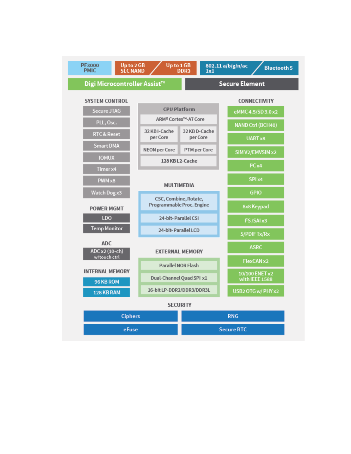
Block diagrams
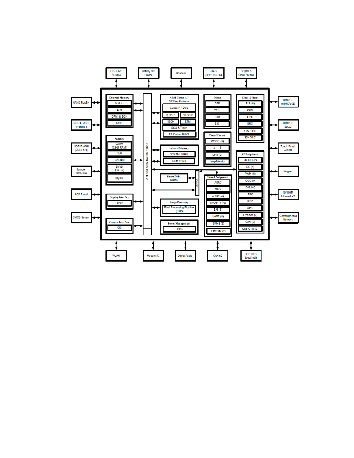
The figures below show block diagrams of the ConnectCore 6UL module and of the NXP i.MX6UL
application processor.
ConnectCore® 6UL Hardware Reference Manual
7
Page 8
About the ConnectCore® 6UL Block diagrams
ConnectCore 6UL module
ConnectCore® 6UL Hardware Reference Manual
8
Page 9
About the ConnectCore® 6UL Block diagrams
NXP i.MX6UL application processor
ConnectCore® 6UL Hardware Reference Manual
9
Page 10
About the ConnectCore® 6UL Power interfaces
Power interfaces
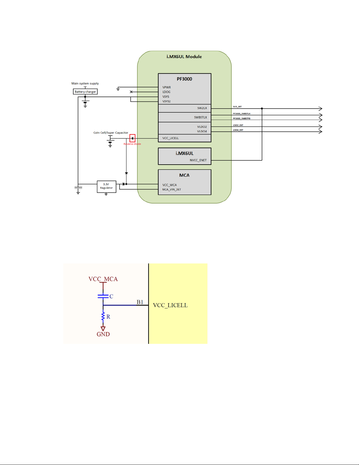
Power supply architecture
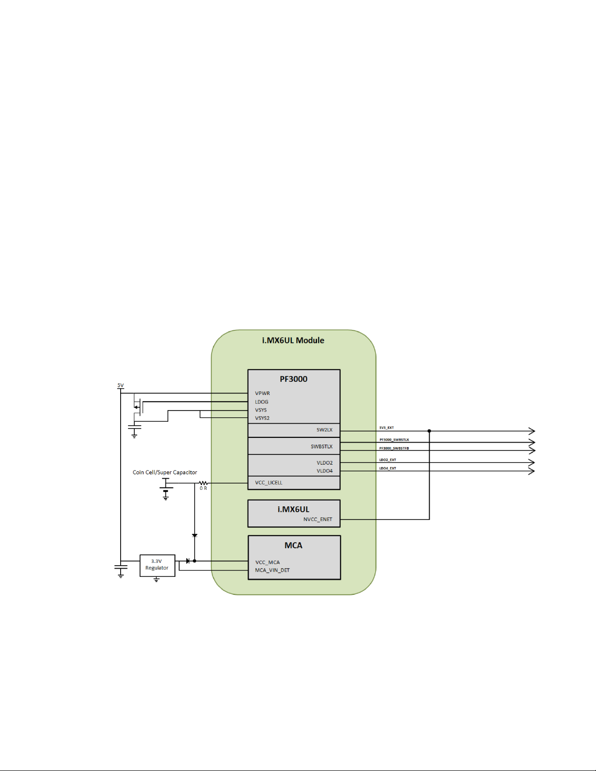
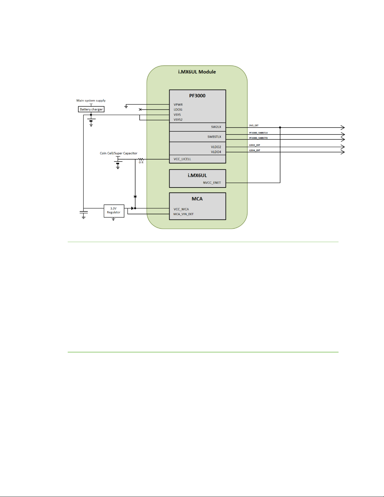
The ConnectCore 6UL requires a primary power supply input. This supply is the main power domain to
the on-module NXP PF3000 power management IC (PMIC), which generates all required supply
voltages for the module as well as the external interfaces. The system can be powered from voltages
up to 5.5V. See Powering the system from a nominal 5V power supply (4.5V to 5.5V) and Powering the
system for battery-powered applications (3.7V - 4.5V) for recommended power schemes for the
ConnectCore 6UL module.
The ConnectCore 6UL module has a dedicated pin for connecting a coin cell backup battery or
supercapacitor. You can enable a coin cell charger on the PMIC with Li-ion rechargeable batteries. This
backup battery or supercapacitor is mandatory if RTC time must persist after the module has been
disconnected from main power. You must also follow the recommended diode configuration as shown
in the diagrams below to make sure the module holds the system time.
If RTC time retention is not required, you can remove the circuitry from your design and connect the
3.3V voltage regulator directly to the VCC_MCA and MCA_VIN_DET pins.
Powering the system from a nominal 5V power supply (4.5V to 5.5V)
ConnectCore® 6UL Hardware Reference Manual
10
Page 11
About the ConnectCore® 6UL Power interfaces
Powering the system for battery-powered applications (3.7V - 4.5V)
Note In the implementations shown above, the coin cell/supercapacitor is connected to VCC_LICELL
pin of the ConnectCore 6UL module, allowing coin-cell charger applications. This VCC_LICELL
connection feeds the VSNVS regulator of the PMIC, which supplies the SNVS power domain of the
CPU. The VSNVS regulator derives its power from either VIN or the coin cell (VIN takes precedence),
and it cannot be disabled. This power domain allows some functionality of the CPU in low power mode
applications even when the main power supply of the system is removed. However, this connection
significantly increases the power consumption of the module in these low-power modes. This explains
the power consumption in power-off mode; see Global power consumption for more information
To optimize power management in coin cell applications:
Do not connect the coin cell/supercapacitor to the VCC_LICELL power domain. You must keep the
connection to VCC_MCA. This drastically reduces power consumption and extends the life of the
power supply. To preserve coin cell charger functionality, follow the instructions in the Coin cell
section.
The power architecture of the module is described in more detail below.
The PMIC generates the following power domains that are available on the module pads:
n Buck converters. Two buck regulators provide 3.3V:
l SW1A: 3V3_INT, powers several interfaces inside the module
l SW2: 3V3_EXT, free power line not used inside the module
n And another two buck regulators used for internal supply:
l SW1B: VDD_ARM_SOC_IN
l SW3: VCC_DDR3
ConnectCore® 6UL Hardware Reference Manual
11
Page 12
About the ConnectCore® 6UL Power interfaces
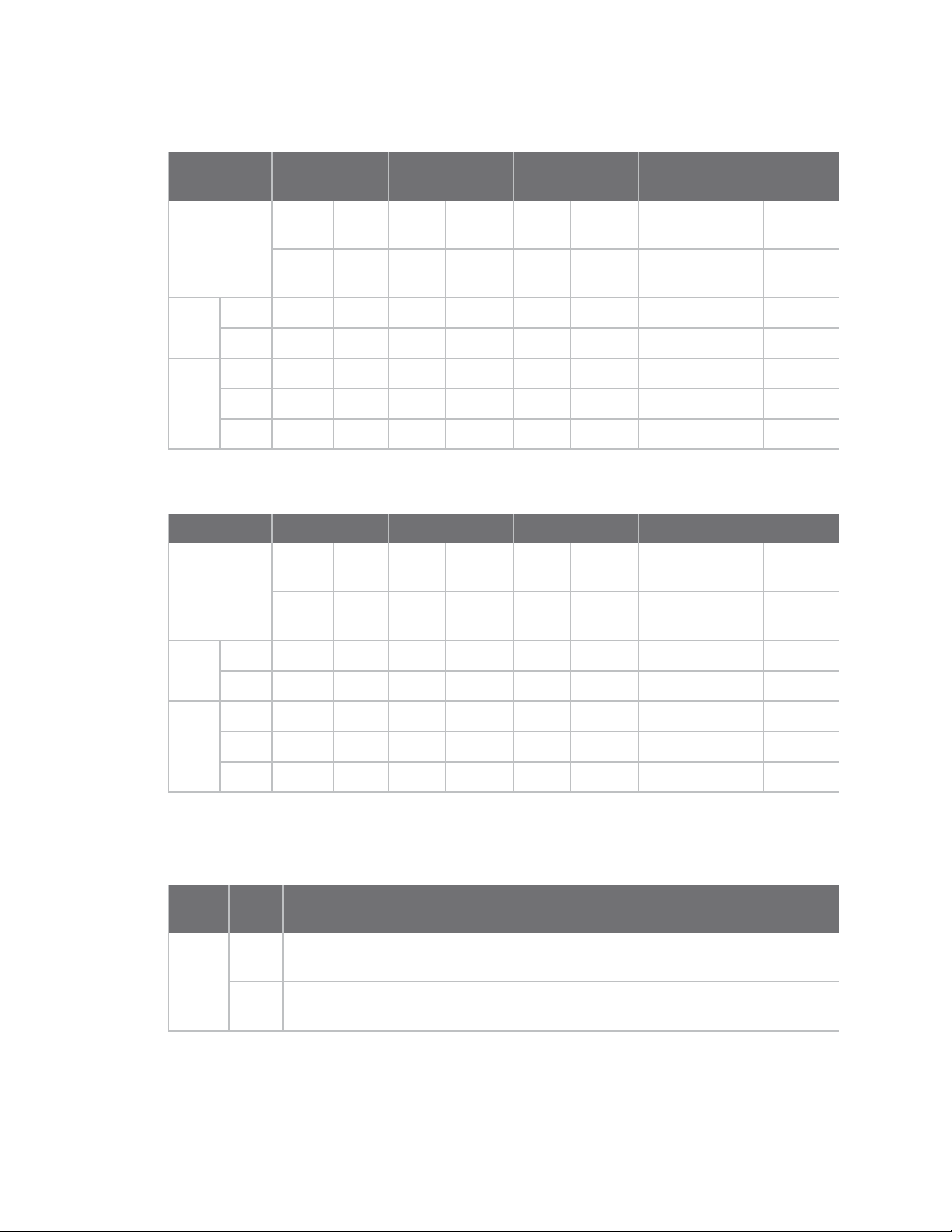
Quiescent
Power
domain
Regulator
type
Output
accuracy
Maximum
current
Dropout
voltage
(MAX)
Turn on
time
(MAX)
Turn
off time
(MAX)
current in
OFF mode
(TYP)
SW1A DC/DC +/-6.0 % 1.00 A - 500 us - -
SW2 DC/DC +/-6.0 % 1.25 A - 500 us - -
SW1B DC/DC +/-6.0 % 1.75 A - 500 us - -
SW3 DC/DC +/-6.0 % 1.5 A - 500 us - -
Note Maximum current includes both the module and the module carrier board consumption.
SW1: parameters specified at TA=-40 °C to 85 °C, VIN=VSW1xIN=3.6V, VSW1x=1.2 V, ISW1x=100 mA.
SW2: parameters specified at TA=-40 °C to 85 °C, VIN=VSW2IN=3.6V, VSW2=3.15 V, ISW2=100 mA.
SW3: parameters specified at TA=-40 °C to 85 °C, VIN=VSW3IN=3.6V, VSW3=1.5 V, ISW3=100 mA.
When powering up the SOM, PMIC OTP programming sets the ramp-up rate of all buck regulators to
12.5 mV/μs.
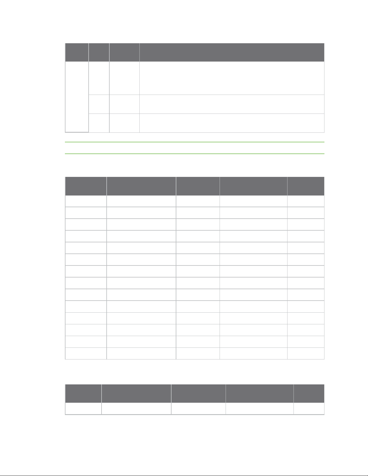
n LDO regulators. Four PMIC regulators are available; the module uses LDO1: VDDA_ADC_3P3.
LDO
Regulator
type
Output
accuracy
Maximum
current
Dropout
voltage
(MAX)
Turn on
time
(MAX)
Turn off
time
(MAX)
Quiescent
current in OFF
mode (TYP)
VLDO1 1.8-3.3V +/-3.0 % 0.100 A 60 mV 500 us 10 ms 13 uA
VLDO2 0.8-1.55V +/-3.0 % 0.250 A 60 mV 500 us 10 ms 13 uA
VLDO3 1.8-3.3V +/-3.0 % 0.100 A 60 mV 500 us 10 ms 13 uA
VLDO4 1.8-3.3V +/-3.0 % 0.350 A 60 mV 500 us 10 ms 13 uA
Note Maximum current includes both the module and the module carrier board consumption.
VLDO1 parameters specified at TA=-40 °C to 85 °C, VIN=3.6V, VLDO1IN=3.6V, VLDO1=3.3V, ILDO1=10
mA.
VLDO2 parameters specified at TA=-40 °C to 85 °C, VIN=3.6V, VLDO2IN=3.0V, VLDO2=1.55V, ILDO2=10
mA.
VLDO3 parameters specified at TA=-40 °C to 85 °C, VIN=3.6V, VLDO34IN=3.6V, VLDO3=3.3V, ILDO3=10
mA.
VLDO4 parameters specified at TA=-40 °C to 85 °C, VIN=3.6V, VLDO34IN=3.6V, VLDO4=3.3V, ILDO4=10
mA.
n Boost converter. The PMIC offers a boost regulator that is not used inside the module but that
is available in the pinout of the LGA version for customizations.
ConnectCore® 6UL Hardware Reference Manual
12
Page 13
About the ConnectCore® 6UL Power interfaces
Quiescent
current in
OFF mode
(TYP)
Power
domain
Regulator
type
Output
accuracy
Maximum
current
Dropout
voltage
(MAX)
Turn on
time
(MAX)
Turn
off time
(MAX)
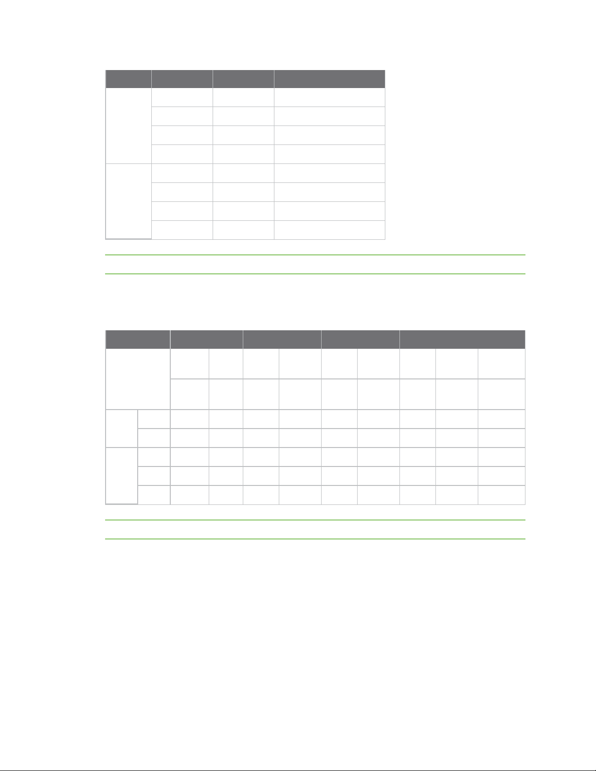
SWBST DC/DC -4.0% /
0.6 A - 2 ms - -
+3%
Note SWBST parameters specified at TA=-40 °C to 85 °C, VIN=VSWBSTIN=3.6V, VLSWBST=5.0V,
ISWBST=100 mA.
VSYS and VSYS2 are the supply inputs to the regulators and buck converters of the PMIC. Both inputs
are available on the module pads and can be connected to a single voltage input or to two different
voltages on systems that require high efficiency on the power system:
n VSYS powers SW1A, SW2, LDO1 and LDO34 (shared input for LDO3 and LDO4).
n VSYS2 powers SW1B, SW3 and LDO2.
The power management IC located on the module is responsible for generating all required i.MX6UL
processor supplies. Some of the I/O supplies are set on the module. See the following table:
Power domain Connection
NVCC_NAND 3V3_INT
NVCC_GPIO 3V3_INT
NVCC_SD1 3V3_INT
NVCC_UART 3V3_INT
NVCC_CSI 3V3_INT
NVCC_LCD 3V3_INT
One I/O voltage must be set externally and is left unconnected on the ConnectCore 6UL module:
NVCC_ENET. See the following table for operating range of NVCC_ENET:
Power domain Min Type Max
NVCC_ENET 1.65 V 1.8/2.8/3.3 V 3.6 V
As shown in the table above, the supply has a wide operating range. In order to provide the most costeffective and flexible solution for a given use case, the supplies listed in the table must be provided by
the carrier board integrating the ConnectCore 6UL module. However, PMIC 3.3V and LDO power rails
are dedicated power sources for supplying i.MX6UL power domains.
Note Electrical and timing characteristics of the processor (i.MX6UL industrial), PMIC (PF3000), and
MCA (KL03P24M48SF0) can be found in the corresponding datasheets, which are publicly available
from the manufacturer.
ConnectCore® 6UL Hardware Reference Manual
13
Page 14
About the ConnectCore® 6UL Power interfaces
System power-up sequence
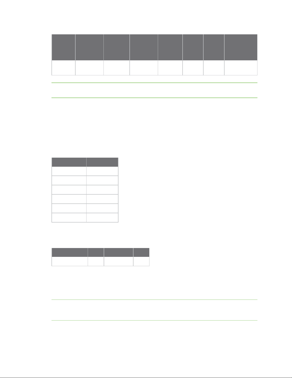
The ConnectCore 6UL can be configured to power-up the system in two different ways:
Power-up over power supply attach
Note This is the default power-up configuration of the ConnectCore 6UL.
In this mode, the SOM is completely powered-up as soon as the power supply is attached to the
system. When this happens, the PMIC and the MCA are the first components to be powered. VSYS
represents the PMIC input power line, while VCC_MCA is the MCA input power line. The MCA starts to
run as soon as it is powered, while the PMIC follows a fixed initialization process. The PMIC is switched
on by controlling the PWRON signal (the on-off control line of the PMIC), which is managed by the MCA.
The MCA turns on the PMIC after a user-programmable delay (50 ms by default).
Once the PMIC is switched on, another fixed initialization process starts and the PMIC regulators are
turned on following a sequence defined in its OTPs. Finally, the CPU reset line (POR_B_CPU), which is
also controlled by the MCA, is released. The following time diagram shows the power-up sequence in
this mode:
To optimize the power-up sequence, Digi suggest a configuration that controls the main input power
supply of the SOM (VSYS) through the PWR_ON line (e.g. through a power switch). For more
information, see the detailed hardware implementation in the ConnectCore 6ULSBCPro reference
design schematics. In this case, VSYS won't be enabled until the MCA drives the PWR_ON line high. The
following simplified time diagram illustrates this particular case:
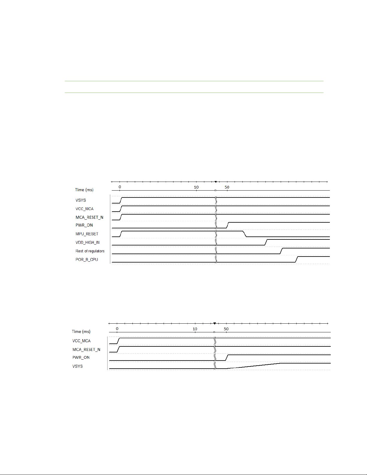
Power-up over PWR_IO
PWR_IO is the power on/off signal of the SOM, which is typically connected to a power button or any
other control peripheral/actuator. While in this mode, the power-up sequence will not start until an
event is capture on the PWR_IO line. See the simplified time diagram of this power-up mode below:
ConnectCore® 6UL Hardware Reference Manual
14
Page 15
About the ConnectCore® 6UL Power interfaces
Note This power-up mode is available in MCA firmware version 1.4. For more information, see the
ConnectCore 6UL software documentation.
Coin cell
Rechargeable coin cell/supercap
VCC_LICELL is the input power line of an always-on regulator of the PMIC (VSNVS) that feeds the lowpower mode circuitry of the CPU. By keeping this CPU power domain powered, the consumption of
the SOM increases significantly in this low-power mode. See Power supply architecture.
However, this connection is not required at all since the low-power mode functionality of the SOM is
supported by default by the on-module MCA. This means that the coin cell should only power the VCC_
MCA power domain (through the diode configuration explained in this chapter). By doing this, the coincell charger functionality is lost but the power consumption is drastically reduced.
If coin-cell charger functionality is mandatory, place a reverse diode between VCC_LICELL and the coin
cell to keep the low-power mode power consumption of the SOM under desirable values. This allows
current to flow from the SOM to the coin cell (charging) and blocks current going into VCC_LICELL line.
Note You must take into account the forward voltage drop of the diode for charging the coin cell.
ConnectCore® 6UL Hardware Reference Manual
15
Page 16
About the ConnectCore® 6UL Bootstrap
Digi has validated this hardware configuration with the Panasonic DB2J31400L diode. It's low reverse
leakage current (300 nA) is ideal for this low-power mode application.
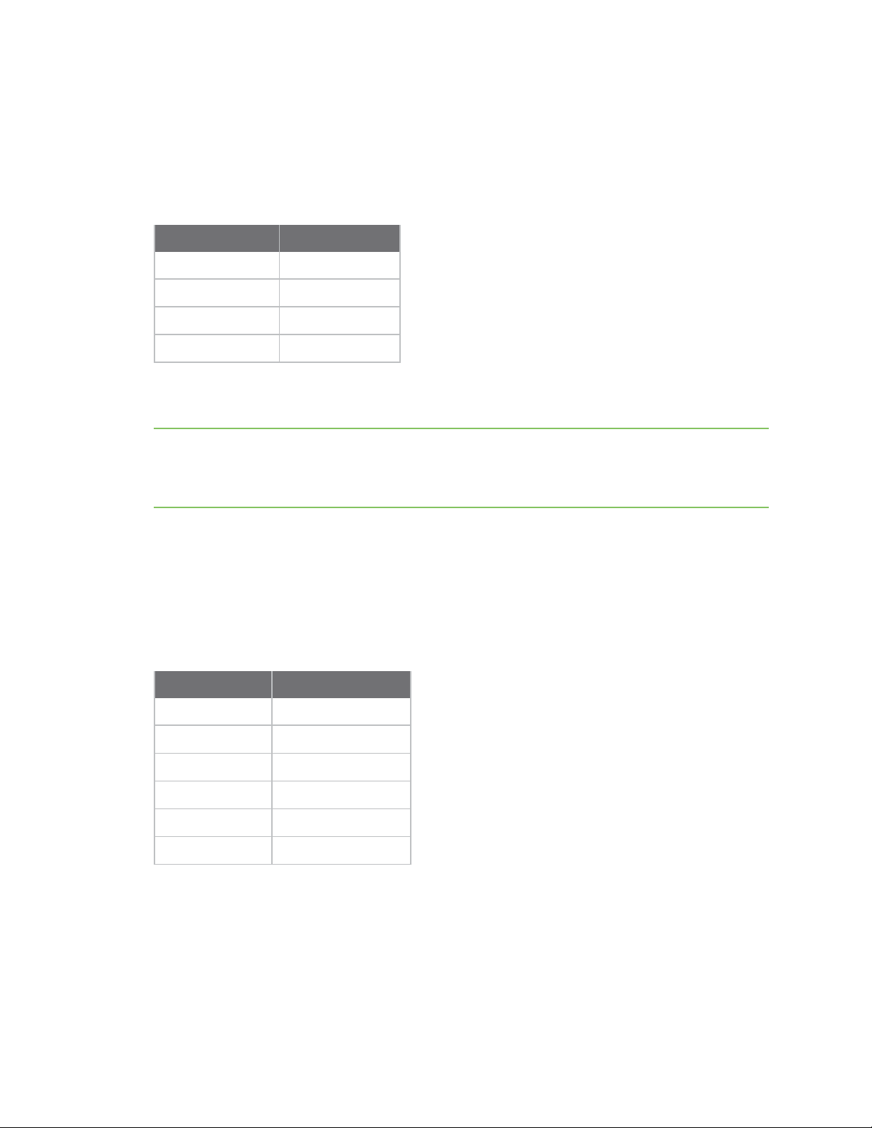
Non-rechargeable coin cell
For non-rechargeable coin cell applications, add the following RC circuit at the input of VCC_LICELL
pad (B1):
Electrical values of the passive components of the filter:
n C = 4.7 uF
n R = 47 kΩ
Bootstrap
The ConnectCore 6UL module can be configured to boot from different devices and interfaces as
determined by the Boot ROM. The configuration of the booting process of the CPU is done through:
ConnectCore® 6UL Hardware Reference Manual
16
Page 17
About the ConnectCore® 6UL Bootstrap
n BOOT_MODE register, which selects the boot mode of the processor.
n eFUSEs and/or GPIOs, which determine the boot configuration.
Four boot modes are available on the i.MX6UL processor. Selection between them is done through
BOOT_MODE[1:0] bits. The bits are externally configurable on two processor IOs, whose values are
latched during boot-up:
BOOT_MODE [1:0] Boot type
00 Boot from fuses
01 Serial downloader
10 Internal boot
11 Reserved
BOOT_MODE[0] and BOOT_MODE[1] are available on dedicated LGA pads on the module. However, on
the castellated pads only BOOT_MODE[1] is available.
Note BOOT_MODE[0] is set to 0 internally on the module through a 100K pull-down resistor. This
means that in applications using only the castellated pads of the module, the only boot modes
available are Boot from fuses and Internal boot. However, once Uboot is running, you can select a
different boot mode (like serial downloader).
Boot from fuses
Boot from fuses is the recommended boot mode for production purposes. When this boot mode is
selected, you must configure several parameters in order to select and configure the boot device of
the system. These parameters are configured through fuses, which are burned in order to set their
values. This means that the configuration is irreversible.
BOOT_CFG1 selects the boot device through BOOT_CFG1[7:4] bits:
BOOT_CFG1[7:4] Boot device
0000 NOR/OneNAND (EIM)
0001 QSPI
0011 Serial ROM (SPI)
010x SD/eSD/SDXC
011x MMC/eMMC
1xxx Raw NAND
There are many other registers that configure the different boot devices. For a complete description
of the booting configuration, refer to the NXP i.MX 6UltraLite Applications Processor Reference
Manual (Chapter 8: System Boot).
ConnectCore® 6UL Hardware Reference Manual
17
Page 18
About the ConnectCore® 6UL Bootstrap
Internal boot
Internal boot is the recommended boot mode for development purposes. When this boot mode is
selected, the selection and configuration of the booting process is done through the same registers
used when booting from fuses. However, this time the values of some registers are overridden using
multiple GPIOs, which are latched during power-up.
The following configuration is done internally in the ConnectCore 6UL module in order to enable
booting from the NAND memory:
Bootstrap configuration Corresponding GPIO Default configuration
BOOT_CFG2[1] LCD_DATA9 100K pull-down
BOOT_CFG2[2] LCD_DATA10 100K pull-down
BOOT_CFG2[3] LCD_DATA11 100K pull-up
BOOT_CFG2[4] LCD_DATA12 100K pull-down
BOOT_CFG2[5] LCD_DATA13 100K pull-up
BOOT_CFG2[6] LCD_DATA14 100K pull-down
BOOT_CFG2[7] LCD_DATA15 100K pull-down
You must also set up BOOT_CFG1[7:0] register when booting from the internal on-module NAND when
Internal boot mode is selected. It must be configured externally (outside the module) as shown in the
following table:
Bootstrap configuration Corresponding GPIO Configuration
BOOT_CFG1[0] LCD_DATA0 0
BOOT_CFG1[1] LCD_DATA1 0
BOOT_CFG1[2] LCD_DATA2 0
BOOT_CFG1[3] LCD_DATA3 0
BOOT_CFG1[4] LCD_DATA4 1
BOOT_CFG1[5] LCD_DATA5 0
BOOT_CFG1[6] LCD_DATA6 0
BOOT_CFG1[7] LCD_DATA7 1
Digi recommends you use 10K pull-up and pull-down resistors to configure each line.
The BOOT_CFG1 and BOOT_CFG2 register lines are not dedicated lines of the CPU. This means that
the values of these lines are latched during the power-up, but have a different functionality once the
system is up and running. In this case, these lines belong to the LCD interface. In order to protect the
value of these registers while the system is booting, Digi recommends you use a protection circuitry
as shown in sheet 3 of 7, "Boot selection," of the ConnectCore 6UL reference designs. See Design files.
ConnectCore® 6UL Hardware Reference Manual
18
Page 19
About the ConnectCore® 6UL Wireless interfaces
CAUTION! BOOT_CFG4[7:0] is available on LCD_DATA[23:16]. Make sure BOOT_CFG4[7]
(LCD_DATA23) is not kept high while booting. This bootstrap pin is configuring the "infinite
loop enable" at the start of the boot ROM. If this pin is high while booting, the infinite loop is
enabled and the system will not boot.
Serial downloader
You can use the serial downloader boot mode for device recovery. The serial downloader allows you to
download a program image to the chip through a USB or UART serial connection. When any of the
standard boot modes is selected but the booting process doesn’t succeed (for instance due to wrong
booting device or corrupted images) the CPU automatically jumps to the serial downloader boot
mode.
Wireless interfaces
The ConnectCore 6UL System-on-module combines a wireless local area network (WLAN) and
Bluetooth dual solution to support IEEE802.11 a/b/g/n/ac WLAN standards and Bluetooth 4.2, enabling
seamless integration of WLAN/Bluetooth and Low Energy technology. Digi also offers a non-wireless
variant of the ConnectCore 6UL module.
The following sections include specifications for the wireless interfaces available on the ConnectCore
6UL module.
WLAN IEEE 802.11a/b/g/n/ac
The 2.4 GHz band on the ConnectCore 6UL module supports 20/40 MHz bandwidths, and the 5 GHz
band supports 20/40/80 MHz bandwidths. The following sections specify the performance of the WLAN
IEEE 802.11a/b/g/n/ac interface on the ConnectCore 6UL module.
Modulation and data rates
The following tables list modulation values for the ConnectCore 6UL module, which supports the
following WLAN standards:
Mode
802.11b DBPSK 1 Mbps
Modulation & coding
DQPSK 2 Mbps
CCK 5.5 Mbps
CCK 11 Mbps
Rate
ConnectCore® 6UL Hardware Reference Manual
19
Page 20

About the ConnectCore® 6UL Wireless interfaces
Mode
802.11ga BPSK-1/2 6 Mbps
802.11n BPSK-1/2 MCS0
Modulation & coding
BPSK-3/4 9 Mbps
QPSK-1/2 12 Mbps
QPSK-3/4 18 Mbps
16QAM-1/2 24 Mbps
16QAM-3/4 36 Mbps
64QAM-2/3 48 Mbps
64QAM-3/4 54 Mbps
QPSK-1/2 MCS1
QPSK-3/4 MCS2
16QAM-1/2 MCS3
16QAM-3/4 MCS4
64QAM-2/3 MCS5
Rate
64QAM-3/4 MCS6
64QAM-5/6 MCS7
802.11ac BPSK-1/2 MCS0
QPSK-1/2 MCS1
QPSK-3/4 MCS2
16QAM-1/2 MCS3
16QAM-3/4 MCS4
64QAM-2/3 MCS5
64QAM-3/4 MCS6
64QAM-5/6 MCS7
256QAM-3/4 MCS8
256QAM-5/6 MCS9
Note Rates MCS8 & MCS9 are only available in receive mode.
ConnectCore® 6UL Hardware Reference Manual
20
Page 21
About the ConnectCore® 6UL Wireless interfaces
Data rate (Mbps) - Non Short Guard Interval (Non-SGI)
Data rate
(Mbps) 802.11b 802.11ga 802.11n 802.11ac
Modulation DBPSK CCK BPSK-
1/2
1
Mbps11Mbps6Mbps54Mbps
2.4
GHz
5 GHz HT20 6 54 6.5 65 6.5 65
Data rate (Mbps) - Short Guard Interval (SGI)
Mode
Modulation DBPSK CCK BPSK-
2.4
GHz
HT20 1 11 6 54 6.5 65 6.5 65
HT40 13.5 135 13.5 135 180
HT40 13.5 135 13.5 135 180
HT80 29.3 292.5 390
802.11b 802.11ga 802.11n 802.11ac
1/2
1
Mbps11Mbps6Mbps54Mbps
HT20 1 11 6 54 7.2 72.2 7.2 72.2
HT40 15 150 15 150 200
64QAM3/4
64QAM3/4
BPSK1/2
MCS0 MCS7 MCS0 MCS7 MCS9
BPSK1/2
MCS0 MCS7 MCS0 MCS7 MCS9
64QAM5/6
64QAM5/6
BPSK1/2
BPSK1/2
64QAM5/6
64QAM5/6
256QAM5/6
256QAM5/6
5 GHz HT20 6 54 7.2 72.2 7.2 72.2
HT40 15 150 15 150 200
HT80 32.5 325 433.3
RF channels
The ConnectCore 6UL module supports the following frequency bands:
RF
band
2.4
GHz
Ch.BWCh.
spacing Channel number (Center freq. MHz)
20
MHz
40
MHz
5 MHz 1(2412), 2(2417), 3(2422), 4(2427), 5(2432), 6(2437), 7(2442), 8(2447), 9
5 MHz 3(2422), 11(2462)
(2452), 10(2457), 11(2462), 12(2467), 13(2472), 14(2484)
ConnectCore® 6UL Hardware Reference Manual
21
Page 22
About the ConnectCore® 6UL Wireless interfaces
RF
band
5 GHz 20
Note Dependent upon regulatory bodies.
2.4 GHz
2.4 GHz band
channel #
1 2412 ✔ ✔ ✔
2 2417 ✔ ✔ ✔
Ch.BWCh.
spacing Channel number (Center freq. MHz)
20 MHz 36(5180), 40(5200), 44(5220), 48(5240), 52(5260), 56(5280), 60(5300),
MHz
40
MHz
80
MHz
40 MHz 38(5190), 46(5230), 54(5270), 62(5310), 102(5510), 110(5550), 118
80 MHz 42(5210), 58(5290), 106(5530), 122(5610), 138(5690), 155(5775)
Center frequency
(MHz)
64(5320), 100(5500), 104(5520), 108(5540), 112(5560), 116(5580), 120
(5600), 124(5620), 128(5640), 132(5660), 136(5680), 140(5700), 144
(5720), 149(5745), 153(5765), 157(5785), 161(5805), 165(5825)
(5590), 126(5630), 134(5670), 142(5710), 151(5755), 159(5795)
EUROPE
(ETSI)
NORTH AMERICA
(FCC) JAPAN
3 2422 ✔ ✔ ✔
4 2427 ✔ ✔ ✔
5 2432 ✔ ✔ ✔
6 2437 ✔ ✔ ✔
7 2442 ✔ ✔ ✔
8 2447 ✔ ✔ ✔
9 2452 ✔ ✔ ✔
10 2457 ✔ ✔ ✔
11 2462 ✔ ✔ ✔
12 2467 ✔ No ✔
13 2472 ✔ No ✔
14 2484 No No 802.11b only
5 GHz
5 GHz band
channel # Center frequency (MHz) EUROPE (ETSI) NORTH AMERICA (FCC) JAPAN
36 5180 Indoors ✔ ✔
ConnectCore® 6UL Hardware Reference Manual
22
Page 23

About the ConnectCore® 6UL Wireless interfaces
5 GHz band
channel # Center frequency (MHz) EUROPE (ETSI) NORTH AMERICA (FCC) JAPAN
40 5200 Indoors ✔ ✔
44 5220 Indoors ✔ ✔
48 5240 Indoors ✔ ✔
52 5260 Indoors / DFS / TPC DFS DFS / TPC
56 5280 Indoors / DFS / TPC DFS DFS / TPC
60 5300 Indoors / DFS / TPC DFS DFS / TPC
64 5320 Indoors / DFS / TPC DFS DFS / TPC
100 5500 DFS / TPC DFS DFS / TPC
104 5520 DFS / TPC DFS DFS / TPC
108 5540 DFS / TPC DFS DFS / TPC
112 5560 DFS / TPC DFS DFS / TPC
116 5580 DFS / TPC DFS DFS / TPC
120 5600 DFS / TPC DFS DFS / TPC
124 5620 DFS / TPC DFS DFS / TPC
128 5640 DFS / TPC DFS DFS / TPC
132 5660 DFS / TPC DFS DFS / TPC
136 5680 DFS / TPC DFS DFS / TPC
140 5700 DFS / TPC DFS DFS / TPC
149 5745 SRD ✔ No Access
153 5765 SRD ✔ No Access
157 5785 SRD ✔ No Access
161 5805 SRD ✔ No Access
165 5825 SRD ✔ No Access
Note
DFS = Dynamic Frequency Selection
TPC = Transmit Power Control
SRD = Short Range Devices 25 mW max power
Transmit power
The following table lists nominal transmit power values for the ConnectCore 6UL module.
Note Nominal powers are subject to regulatory domain regulations.
ConnectCore® 6UL Hardware Reference Manual
23
Page 24
About the ConnectCore® 6UL Wireless interfaces
RF band Channel BW Standard Output power (dBm)
2.4 GHz 20 MHz 802.11b 18 (1Mbps) - 18 (11Mbps)
20 MHz 802.11g 18 (6Mbps) - 14 (54Mbps)
20 MHz 802.11n/ac 17 (MCS0) - 13 (MCS7)
40 MHz 802.11n/ac 15 (MCS0) - 13 (MCS7)
5 GHz 20 MHz 802.11a 13 (6Mbps) - 11 (54Mbps)
20 MHz 802.11n/ac 15 (MCS0) - 8 (MCS7)
40 MHz 802.11n/ac 12 (MCS0) - 7 (MCS7)
80 MHz 802.11ac 9 (MCS0) - 4 (MCS7)
Note Due to manufacturing tolerance, these nominal output powers may be reduced up to 3 dB.
Receive sensitivity
The following table lists typical receive sensitivity values for the ConnectCore 6UL module.
Mode 802.11b 802.11ga 802.11n 802.11ac
Modulation DBPSK CCK BPSK-
1/2
1
Mbps11Mbps6Mbps54Mbps
2.4
GHz
5 GHz HT20 - - -86 -72 -86 -67 -82 -64 -
Note Specification is subject to change.
HT20 -90 -84 -85 -69 -84 -65 -82 -64 -
HT40 - - - - -79 -61 -79 -61 -54
HT40 - - - - -79 -61 -79 -61 -54
HT80 - - - - - - -76 -58 -51
64QAM3/4
BPSK1/2
MCS0 MCS7 MCS0 MCS7 MCS9
64QAM5/6
BPSK1/2
64QAM5/6
256QAM5/6
Antenna ports
The ConnectCore 6UL module has two antenna ports: one on the module via a dedicated
U.FLconnector, and another on the LGA pads. Both antenna ports support WLAN and Bluetooth
functionality. You can use the control signal RF1_INT/nEXT to select between the on-module antenna
port (U.FLconnector) and the external antenna port (LGA pad). This control signal has a 10K pull-up
populated on the module, which means that the on-module antenna port (U.FL connector) is active by
default. Pulling RF1_INT/nEXTlow activates the external antenna port and disables the on-module
antenna port.
ConnectCore® 6UL Hardware Reference Manual
24
Page 25

About the ConnectCore® 6UL Parallel display
Bluetooth
The ConnectCore 6UL module supports both Bluetooth and Bluetooth Low Energy protocols:
n Bluetooth 4.2; backwards compatible with Bluetooth 1.X, 2.X + Enhanced Data Rate, Bluetooth
3.X, Bluetooth 4.0 and Bluetooth 4.1. Bluetooth class 1 and class 2 power-level transmissions
n Integrated WLAN-Bluetooth coexistence
See Bluetooth certification for more information.
RF control signals
The following signals are not supported by the current firmware of the WLAN/Bluetooth transceiver:
n WLAN_RF_KILL# (pad B17)
n BT_RF_KILL# (pad B18)
n WLAN_LED (pad B19)
n BT_LED (pad B20)
Parallel display
The ConnectCore 6UL provides a 24-bit RGB LCD interface. The following table shows the color
mapping of this interface when configured to work in 16/18/24 bits.
Signal name Description 16-bit 18-bit 24-bit
LCD_DATA0 Display data line 0 B[0] B[0] B[0]
LCD_DATA1 Display data line 1 B[1] B[1] B[1]
LCD_DATA2 Display data line 2 B[2] B[2] B[2]
LCD_DATA3 Display data line 3 B[3] B[3] B[3]
LCD_DATA4 Display data line 4 B[4] B[4] B[4]
LCD_DATA5 Display data line 5 G[0] B[5] B[5]
LCD_DATA6 Display data line 6 G[1] G[0] B[6]
LCD_DATA7 Display data line 7 G[2] G[1] B[7]
LCD_DATA8 Display data line 8 G[3] G[2] G[0]
LCD_DATA9 Display data line 9 G[4] G[3] G[1]
LCD_DATA10 Display data line 10 G[5] G[4] G[2]
LCD_DATA11 Display data line 11 R[0] G[5] G[3]
LCD_DATA12 Display data line 12 R[1] R[0] G[4]
LCD_DATA13 Display data line 13 R[2] R[1] G[5]
LCD_DATA14 Display data line 14 R[3] R[2] G[6]
ConnectCore® 6UL Hardware Reference Manual
25
Page 26
About the ConnectCore® 6UL Microcontroller Assist™
Signal name Description 16-bit 18-bit 24-bit
LCD_DATA15 Display data line 15 R[4] R[3] G[7]
LCD_DATA16 Display data line 16 R[4] R[0]
LCD_DATA17 Display data line 17 R[5] R[1]
LCD_DATA18 Display data line 18 - R[2]
LCD_DATA19 Display data line 19 - R[3]
LCD_DATA20 Display data line 20 - R[4]
LCD_DATA21 Display data line 21 - R[5]
LCD_DATA22 Display data line 22 - R[6]
LCD_DATA23 Display data line 23 - R[7]
Note 24-bit displays can be connected to an 18-bit parallel LCD bus. For this, the six most significant
data bits of the display are connected to the 18-bit LCD bus. The remaining two least significant data
bits of the display can be connected in two ways:
n Connected either to GND or VCC. In this case, it's not possible to reach a full black or white.
n Connected to the lower bits of the same color. In this case, full black and white can be reached,
but some color gradients are lost.
Microcontroller Assist™
The Microcontroller Assist, orMCA, is a small microcontroller that is deeply integrated into the design
of the ConnectCore 6UL module. It assists the i.MX6UL processor with advanced operations related to
power management, security, and system reliability. The functionality provided by the MCA includes:
n Advanced power management such as power key button, wake up sources, and PMIC control
in low power.
n Peripheral extensions such as RTC, watchdog, and tamper pins.
The MCA and the i.MX6UL are connected through an I2C interface and an interrupt line. The
microcontroller provides up to 20 general purpose IOs that can be configured with different modes to
provide functionality such as digital input/output or ADC.
The i.MX6UL can update the MCA firmware over the I2C bus. See the MCAsoftware documentation for
additional information about this process.
ConnectCore® 6UL Hardware Reference Manual
26
Page 27
About the ConnectCore® 6UL Microcontroller Assist™
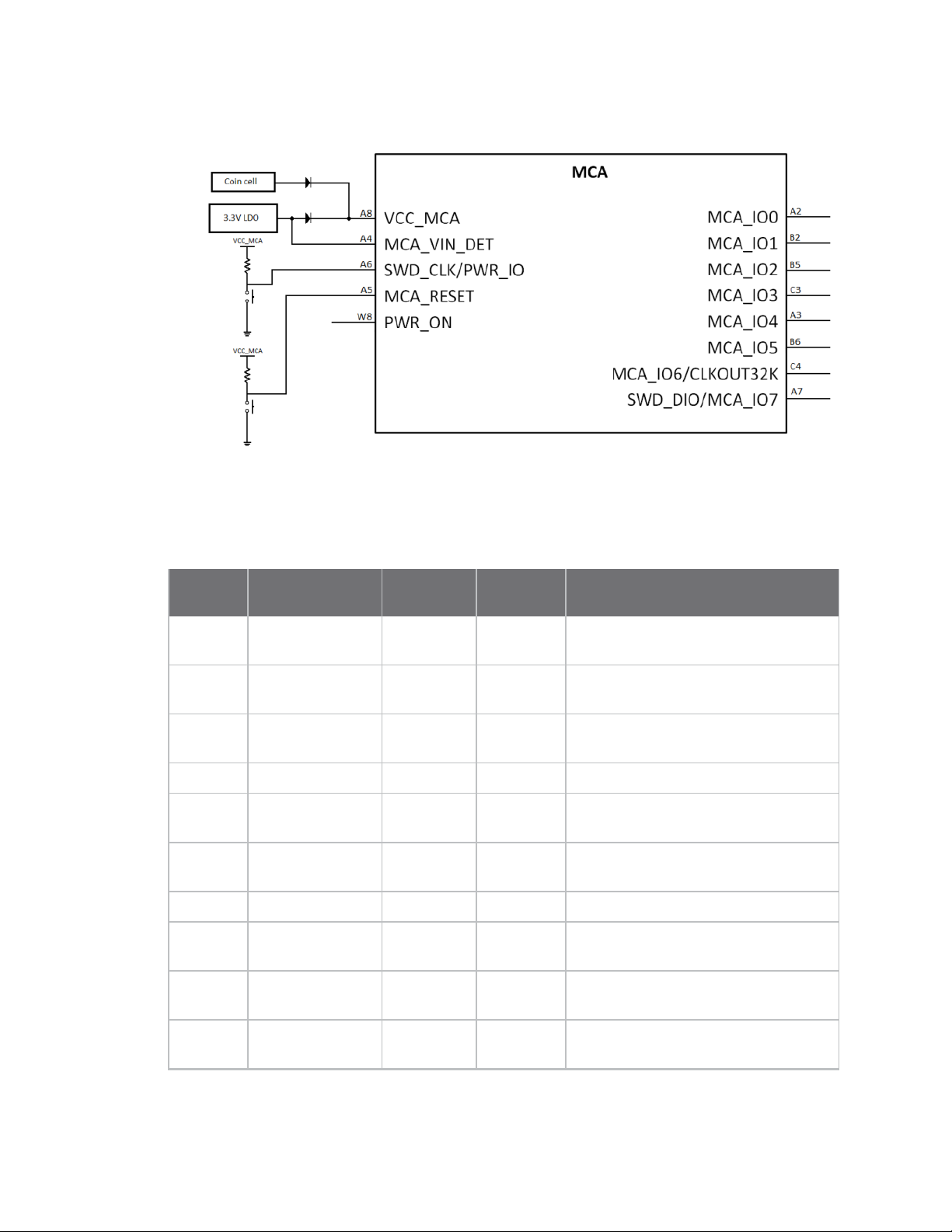
ConnectCore 6UL module lines related to the MCA
Pin
number Pin name
A2 MCA_IO0 Bi-
A3 MCA_IO4 Bi-
A4 MCA_VIN_DET Input Analog Input voltage detection line. Connect to
A5 MCA_RESET Input Digital Reset input line, active low.
A6 SWD_CLK/PWR_IOInput Digital Power on/off input line, active low. SWD
A7 SWD_DIO/MCA_
IO7
A8 VCC_MCA Input Analog Input power supply of the MCA.
B2 MCA_IO1 Bi-
Pin
direction Type Definition
directional
directional
Bidirectional
directional
Digital and
analog
Digital and
analog
Digital General purpose Input/Ouput. SWD
Digital and
analog
General purpose Input/Output.
General purpose Input/Output.
VCC_MCA.
interface clock line.
interface data line.
General purpose Input/Output.
B5 MCA_IO2 Bi-
directional
B6 MCA_IO5 Bi-
directional
ConnectCore® 6UL Hardware Reference Manual
Digital General purpose Input/Output.
Digital and
analog
General purpose Input/Output.
27
Page 28

About the ConnectCore® 6UL Microcontroller Assist™
Pin
number Pin name
C3 MCA_IO3 Bi-
C4 MCA_
IO6/CLKOUT32K
Pin
direction Type Definition
directional
Bidirectional
Digital and
analog
Digital General purpose Input/Output. 32KHz
General purpose Input/Output.
clock output.
W8 PWR_ON Output Digital Output power on/off line. Set to low
level during power off.
Reset control
Asserting and de-asserting the MCA_RESET line wakes the ConnectCore 6UL module from any power
mode (suspend/power off). Then, the microcontroller executes the programmed firmware.
The MCA, in cooperation with the PMIC, controls the reset line of the i.MX6UL processor (POR_B). The
MCA_RESET pin is the main reset input of the ConnectCore 6UL module. This pin is a pseudo opendrain with an internal pull up. Asserting the MCA_RESET line low sets the MCA into reset state, and it
remains in this state until the line is de-asserted.
During system initialization, the MCA performs the following actions:
n Asserts the PWR_ON line low for a configurable number of milliseconds (0-255 ms with a
default value of 50ms). This powers the PMIC off, switching off all regulated outputs of the
PMIC. You can disable this power cycle by setting the timer to 0.
n Asserts the PWR_ONline high to power the system on (assuming it was asserted low before).
n Keeps POR_B asserted low for a configurable number of miliseconds.
n Asserts the POR_B line high to start the execution of the firmware on the i.MX6UL processor.
Note ThePOR_B line is also connected to the PMIC. The PMIC won't release this line until it is
switched on andthe entire starting sequence is finished (a few ms after the latest regulator is
turned on). This means that even if the MCA releases the reset line before the PMIC is ready,
the CPU won't go out of reset. This occurs on the ConnectCore 6UL module: the MCA releases
the CPU reset line by putting the MPU_RESET linehigh butthere's a delay since this GPIO goes
high until the POR_B_CPU line goes high. The delay occurs because the PMIC is still not
completely initialized.
The following time diagram represents the reset sequence. You can configure the reset timing.
Default values are as follows:
n tr
: 50 ms
1
n tr
: 2 ms
2
ConnectCore® 6UL Hardware Reference Manual
28
Page 29
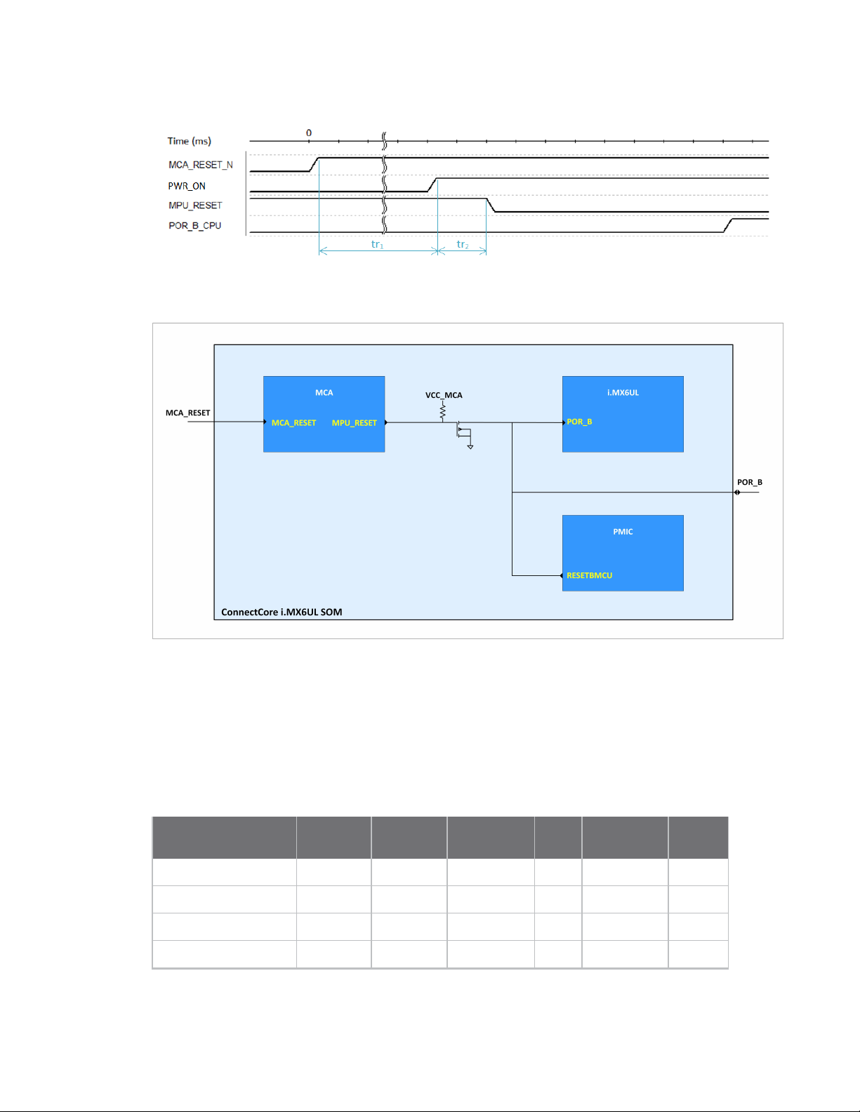
About the ConnectCore® 6UL Microcontroller Assist™
SeeSystem power-up sequencefor more information about the power-up sequence of
theConnectCore 6UL.
See the MCAsoftware documentation for additional information on the configuration of the MCA.
IOs
The ConnectCore 6UL MCA provides up to eight configurable IOs.
Since the general purpose IOs do not incorporate internal pull-ups or pull-downs, you may have to add
the components to the exterior of the module carrier board.
The following table lists all available MCA IOs with capabilities and module pad:
PAD
MCA IO
MCA_IO0 A2/76 ✔
MCA_IO1 B2
MCA_IO2/EXT_VREF B5
MCA_IO3 C3
LGA/CS* Digital I/O IRQ capable ADC 32KHz clock 1.2 Vref
✔ ✔
✔ ✔ ✔
✔ ✔
✔ ✔
✔
ConnectCore® 6UL Hardware Reference Manual
29
Page 30

About the ConnectCore® 6UL Microcontroller Assist™
PAD
MCA IO
LGA/CS* Digital I/O IRQ capable ADC 32KHz clock 1.2 Vref
MCA_IO4 A3/75
MCA_IO5 B6
MCA_IO6/CLKOUT32K C4
SWD_DIO/MCA_IO7 A7/71
* CS = castellated pads
✔ ✔
✔
✔
✔
✔
✔
✔
Digital IOs
All MCA IOs can be configured as digital inputs/outputs, which are powered from the MCA_VCC power
rail.
The digital outputs preserve the output value set in all operating modes, except in power off and coin
cell modes where the IOs are reconfigured to high impedance state to preserve power.
Note Since the general purpose IOs do not incorporate internal pull-ups or pull-downs, you may need
to add the components to the exterior of the module carrier board.
MCA IRQs
You can configure the MCA IOs as interrupt inputs, using the MCA software to configure the active
edge of the interrupt (rising, falling, or both). The firmware provides a configurable debounce filter for
each GPIO that improves noise immunity and filters rebounds on push buttons. When one or more
MCA IRQs are activated, the MCA interrupts the main processor through the corresponding IRQ line,
signaling the active IRQs in the IRQ status registers. The IRQ inputs can wake the system from any
low power mode (suspend or power off).
See the MCA software documentation for additional information about how to configure and access
the MCA IRQ lines.
Analog to digital converter
You can configure up to five MCA IOs as Analog to Digital channels in addition to the ones provided by
the i.MX6UL CPU. The index of the MCA ADC channels corresponds to the index of the MCA IO. This
means that the ADC channel 0 corresponds to the MCA_IO0, the ADC channel 1 to the MCA_IO1, the
ADC channel 2 to the MCA_IO2, and so on.
The result of the ADC conversion for a given input voltage is inversely proportional to the reference
voltage of the ADC. For the MCA ADCs, the reference voltagecorresponds to the VCC_MCA voltage.
(Note that the i.MX6UL ADCs have a different reference voltage.) The MCA ADC provides 12-bit of
resolution with right-justified, unsigned format output. These ADCs are suitable for low-frequency
sampling(under 10 Hz). For higher frequency sampling, Digi recommends the CPU ADC channels. You
can configure the MCA ADC lines to act as an analog window comparator and generate an IRQ
depending on the voltage level in the input. This feature allows applications to be notified of this event
instead of needing to periodically poll the input for its value.
See the MCA software documentation for additional information about how to configure and access
the MCA IRQ lines.
ConnectCore® 6UL Hardware Reference Manual
30
Page 31

About the ConnectCore® 6UL Microcontroller Assist™
External voltage reference
The MCA_IO2/EXT_VREF pin provides an accurate voltage reference of 1.2V that can be used to
provide a reference voltage for sensors and/or analog devices (such as comparators or ADCs).
When this pin is used as external reference voltage or as the internal reference of the MCA analog-todigital converter,an external capacitor of 100nF must be connectedbetween the pin and ground and
as close as possible to the module pad.
The default configuration of the MCA_IO2/EXT_VREF pin is as a general IO. You must use software to
configure the pin for external voltage reference.
See the MCA software documentation for additional information about how to control the function of
this pin.
Note that the voltage reference continues normal operation in low power modes (suspend and power
off). Therefore, if the voltage reference is enabled during normal operation but is not required for low
power operation, Digi recommends using the software to disable it before entering low power in order
to minimize the power consumption, and re-enable it when resuming normal operation.
External 32KHz clock output
The MCA_IO6/CLKOUT32K pin is a 32.768 Hz square wave output that can be used as clock input by
peripherals requiring a low-frequency, high-accuracy clock.
Note The default configuration of theMCA_IO6/CLKOUT32K pin is as IO. You must use software to
configure the pin as 32KHz clock output. See the MCAsoftware documentation for additional
information about how to control the function of this pin.
Watchdog
The MCA implements a watchdog timer in its firmware. The MCA watchdog resets the system, or only
the i.MX6UL CPU, if the software running on the main processor fails to execute properly and does not
reset the watchdog timer on time.
The main featuresof the MCA watchdog include:
ConnectCore® 6UL Hardware Reference Manual
31
Page 32

About the ConnectCore® 6UL Microcontroller Assist™
n Configurable timeout between 1 and 255 seconds.
n Configurableto generate interrupt or system reset.
n Configurable to generate full-system reset (including the MCA itself) or CPU-only reset. Full-
system reset can include a PMIC off/on, depending on the device configuration.
See the MCAsoftware documentation for additional information about how to configure and access
the watchdog timer.
Real-time clock
The MCA implements a Real-Time Clock (RTC) in its firmware. The i.MX6UL CPU internal RTCs are
disabled by default because the MCA RTC is preferred due to its superior power consumption
efficiency. To preserve the date during power-off, you must connect a coin cell battery following the
design notes provided in Power supply architecture. You must also connect the MCA line MCA_VIN_
DET following the design guidelines inPower supply architecture in order to detect power loss and
automatically switch to RTC mode.
The main features of the MCA RTC include:
n Date/time registers to keep the system time (backed up by the coin cell battery).
n Programmable alarm to generate an interrupt. This alarm can be used to wake the system
from low power modes (suspend and power off).
See the MCAsoftware documentation for additional information about how to configure and access
the watchdog timer.
Tamper support
The tamper interface provides a mechanism to detect any unauthorized attempt to access the
system, such as the opening of the enclosure. The tamper support included in the ConnectCore 6UL is
implemented in the MCA with the following capabilities:
n Configure up to two tamper interfaces, each with an optional digital output.
n Rely on tamper detection event in power-off and coin cell (battery backup) modes.
n Register tamper event(s) in the non-volatile memory of the MCA.
n Alert the host CPU when a tamper event occurs.
n Respond to a tamper attack with actions such as erasing a critical data partition of the flash.
Tamper pins
The ConnectCore 6UL supports up to two tamper interfaces (tamper0 and tamper1). Each interface
has an associated IO (tamper pin) used to detect the tamper event (through a voltage transition on
the IO) and, optionally, an output IO (tamper output) that can be used to enable or disable peripherals,
for instance to cut the power of a peripheral. The IOs of each tamper interface can be configured
independently and have the following configuration options:
n The MCA IO used for tamper detection, from the available MCA IOs that are IRQ-capable.
n The active level (tampering) of the tamper input.
n The MCA IO used as tamper output, when enabled, that is activated when a tamper condition
has not been acknowledged.
n The logic level that is set in the tamper output when a tamper event occurs.
ConnectCore® 6UL Hardware Reference Manual
32
Page 33

About the ConnectCore® 6UL Microcontroller Assist™
The MCA IO table provides information about the capabilities of the MCA IO pins so you can easily
identify suitable IOs to be used as tamper inputs. Any MCA IO pin can be configured as tamper output.
Tamper pin configuration
To learn more about tamper pin configuration, see Tamper detection interface in the software
documentation.
Note Tamper pins coming from the i.MX6UL processor are not supported. Tamper functionality on the
module is only implemented on MCA I/Os.
Power management
The MCA plays a key role in the power management activities of the ConnectCore 6UL module. In
cooperation with the i.MX6UL processor, the MCA controls the power states of the PMIC and provides
multiple wake up sources to transition between power modes. It also allocates dedicated signals to
capture power events and indicate the system power state, allowing you to control external power
sources and indicators.
Power modes
The module provides four different power operating modes: ON/RUN, OFF, SUSPEND, and COIN-CELL.
The following figure shows the state diagram and the events to switch between states.
ConnectCore® 6UL Hardware Reference Manual
33
Page 34

About the ConnectCore® 6UL Microcontroller Assist™
W4PK mode
You can configure boot mode using the mca_config_tool –boot_mode option.
If ‘boot on power’ (BOP) is chosen, the module will enter in ON state as soon as power is applied.
If ‘wait for power key’ (W4PK) is chosen, the module will wait for a PWR_IO press before entering in
ON state when power is applied.
ON/RUN mode
The module enters the ON state after a power-on or system-reset event.
In this mode, the PMIC is running at full power so all voltage regulators are generating the nominal
voltage for this mode. The CPU reset line is de-asserted and the processor is running at normal speed,
performing DVFS if the system was configured to do so. In this state, the PWR_ON line is asserted
high, indicating that the module is ON.
ConnectCore® 6UL Hardware Reference Manual
34
Page 35

About the ConnectCore® 6UL Microcontroller Assist™
Note that the specific state of the regulators (on/off) and the voltage in this mode are controlled by
the firmware running on the i.MX6UL processor. The PMIC starts with the default settings configured
on the OTP area, but once the software takes control itapplies the specific configuration
implemented in the firmware.
SUSPEND mode
The suspend mode (also known as suspend-to-RAM mode) is the low-power mode that allows the
module to preserve RAM content. When the module enters SUSPEND, the following actions take place:
n The processor goes into low power, disabling as much functionality as possible and keeping
active only the peripherals configured to wake the system from SUSPEND.
n The DDR memory is set to self-refresh mode to preserve its contents while reducing power
consumption.
n The PMIC goes into standby mode, configuring the regulators in the configured mode (on, off,
with a different voltage compared to ON state).
n The MCA goes into sleep mode, keeping active the peripherals that always run in low power
modes (like the RTC) and those configured to wake up the system (such as IRQs and power IO).
MCA GPIOs configured as outputs also keep their value.
OFF mode
The module enters OFF mode after a power-off event. In this mode:
n The PMIC is set to the OFF state and all the voltage regulators, except VSNVS, are switched off.
n The PWR_ON line is asserted low, indicating that the module is in OFF state.
n The MCA goes into sleep mode, keeping active the peripherals that always run in low-power
modes (like the RTC) and those configured to wake up the system (such as IRQs and power IO).
COIN-CELL mode
In COIN-CELL mode, the module only powers the MCA from the coin-cell battery, leaving the rest of
the module power inputs switched off. In this mode, the MCA remains in sleep mode, updating the RTC
and monitoring the following events:
n Tamper events that would be registered in the NVRAM memory of the MCA and would assert
the Tamper output if enabled.
n Power in MCA_VIN_DET, which indicates that there is sufficient voltage to generate a power-
on event.
Power IO signal/Power button
The MCA provides a signal (PWR_IO) to detect external events that trigger a transition between the
different power modes described in Power modes. The pin has wake-up interrupt/event capabilities, it
is active low, and it does not provide an internal pull-up. (The pull-up resistor must be added externally
if required.) This signal is ideal for connecting a power button or the output of a peripheral that
controls the power state of the module and its transitions. The firmware provides a configurable
debounce filter to improve noise immunity and filter rebounds on push buttons. When the PWR_IO
signal is asserted low, one of the following events occurs:
n If the duration of the assertion is short (time configurable by the user) the system will trigger
an interrupt that, commonly, indicates the host processor that the system should enter
suspend state.
ConnectCore® 6UL Hardware Reference Manual
35
Page 36

About the ConnectCore® 6UL CryptoAuthentication device
n If the low-pulse duration is long enough (again, time-configurable by the user) the system
triggers the power off interrupt, to tell the host processor to start a transition to OFF state.
n If the system does not enter OFF state before a configurable guard timer expires, the MCA will
automatically set the OFF state unless the user explicitly cancels it by writing to the mca_
cancel_pwroff entry in the sysfilesystem.
Digi recommends you use an external pull-up resistor of 100K to VCC_MCA in this SWD_CLK/PWR_IO
line.
MCA_VIN_DET signal
The on-module MCA is powered from a dedicated external power rail, VCC_MCA. As recommended in
the reference designs (see Power supply architecture), this power supply is provided by an external
3.3V regulator. If the system requires system time to be kept when there is no power, you must use a
coin-cell battery to power the MCA while it keeps the RTC up to date in low-power mode. The MCA
uses the MCA_VIN_DET input to monitor the input voltage and automatically switch to RTC mode to
keep the system time and save power. Follow the design guidelines provided inPower supply
architecture to apply the proper voltage to MCA_VIN_DET when there is a coin-cell battery in the
system and when there is not.
MCA_VIN_DET is a digital line, not analog. This means that the transition time between high and low
values is crucial to optimize the time the system takes to switch to RTC mode. Digi recommends you
ensure a fast discharge of this signal to allow a quick fall time.
MCA firmware update
The i.MX6UL processor can update the firmware of the MCA. See the MCAsoftware documentation for
additional information about the MCA firmware update process.
CryptoAuthentication device
The ConnectCore 6UL module includes an Atmel CryptoAuthentication Device. This is a highly secure
cryptographic co-processor with secure hardware-based key storage. It includes the following
features:
n Performs high-speed public key (PKI) algorithms (ECDSA and ECDH). NIST standard P256
elliptic curve support.
n SHA-256 hash algorithm with HMAC option.
n 256-bit key length.
n Storage for up to 16 keys.
n Two high-endurance monotonic counters.
n Guaranteed unique 72-bit serial number.
n Internal High-quality FIPS Random Number Generator (RNG).
n 10 Kb EEPROM memory.
See the software documentation for information about supported cryptoauthentication features.
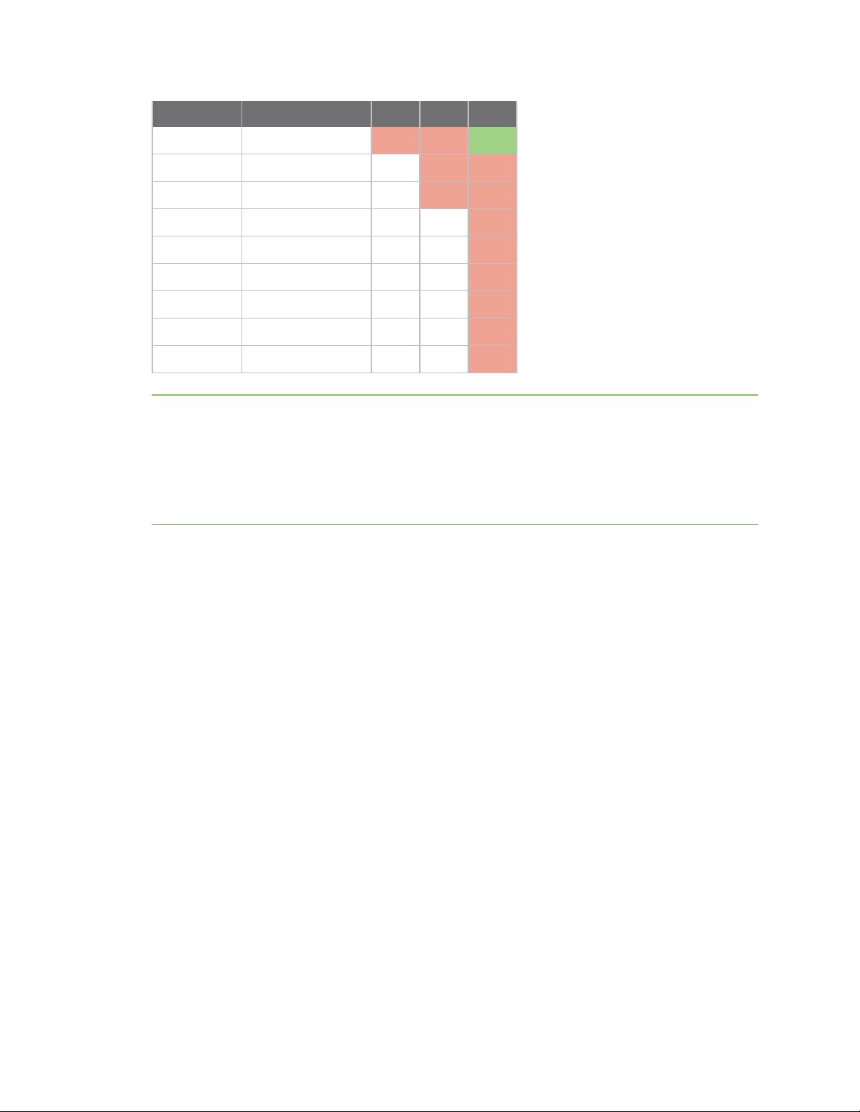
Module pinout - general layout
The ConnectCore 6UL module has a mixed pad structure. The module provides 245 LGA pins, 76 of
them connected to the peripheral castellated pads. The general layout can be found on the following
diagram:
ConnectCore® 6UL Hardware Reference Manual
36
Page 37

About the ConnectCore® 6UL Module pinout - general layout
n White cells: LGA pads
n Orange cells: castellated pads
Note Pad A1 is unconnected. This pad is meant for module-orientation purposes; its shape is square,
whereas all other pads are circular. Pad A1 should not be soldered down to a corresponding pad on
the carrier board.
ConnectCore® 6UL Hardware Reference Manual
37
Page 38

ConnectCore® 6UL Hardware Reference Manual 38
External signals and pin multiplexing
The following tables provide the pinout information of the ConnectCore 6UL module. For additional information related to the signals listed in the table,
refer to the NXP i.MX6UL technical documentation.
Note The Digi ConnectCore Smart IOmux tool can dramatically simplify pin configuration and resolution. You can enter the list of interfaces required by
your project and use the Smart IOmux graphical interface to mock up configuration options, resulting in full pin assignment and device tree snippets that
match your desired functionality. See the Smart IOmux User Guide for more information and download instructions.
The microprocessor used on this module, like all CMOS devices, can be driven into a latch-up condition if any I/O pin is driven outside of its
associated power rail. Care must be taken to:
n Never drive an I/O pin beyond its positive rail or below ground.
n Never drive an I/O pin from an external power source during the power-on or reset sequences.
n Never hot-swap the module or interrupt its ground connection to external circuitry.
Latch-up is a condition that can cause excessive current draw and result in excessive heating of the microprocessor or its power supplies. This
excessive heating can permanently damage the microprocessor and/or its supporting components.
When you use an external supply on the carrier board supporting the ConnectCore 6UL module, make sure this supply is NOT back driving
i.MX6UL I/Os while their power rails are not enabled. For example, this can happen when an external 3.3V supply is available on the carrier
board and this supply powers components driven by i.MX6UL I/Os. In this case, Digi recommends you enable the external power supply after
internal 3.3V is enabled, or add the necessary protection circuitry to avoid back voltage (leakage).
Castellated pad signals and multiplexing
Note The ConnectCore 6UL module is using the I2C1 port internally to connect the MCA and Power Management IC (PMIC). Digi does not recommend
using I2C1 externally.
Page 39

ConnectCore® 6UL Hardware Reference Manual 39
ConnectCore
Castellated
pad
ConnectCore
6UL pad
6UL signal
name i.MX6UL pad name Multiplexing
Power
group Comments
1 / B1 CPAD1 VCC_LICELL
2 / C1 CPAD2 VSYS
3 / D1 CPAD3 VPWR
4 / E1 CPAD4 LDOG
5 / F1 CPAD5 GND
6 / G1 CPAD6 VSYS
7 / H1 CPAD7 VSYS2
8 / J1 CPAD8 GND
9 / K1 CPAD9 3V3_EXT
-
-
-
-
-
-
-
-
-
VCC_
LICELL
VSYS Input power
VPWR Input power
LDOG PMIC
-
VSYS Input power
VSYS2 Input power
-
3V3_EXT Output
Coin cell
supply
line
line
external LDO
gate control
line
line
line
power line
Page 40

ConnectCore® 6UL Hardware Reference Manual 40
ConnectCore
Castellated
pad
ConnectCore
6UL pad
6UL signal
name i.MX6UL pad name Multiplexing
Power
group Comments
10 / L1 CPAD10 LCD_DATA8
LCD_DATA08
ALT0: LCDIF_DATA08
ALT1: SPDIF_IN
VCC_
LCD
ALT2:
ALT3: CSI_DATA16
ALT4: EIM_DATA0
ALT5: GPIO3_IO13
ALT6: SRC_BT_CFG08
ALT7:
ALT8: FLEXCAN1_TX
11 / M1 CPAD11 LCD_DATA9
LCD_DATA09
ALT0: LCDIF_DATA09
ALT1: SAI3_MCLK
VCC_
LCD
ALT2:
ALT3: CSI_DATA17
ALT4: EIM_DATA1
ALT5: GPIO3_IO14
ALT6: SRC_BT_CFG09
ALT7:
ALT8: FLEXCAN1_RX
12 / N1 CPAD12 VCC_ENET VCC_
ENET
100K pulldown on
module
Input power
line
Page 41

ConnectCore® 6UL Hardware Reference Manual 41
ConnectCore
Castellated
pad
13 / P1 CPAD13 POR_B VDDIO 10K pull-up
ConnectCore
6UL pad
6UL signal
name i.MX6UL pad name Multiplexing
Power
group Comments
on module
connected
to VDD_
SNVS
Input reset
line of the
module
(active low)
14 / R1 CPAD14 CSI_MCLK
15 / T1 CPAD15 CSI_PIXCLK
CSI_MCLK
CSI_PIXCLK
ALT0: CSI_MCLK
ALT1: USDHC2_CD_B
ALT2: NAND_CE2_B
ALT3: I2C1_SDA
ALT4: EIM_CS0_B
ALT5: GPIO4_IO17
ALT6: SNVS_VIO_5_CTL
ALT7:
ALT8: UART6_TX
ALT0: CSI_PIXCLK
ALT1: USDHC2_WP
ALT2: NAND_CE3_B
ALT3: I2C1_SCL
ALT4: EIM_OE
ALT5: GPIO4_IO18
ALT6: SNVS_HP_VIO_5
ALT7:
ALT8: UART6_RX
NVCC_
CSI
NVCC_
CSI
I2C1_SDA is
not available
on this pad
I2C1_SCL is
not available
on this pad
Page 42

ConnectCore® 6UL Hardware Reference Manual 42
ConnectCore
Castellated
pad
ConnectCore
6UL pad
6UL signal
name i.MX6UL pad name Multiplexing
Power
group Comments
16 / U1 CPAD16 CSI_DATA1
17 / V1 CPAD17 CSI_HSYNC
18 / W1 CPAD18 GPIO1_5
CSI_DATA01
CSI_HSYNC
GPIO1_IO05
ALT0: CSI_DATA03
ALT1: USDHC2_DATA1
ALT2: SIM1_PORT1_SVEN
ALT3: ECSPI2_SS0
ALT4: EIM_AD01
ALT5: GPIO4_IO22
ALT6: SAI1_MCLK
ALT7:
ALT8: UART5_RX
ALT0: CSI_HSYNC
ALT1: USDHC2_CMD
ALT2: SIM1_PORT1_PD
ALT3: I2C2_SCL
ALT4: EIM_LBA_B
ALT5: GPIO4_IO20
ALT6: PWM8_OUT
ALT7:
ALT8: UART6_CTS_B
ALT0: ENET2_REF_CLK2
ALT1: PWM4_OUT
ALT2: USB_OTG2_ID
ALT3: CSI_FIELD
ALT4: USDHC1_VSELECT
ALT5: GPIO1_IO05
ALT6: ENET2_1588_EVENT0_OUT
ALT7:
ALT8: UART5_RX
NVCC_
CSI
NVCC_
CSI
NVCC_
GPIO
Page 43

ConnectCore® 6UL Hardware Reference Manual 43
ConnectCore
Castellated
pad
ConnectCore
6UL pad
6UL signal
name i.MX6UL pad name Multiplexing
Power
group Comments
19 / Y1 CPAD19 BOOT_MODE1 VDD_
SNVS
20 / AA2 CPAD20 CSI_DATA0
21 / AA3 CPAD21 CSI_VSYNC
CSI_DATA00
CSI_VSYNC
ALT0: CSI_DATA02
ALT1: USDHC2_DATA0
ALT2: SIM1_PORT1_RST_B
ALT3: ECSPI2_SCLK
ALT4: EIM_AD00
ALT5: GPIO4_IO21
ALT6: SRC_INT_BOOT
ALT7:
ALT8: UART5_TX
ALT0: CSI_VSYNC
ALT1: USDHC2_CLK
ALT2: SIM1_PORT1_CLK
ALT3: I2C2_SDA
ALT4: EIM_RW
ALT5: GPIO4_IO19
ALT6: PWM7_OUT
ALT7:
ALT8: UART6_RTS_B
NVCC_
CSI
NVCC_
CSI
Page 44

ConnectCore® 6UL Hardware Reference Manual 44
ConnectCore
Castellated
pad
ConnectCore
6UL pad
6UL signal
name i.MX6UL pad name Multiplexing
Power
group Comments
22 / AA4 CPAD22 CSI_DATA2
23 / AA5 CPAD23 CSI_DATA3
24 / AA6 CPAD24 UART5_TX
CSI_DATA02
CSI_DATA03
UART5_TX_DATA
ALT0: CSI_DATA04
ALT1: USDHC2_DATA2
ALT2: SIM1_PORT1_TRXD
ALT3: ECSPI2_MOSI
ALT4: EIM_AD02
ALT5: GPIO4_IO23
ALT6: SAI1_RX_SYNC
ALT7:
ALT8: UART5_RTS_B
ALT0: CSI_DATA05
ALT1: USDHC2_DATA3
ALT2: SIM2_PORT1_PD
ALT3: ECSPI2_MISO
ALT4: EIM_AD03
ALT5: GPIO4_IO24
ALT6: SAI1_RX_BCLK
ALT7:
ALT8: UART5_CTS_B
ALT0: UART5_TX
ALT1: ENET2_CRS
ALT2: I2C2_SCL
ALT3: CSI_DATA14
ALT4: CSU_CSU_ALARM_AUT00
ALT5: GPIO1_IO30
ALT6:
ALT7:
ALT8: ECSPI2_MOSI
NVCC_
CSI
NVCC_
CSI
NVCC_
UART
Page 45

ConnectCore® 6UL Hardware Reference Manual 45
ConnectCore
Castellated
pad
ConnectCore
6UL pad
6UL signal
name i.MX6UL pad name Multiplexing
Power
group Comments
25 / AA7 CPAD25 UART5_RX
26 / AA8 CPAD26 USB_OTG1_P
27 / AA9 CPAD27 USB_OTG1_N
28 / AA10 CPAD28 GND
29 / AA11 CPAD29 USB_OTG1_
VBUS
30 / AA12 CPAD30 GPIO1_4
UART5_RX_DATA
USB_OTG1_DP
USB_OTG1_DN
-
USB_OTG1_VBUS
GPIO1_IO04
ALT0: UART5_RX
ALT1: ENET2_COL
ALT2: I2C2_SDA
ALT3: CSI_DATA15
ALT4: CSU_CSU_INT_DEB
ALT5: GPIO1_IO31
ALT6:
ALT7:
ALT8: ECSPI2_MISO
ALT0: ENET1_REF_CLK1
ALT1: PWM3_OUT
ALT2: USB_OTG1_PWR
ALT3: ANATOP_24M_OUT
ALT4: USDHC1_RESET_B
ALT5: GPIO1_IO04
ALT6: ENET2_1588_EVENT0_IN
ALT7:
ALT8: UART5_TX
NVCC_
UART
-
USB_
VBUS
NVCC_
GPIO
USB
differential
data line
USB
differential
data line
Input power
line
Page 46

ConnectCore® 6UL Hardware Reference Manual 46
ConnectCore
Castellated
pad
ConnectCore
6UL pad
6UL signal
name i.MX6UL pad name Multiplexing
Power
group Comments
31 / AA13 CPAD31 GPIO1_0
32 / AA14 CPAD32 GPIO1_1
33 / AA15 CPAD33 JTAG_MOD
GPIO1_IO00
GPIO1_IO01
JTAG_MOD
ALT0: I2C2_SCL
ALT1: GPT1_CAPTURE1
ALT2: USB_OTG1_ID
ALT3: ENET1_REF_CLK1
ALT4: MQS_RIGHT
ALT5: GPIO1_IO00
ALT6: ENET1_1588_EVENT0_IN
ALT7: SRC_SYSTEM_RESET
ALT8: WDOG3_WDOG_B
ALT0: I2C2_SDA
ALT1: GPT1_COMPARE1
ALT2: USB_OTG1_OC
ALT3: ENET2_REF_CLK2
ALT4: MQS_LEFT
ALT5: GPIO1_IO01
ALT6: ENET1_1588_EVENT0_OUT
ALT7: SRC_EARLY_RESET
ALT8: WDOG1_WDOG_B
ALT0: SJC_MOD
ALT1: GPT2_CLK
ALT2: SPDIF_OUT
ALT3: XTALOSC_REF_CLK_25M
ALT4: CCM_PMIC_READY
ALT5: GPIO1_IO10
ALT6: SDMA_EXT_EVENT00
ALT7:
ALT8:
NVCC_
GPIO
NVCC_
GPIO
NVCC_
GPIO
10K pulldown on
module
Page 47

ConnectCore® 6UL Hardware Reference Manual 47
ConnectCore
Castellated
pad
ConnectCore
6UL pad
6UL signal
name i.MX6UL pad name Multiplexing
Power
group Comments
34 / AA16 CPAD34 JTAG_TMS
35 / AA17 CPAD35 USB_OTG2_P
36 / AA18 CPAD36 USB_OTG2_N
37 / AA19 CPAD37 GPIO1_7
JTAG_TMS
USB_OTG2_DP
USB_OTG2_DN
GPIO1_IO07
ALT0: SJC_TMS
ALT1: GPT2_CAPTURE1
ALT2: SAI2_MCLK
ALT3: CCM_CLKO1
ALT4: CCM_WAIT
ALT5: GPIO1_IO11
ALT6: SDMA_EXT_EVENT01
ALT7:
ALT8: EPIT1_OUT
ALT0: ENET1_MDC
ALT1: ENET2_MDC
ALT2: USB_OTG_HOST_MODE
ALT3: CSI_PIXCLK
ALT4: USDHC2_CD_B
ALT5: GPIO1_IO07
ALT6: CCM_STOP
ALT7:
ALT8: UART1_RTS_B
NVCC_
GPIO
USB
differential
data line
USB
differential
data line
NVCC_
GPIO
Page 48

ConnectCore® 6UL Hardware Reference Manual 48
ConnectCore
Castellated
pad
ConnectCore
6UL pad
6UL signal
name i.MX6UL pad name Multiplexing
Power
group Comments
38 / AA20 CPAD38 GPIO1_6
39 / Y21 CPAD39 JTAG_TDO
40 / W21 CPAD40 JTAG_TCK
GPIO1_IO06
JTAG_TDO
JTAG_TCK
ALT0: ENET1_MDIO
ALT1: ENET2_MDIO
ALT2: USB_OTG_PWR_WAKE
ALT3: CSI_MCLK
ALT4: USDHC2_WP
ALT5: GPIO1_IO06
ALT6: CCM_WAIT
ALT7: CCM_REF_EN_B
ALT8: UART1_CTS_B
ALT0: SJC_TDO
ALT1: GPT2_CAPTURE2
ALT2: SAI2_TX_SYNC
ALT3: CCM_CLKO2
ALT4: CCM_STOP
ALT5: GPIO1_IO12
ALT6: MQS_RIGHT
ALT7:
ALT8: EPIT2_OUT
ALT0: SJC_TCK
ALT1: GPT2_COMPARE2
ALT2: SAI2_RX_DATA
ALT3:
ALT4: PWM7_OUT
ALT5: GPIO1_IO14
ALT6: OSC32K_32K_OUT
ALT7:
ALT8: SIM2_POWER_FAIL
NVCC_
GPIO
NVCC_
GPIO
NVCC_
GPIO
Page 49

ConnectCore® 6UL Hardware Reference Manual 49
ConnectCore
Castellated
pad
ConnectCore
6UL pad
6UL signal
name i.MX6UL pad name Multiplexing
Power
group Comments
41 / V21 CPAD41 JTAG_TDI
42 / U21 CPAD42 JTAG_nTRST
43 / T21 CPAD43 UART2_TX
JTAG_TDI
JTAG_TRST_B
UART2_TX_DATA
ALT0: SJC_TDI
ALT1: GPT2_COMPARE1
ALT2: SAI2_TX_BCLK
ALT3:
ALT4: PWM6_OUT
ALT5: GPIO1_IO13
ALT6: MQS_LEFT
ALT7:
ALT8: SIM1_POWER_FAIL
ALT0: SJC_TRSTB
ALT1: GPT2_COMPARE3
ALT2: SAI2_TX_DATA
ALT3:
ALT4: PWM8_OUT
ALT5: GPIO1_IO15
ALT6: ANATOP_24M_OUT
ALT7:
ALT8:CAAM_RNG_OSC_OBS
ALT0: UART2_TX
ALT1: ENET1_TDATA02
ALT2: I2C4_SCL
ALT3: CSI_DATA06
ALT4: GPT1_CAPTURE1
ALT5: GPIO1_IO20
ALT6:
ALT7:
ALT8: ECSPI3_SS0
NVCC_
GPIO
NVCC_
GPIO
NVCC_
UART
Page 50

ConnectCore® 6UL Hardware Reference Manual 50
ConnectCore
Castellated
pad
ConnectCore
6UL pad
6UL signal
name i.MX6UL pad name Multiplexing
Power
group Comments
44 / R21 CPAD44 UART2_RX
45 / P21 CPAD45 GND
46 / N21 CPAD46 UART2_CTS#
47 / M21 CPAD47 UART2_RTS#
UART2_RX_DATA
-
UART2_CTS_B
UART2_RTS_B
ALT0: UART2_RX
ALT1: ENET1_TDATA03
ALT2: I2C4_SDA
ALT3: CSI_DATA07
ALT4: GPT1_CAPTURE2
ALT5: GPIO1_IO21
ALT6:
ALT7: SJC_DONE
ALT8: ECSPI3_SCLK
ALT0: UART2_CTS_B
ALT1: ENET1_CRS
ALT2: FLEXCAN2_TX
ALT3: CSI_DATA08
ALT4: GPT1_COMPARE2
ALT5: GPIO1_IO22
ALT6:
ALT7: SJC_DE_B
ALT8: ECSPI3_MOSI
ALT0: UART2_RTS_B
ALT1: ENET1_COL
ALT2: FLEXCAN2_RX
ALT3: CSI_DATA09
ALT4: GPT1_COMPARE3
ALT5: GPIO1_IO23
ALT6:
ALT7: SJC_FAIL
ALT8: ECSPI3_MISO
NVCC_
UART
-
NVCC_
UART
NVCC_
UART
Page 51

ConnectCore® 6UL Hardware Reference Manual 51
ConnectCore
Castellated
pad
ConnectCore
6UL pad
6UL signal
name i.MX6UL pad name Multiplexing
Power
group Comments
48 / L21 CPAD48 ENET1_RX_
DATA0
49 / K21 CPAD49 ENET1_RX_EN
50 / J21 CPAD50 ENET1_RX_ER
ENET1_RX_DATA0
ENET1_RX_EN
ENET1_RX_ER
ALT0: ENET1_RDATA00
ALT1: UART4_RTS_B
ALT2: PWM1_OUT
ALT3: CSI_DATA16
ALT4: FLEXCAN1_TX
ALT5: GPIO2_IO00
ALT6: KPP_ROW00
ALT7:
ALT8: USDHC1_LCTL
ALT0: ENET1_RX_EN
ALT1: UART5_RTS_B
ALT2: OSC32K_32K_OUT
ALT3: CSI_DATA18
ALT4: FLEXCAN2_TX
ALT5: GPIO2_IO02
ALT6: KPP_ROW01
ALT7:
ALT8: USDHC1_VSELECT
ALT0: ENET1_RX_ER
ALT1: UART7_RTS_B
ALT2: PWM8_OUT
ALT3: CSI_DATA23
ALT4: EIM_CRE
ALT5: GPIO2_IO07
ALT6: KPP_COL03
ALT7:
ALT8: GPT1_CAPTURE2
NVCC_
ENET
NVCC_
ENET
NVCC_
ENET
Page 52

ConnectCore® 6UL Hardware Reference Manual 52
ConnectCore
Castellated
pad
ConnectCore
6UL pad
6UL signal
name i.MX6UL pad name Multiplexing
Power
group Comments
51 / H21 CPAD51 ENET1_TX_
DATA1
52 / G21 CPAD52 ENET1_TX_EN
53 / F21 CPAD53 ENET1_TX_
CLK
ENET1_TX_DATA1
ENET1_TX_EN
ENET1_TX_CLK
ALT0: ENET1_TDATA01
ALT1: UART6_CTS_B
ALT2: PWM5_OUT
ALT3: CSI_DATA20
ALT4: ENET2_MDIO
ALT5: GPIO2_IO04
ALT6: KPP_ROW02
ALT7:
ALT8: WDOG1_WDOG_RST_B_DEB
ALT0: ENET1_TX_EN
ALT1: UART6_RTS_B
ALT2: PWM6_OUT
ALT3: CSI_DATA21
ALT4: ENET2_MDC
ALT5: GPIO2_IO05
ALT6: KPP_COL02
ALT7:
ALT8: WDOG2_WDOG_RST_B_DEB
ALT0: ENET1_TX_CLK
ALT1: UART7_CTS_B
ALT2: PWM7_OUT
ALT3: CSI_DATA22
ALT4: ENET1_REF_CLK1
ALT5: GPIO2_IO06
ALT6: KPP_ROW03
ALT7:
ALT8: GPT1_CLK
NVCC_
ENET
NVCC_
ENET
NVCC_
ENET
Page 53

ConnectCore® 6UL Hardware Reference Manual 53
ConnectCore
Castellated
pad
ConnectCore
6UL pad
6UL signal
name i.MX6UL pad name Multiplexing
Power
group Comments
54 / E21 CPAD54 ENET1_RX_
DATA1
55 / D21 CPAD55 ENET1_TX_
DATA0
56 / C21 CPAD56 LCD_CLK
ENET1_RX_DATA1
ENET1_TX_DATA0
LCD_CLK
ALT0: ENET1_RDATA01
ALT1: UART4_CTS_B
ALT2: PWM2_OUT
ALT3: CSI_DATA17
ALT4: FLEXCAN1_RX
ALT5: GPIO2_IO01
ALT6: KPP_COL00
ALT7:
ALT8: USDHC2_LCTL
ALT0: ENET1_TDATA00
ALT1: UART5_CTS_B
ALT2: ANATOP_24M_OUT
ALT3: CSI_DATA19
ALT4: FLEXCAN2_RX
ALT5: GPIO2_IO03
ALT6: KPP_COL01
ALT7:
ALT8: USDHC2_VSELECT
ALT0: LCDIF_CLK
ALT1: LCDIF_WR_RWN
ALT2: UART4_TX
ALT3: SAI3_MCLK
ALT4: EIM_CS2_B
ALT5: GPIO3_IO00
ALT6:
ALT7:
ALT8: WDOG1_WDOG_RST_B_DEB
NVCC_
ENET
NVCC_
ENET
NVCC_
LCD
Page 54

ConnectCore® 6UL Hardware Reference Manual 54
ConnectCore
Castellated
pad
ConnectCore
6UL pad
6UL signal
name i.MX6UL pad name Multiplexing
Power
group Comments
57 / B21 CPAD57 LCD_HSYNC
58 / A20 CPAD58 LCD_DATA4
59 / A19 CPAD59 LCD_RESET
LCD_HSYNC
LCD_DATA04
LCD_RESET
ALT0: LCDIF_HSYNC
ALT1: LCDIF_RS
ALT2: UART4_CTS_B
ALT3: SAI3_TX_BCLK
ALT4: WDOG3_WDOG_RST_B_DEB
ALT5: GPIO3_IO02
ALT6:
ALT7:
ALT8: ECSPI2_SS1
ALT0: LCDIF_DATA04
ALT1: UART8_CTS_B
ALT2:
ALT3: ENET2_1588_EVENT2_IN
ALT4: SPDIF_SR_CLK
ALT5: GPIO3_IO09
ALT6: SRC_BT_CFG04
ALT7:
ALT8: SAI1_TX_DATA
ALT0: LCDIF_RESET
ALT1: LCDIF_CS
ALT2: CA7_MX6UL_EVENTI
ALT3: SAI3_TX_DATA
ALT4: WDOG1_WDOG_ANY
ALT5: GPIO3_IO04
ALT6:
ALT7:
ALT8: ECSPI2_SS3
NVCC_
LCD
NVCC_
LCD
NVCC_
LCD
Page 55

ConnectCore® 6UL Hardware Reference Manual 55
ConnectCore
Castellated
pad
ConnectCore
6UL pad
6UL signal
name i.MX6UL pad name Multiplexing
Power
group Comments
60 / A18 CPAD60 LCD_DATA0
61 / A17 CPAD61 LCD_DATA3
62 / A16 CPAD62 LCD_DATA6
LCD_DATA00
LCD_DATA03
LCD_DATA06
ALT0: LCDIF_DATA00
ALT1: PWM1_OUT
ALT2:
ALT3: ENET1_1588_EVENT2_IN
ALT4: I2C3_SDA
ALT5: GPIO3_IO05
ALT6: SRC_BT_CFG00
ALT7:
ALT8: SAI1_MCLK
ALT0: LCDIF_DATA03
ALT1: PWM4_OUT
ALT2:
ALT3: ENET1_1588_EVENT3_OUT
ALT4: I2C4_SCL
ALT5: GPIO3_IO08
ALT6: SRC_BT_CFG03
ALT7:
ALT8: SAI1_RX_DATA
ALT0: LCDIF_DATA06
ALT1: UART7_CTS_B
ALT2:
ALT3: ENET2_1588_EVENT3_IN
ALT4: SPDIF_LOCK
ALT5: GPIO3_IO11
ALT6: SRC_BT_CFG06
ALT7:
ALT8: ECSPI1_SS2
NVCC_
LCD
NVCC_
LCD
NVCC_
LCD
Page 56

ConnectCore® 6UL Hardware Reference Manual 56
ConnectCore
Castellated
pad
ConnectCore
6UL pad
6UL signal
name i.MX6UL pad name Multiplexing
Power
group Comments
63 / A15 CPAD63 LCD_DATA7
64 / A14 CPAD64 LCD_DATA5
65 / A13 CPAD65 GND
66 / A12 CPAD66 LCD_DATA2
LCD_DATA07
LCD_DATA05
-
LCD_DATA02
ALT0: LCDIF_DATA07
ALT1: UART7_RTS_B
ALT2:
ALT3: ENET2_1588_EVENT3_OUT
ALT4: SPDIF_EXT_CLK
ALT5: GPIO3_IO12
ALT6: SRC_BT_CFG07
ALT7:
ALT8: ECSPI1_SS3
ALT0: LCDIF_DATA05
ALT1: UART8_RTS_B
ALT2:
ALT3: ENET2_1588_EVENT2_OUT
ALT4: SPDIF_OUT
ALT5: GPIO3_IO10
ALT6: SRC_BT_CFG05
ALT7:
ALT8: ECSPI1_SS1
ALT0: LCDIF_DATA02
ALT1: PWM3_OUT
ALT2:
ALT3: ENET1_1588_EVENT3_IN
ALT4: I2C4_SDA
ALT5: GPIO3_IO07
ALT6: SRC_BT_CFG02
ALT7:
ALT8: SAI1_TX_BCLK
NVCC_
LCD
NVCC_
LCD
-
NVCC_
LCD
Page 57

ConnectCore® 6UL Hardware Reference Manual 57
ConnectCore
Castellated
pad
ConnectCore
6UL pad
6UL signal
name i.MX6UL pad name Multiplexing
Power
group Comments
67 / A11 CPAD67 LCD_VSYNC
68 / A10 CPAD68 LCD_DATA1
69 / A9 CPAD69 LCD_ENABLE
LCD_VSYNC
LCD_DATA01
LCD_ENABLE
ALT0: LCDIF_VSYNC
ALT1: LCDIF_BUSY
ALT2: UART4_RTS_B
ALT3: SAI3_RX_DATA
ALT4: WDOG2_WDOG_B
ALT5: GPIO3_IO03
ALT6:
ALT7:
ALT8: ECSPI2_SS2
ALT0: LCDIF_DATA01
ALT1: PWM2_OUT
ALT2:
ALT3: ENET1_1588_EVENT2_OUT
ALT4: I2C3_SCL
ALT5: GPIO3_IO06
ALT6: SRC_BT_CFG01
ALT7:
ALT8: SAI1_TX_SYNC
ALT0: LCDIF_ENABLE
ALT1: LCDIF_RD_E
ALT2: UART4_RX
ALT3: SAI3_TX_SYNC
ALT4: EIM_CS3_B
ALT5: GPIO3_IO01
ALT6:
ALT7:
ALT8: ECSPI2_RDY
NVCC_
LCD
NVCC_
LCD
NVCC_
LCD
Page 58

ConnectCore® 6UL Hardware Reference Manual 58
ConnectCore
Castellated
pad
ConnectCore
6UL pad
6UL signal
name i.MX6UL pad name Multiplexing
Power
group Comments
70 / A8 CPAD70 VCC_MCA
71 / A7 CPAD71 SWD_
DIO/MCA_IO7
72 / A6 CPAD72 SWD_
CLK/PWR_IO
73 / A5 CPAD73 MCA_RESET
74 / A4 CPAD74 MCA_VIN_DET
75 / A3 CPAD75 MCA_IO4
-
-
-
-
-
-
MCA GPIO/ADC VCC_
VCC_
MCA
VCC_
MCA
VCC_
MCA
VCC_
MCA
VCC_
MCA
MCA
Input power
line
Input power
on/off line of
the module
(active low).
Pull this line
up to VCC_
MCA.
Input reset
line of the
module
(active low).
Pull this line
up to VCC_
MCA.
76 / A2 CPAD76 MCA_IO0
-
MCA GPIO/ADC VCC_
MCA
Page 59

ConnectCore® 6UL Hardware Reference Manual 59
LGA pad signals and multiplexing
Note WLAN_RF_KILL, BT_RF_KILL, WLAN_LED, and BT_LED signals are not supported in the RF baseband.
LGA
pad
A2
A3
A4
A5
A6
A7
A8
ConnectCore
6UL pad
LGA_ A2
LGA_ A3
LGA_ A4
LGA_ A5
LGA_ A6
LGA_ A7
LGA_ A8
ConnectCore 6UL
signal name i.MX6UL pad name Multiplexing Power group Comments
MCA_IO0
MCA_IO4
MCA_VIN_DET
MCA_RESET
SWD_CLK/PWR_
IO
SWD_DIO/MCA_
IO7
VCC_MCA
-
-
-
-
-
-
-
MCA GPIO/ADC VCC_MCA
MCA GPIO/ADC VCC_MCA
VCC_MCA
VCC_MCA Input reset line of
the module (active
low). Pull this line
up to VCC_MCA.
VCC_MCA Input power on/off
line of the module
(active low). Pull
this line up to VCC_
MCA.
VCC_MCA
VCC_MCA Input power line
Page 60

ConnectCore® 6UL Hardware Reference Manual 60
LGA
pad
ConnectCore
6UL pad
ConnectCore 6UL
signal name i.MX6UL pad name Multiplexing Power group Comments
A9
A10
A11
LGA_ A9
LGA_ A10
LGA_ A11
LCD_ENABLE
LCD_DATA1
LCD_VSYNC
LCD_ENABLE
LCD_DATA01
LCD_VSYNC
ALT0: LCDIF_ENABLE
ALT1: LCDIF_RD_E
ALT2: UART4_RX
ALT3: SAI3_TX_SYNC
ALT4: EIM_CS3_B
ALT5: GPIO3_IO01
ALT6:
ALT7:
ALT8: ECSPI2_RDY
ALT0: LCDIF_DATA01
ALT1: PWM2_OUT
ALT2:
ALT3: ENET1_1588_EVENT2_OUT
ALT4: I2C3_SCL
ALT5: GPIO3_IO06
ALT6: SRC_BT_CFG01
ALT7:
ALT8: SAI1_TX_SYNC
ALT0: LCDIF_VSYNC
ALT1: LCDIF_BUSY
ALT2: UART4_RTS_B
ALT3: SAI3_RX_DATA
ALT4: WDOG2_WDOG_B
ALT5: GPIO3_IO03
ALT6:
ALT7:
ALT8: ECSPI2_SS2
NVCC_LCD
NVCC_LCD
NVCC_LCD
Page 61

ConnectCore® 6UL Hardware Reference Manual 61
LGA
pad
ConnectCore
6UL pad
ConnectCore 6UL
signal name i.MX6UL pad name Multiplexing Power group Comments
A12
A13
A14
A15
LGA_ A12
LGA_ A13
LGA_ A14
LGA_ A15
LCD_DATA2
GND
LCD_DATA5
LCD_DATA7
LCD_DATA02
-
LCD_DATA05
LCD_DATA07
ALT0: LCDIF_DATA02
ALT1: PWM3_OUT
ALT2:
ALT3: ENET1_1588_EVENT3_IN
ALT4: I2C4_SDA
ALT5: GPIO3_IO07
ALT6: SRC_BT_CFG02
ALT7:
ALT8: SAI1_TX_BCLK
ALT0: LCDIF_DATA05
ALT1: UART8_RTS_B
ALT2:
ALT3: ENET2_1588_EVENT2_OUT
ALT4: SPDIF_OUT
ALT5: GPIO3_IO10
ALT6: SRC_BT_CFG05
ALT7:
ALT8: ECSPI1_SS1
ALT0: LCDIF_DATA07
ALT1: UART7_RTS_B
ALT2:
ALT3: ENET2_1588_EVENT3_OUT
ALT4: SPDIF_EXT_CLK
ALT5: GPIO3_IO12
ALT6: SRC_BT_CFG07
ALT7:
ALT8: ECSPI1_SS3
NVCC_LCD
-
NVCC_LCD
NVCC_LCD
Page 62

ConnectCore® 6UL Hardware Reference Manual 62
LGA
pad
ConnectCore
6UL pad
ConnectCore 6UL
signal name i.MX6UL pad name Multiplexing Power group Comments
A16
A17
A18
LGA_ A16
LGA_ A17
LGA_ A18
LCD_DATA6
LCD_DATA3
LCD_DATA0
LCD_DATA06
LCD_DATA03
LCD_DATA00
ALT0: LCDIF_DATA06
ALT1: UART7_CTS_B
ALT2:
ALT3: ENET2_1588_EVENT3_IN
ALT4: SPDIF_LOCK
ALT5: GPIO3_IO11
ALT6: SRC_BT_CFG06
ALT7:
ALT8: ECSPI1_SS2
ALT0: LCDIF_DATA03
ALT1: PWM4_OUT
ALT2:
ALT3: ENET1_1588_EVENT3_OUT
ALT4: I2C4_SCL
ALT5: GPIO3_IO08
ALT6: SRC_BT_CFG03
ALT7:
ALT8: SAI1_RX_DATA
ALT0: LCDIF_DATA00
ALT1: PWM1_OUT
ALT2:
ALT3: ENET1_1588_EVENT2_IN
ALT4: I2C3_SDA
ALT5: GPIO3_IO05
ALT6: SRC_BT_CFG00
ALT7:
ALT8: SAI1_MCLK
NVCC_LCD
NVCC_LCD
NVCC_LCD
Page 63

ConnectCore® 6UL Hardware Reference Manual 63
LGA
pad
ConnectCore
6UL pad
ConnectCore 6UL
signal name i.MX6UL pad name Multiplexing Power group Comments
A19
A20
A21 LGA_A21 GND
B1
B2 LGA_B2 MCA_IO1
B3 LGA_B3 -
LGA_ A19
LGA_ A20
LGA_ B1
LCD_RESET
LCD_DATA4
VCC_LICELL
LCD_RESET
LCD_DATA04
-
-
-
-
ALT0: LCDIF_RESET
ALT1: LCDIF_CS
ALT2: CA7_MX6UL_EVENTI
ALT3: SAI3_TX_DATA
ALT4: WDOG1_WDOG_ANY
ALT5: GPIO3_IO04
ALT6:
ALT7:
ALT8: ECSPI2_SS3
ALT0: LCDIF_DATA04
ALT1: UART8_CTS_B
ALT2:
ALT3: ENET2_1588_EVENT2_IN
ALT4: SPDIF_SR_CLK
ALT5: GPIO3_IO09
ALT6: SRC_BT_CFG04
ALT7:
ALT8: SAI1_TX_DATA
MCA GPIO/ADC
-
NVCC_LCD
NVCC_LCD
-
VCC_LICELL Coin cell supply
B4 LGA_B4 -
B5 LGA_B5 MCA_IO2/EXT_
VREF
B6 LGA_B6 MCA_IO5
-
-
-
-
MCA GPIO
MCA GPIO/ADC
Page 64

ConnectCore® 6UL Hardware Reference Manual 64
LGA
pad
ConnectCore
6UL pad
ConnectCore 6UL
signal name i.MX6UL pad name Multiplexing Power group Comments
B7 LGA_B7 -
B8 LGA_B8 NAND_CLE
B9 LGA_B9 NAND_ALE
B10 LGA_B10 NAND_CE0#
-
NAND_CLE
NAND_ALE
NAND_CE0_B
- - Reserved
ALT0: NAND_CLE
ALT1: USDHC1_DATA7
ALT2: QSPI_A_DATA03
ALT3: ECSPI3_MISO
ALT4: EIM_ADDR16
ALT5: GPIO4_IO15
ALT6:
ALT7:
ALT8: UART3_RTS_B
ALT0: NAND_ALE
ALT1: USDHC2_RESET_B
ALT2: QSPI_A_DQS
ALT3: PWM3_OUT
ALT4: EIM_ADDR17
ALT5: GPIO4_IO10
ALT6:
ALT7:
ALT8: ECSPI3_SS1
ALT0: NAND_CE0_B
ALT1: USDHC1_DATA5
ALT2: QSPI_A_DATA01
ALT3: ECSPI3_SCLK
ALT4: EIM_DTACK_B
ALT5: GPIO4_IO13
ALT6:
ALT7:
ALT8: UART3_RX
NVCC_NAND Leave this line
floating if you want
to use the onmodule NAND
NVCC_NAND Leave this line
floating if you want
to use the onmodule NAND
NVCC_NAND 10K pull-up on
module connected
to VCC_NAND
Leave this line
floating if you want
to use the onmodule NAND
Page 65

ConnectCore® 6UL Hardware Reference Manual 65
LGA
pad
ConnectCore
6UL pad
ConnectCore 6UL
signal name i.MX6UL pad name Multiplexing Power group Comments
B11 LGA_B11 NAND_WE#
B12 LGA_B12 GND
B13 LGA_B13 RF_ANT_EXT
B14 LGA_B14 GND
B15 LGA_B15 RF1_INT/nEXT
B16 LGA_B16 GND
B17 LGA_B17 WLAN_RF_KILL#
B18 LGA_B18 BT_RF_KILL#
B19 LGA_B19 WLAN_LED
NAND_WE_B
-
-
-
-
-
-
-
-
ALT0: NAND_WE_B
ALT1: USDHC2_CMD
ALT2: QSPI_B_SS0_B
ALT3: KPP_COL00
ALT4: EIM_EB1_B
ALT5: GPIO4_IO01
ALT6:
ALT7:
ALT8: ECSPI3_SS3
NVCC_NAND Leave this line
floating if you want
to use the onmodule NAND
-
-
10K pull-up on
module connected
to 3V3_INT
-
VDDIO_GPIO2
VDDIO_GPIO2
VDDIO_GPIO2 10K pull-up on
module connected
to 3V3_INT
B20 LGA_B20 BT_LED
-
VDDIO_GPIO2 10K pull-up on
module connected
to 3V3_INT
Page 66

ConnectCore® 6UL Hardware Reference Manual 66
LGA
pad
ConnectCore
6UL pad
ConnectCore 6UL
signal name i.MX6UL pad name Multiplexing Power group Comments
B21
C1
C2 LGA_C2 VSYS
C3 LGA_C3 MCA_IO3
C4 LGA_C4 MCA_
C5 LGA_C5 GND
C6 LGA_C6 NAND_DATA0
LGA_ B21
LGA_ C1
LCD_HSYNC
VSYS
IO6/CLKOUT32K
LCD_HSYNC
-
-
-
-
-
NAND_DATA00
ALT0: LCDIF_HSYNC
ALT1: LCDIF_RS
ALT2: UART4_CTS_B
ALT3: SAI3_TX_BCLK
ALT4: WDOG3_WDOG_RST_B_DEB
ALT5: GPIO3_IO02
ALT6:
ALT7:
ALT8: ECSPI2_SS1
MCA GPIO/ADC VCC_MCA
MCA GPIO/32KHz output VCC_MCA
ALT0: NAND_DATA00
ALT1: USDHC2_DATA0
ALT2: QSPI_B_SS1_B
ALT3: KPP_ROW01
ALT4: EIM_AD08
ALT5: GPIO4_IO02
ALT6:
ALT7:
ALT8: ECSPI4_RDY
NVCC_LCD
VSYS Input power line
VSYS Input power line
-
NVCC_NAND Leave this line
floating if you want
to use the onmodule NAND
Page 67

ConnectCore® 6UL Hardware Reference Manual 67
LGA
pad
ConnectCore
6UL pad
ConnectCore 6UL
signal name i.MX6UL pad name Multiplexing Power group Comments
C7 LGA_C7 NAND_DATA1
C8 LGA_C8 NAND_DATA2
C9 LGA_C9 NAND_RE#
NAND_DATA01
NAND_DATA02
NAND_RE_B
ALT0: NAND_DATA01
ALT1: USDHC2_DATA1
ALT2: QSPI_B_DQS
ALT3: KPP_COL01
ALT4: EIM_AD09
ALT5: GPIO4_IO03
ALT6:
ALT7:
ALT8: ECSPI4_SS1
ALT0: NAND_DATA02
ALT1: USDHC2_DATA2
ALT2: QSPI_B_DATA00
ALT3: KPP_ROW02
ALT4: EIM_AD10
ALT5: GPIO4_IO04
ALT6:
ALT7:
ALT8: ECSPI4_SS2
ALT0: NAND_RE_B
ALT1: USDHC2_CLK
ALT2: QSPI_B_SCLK
ALT3: KPP_ROW00
ALT4: EIM_EB0_B
ALT5: GPIO4_IO00
ALT6:
ALT7:
ALT8: ECSPI3_SS2
NVCC_NAND Leave this line
floating if you want
to use the onmodule NAND
NVCC_NAND Leave this line
floating if you want
to use the onmodule NAND
NVCC_NAND Leave this line
floating if you want
to use the onmodule NAND
Page 68

ConnectCore® 6UL Hardware Reference Manual 68
LGA
pad
ConnectCore
6UL pad
ConnectCore 6UL
signal name i.MX6UL pad name Multiplexing Power group Comments
C10 LGA_C10 NAND_WP#
C11 LGA_C11 GND
C12 LGA_C12 VCC_NAND
C13 LGA_C13 GND
C14 LGA_C14 GPS_COEX
C15 LGA_C15 NAND_DATA7
NAND_WP_B
-
-
-
-
NAND_DATA07
ALT0: NAND_WP_B
ALT1: USDHC1_RESET_B
ALT2: QSPI_A_SCLK
ALT3: PWM4_OUT
ALT4: EIM_BCLK
ALT5: GPIO4_IO11
ALT6:
ALT7:
ALT8: ECSPI3_RDY
ALT0: NAND_DATA07
ALT1: USDHC2_DATA7
ALT2: QSPI_A_SS1_B
ALT3: ECSPI4_SS0
ALT4: EIM_AD15
ALT5: GPIO4_IO09
ALT6:
ALT7:
ALT8: UART2_RTS_B
NVCC_NAND Leave this line
floating if you want
to use the onmodule NAND
-
VCC_NAND Input power line
-
VDDIO_GPIO1
NVCC_NAND Leave this line
floating if you want
to use the onmodule NAND
C16 LGA_C16 -
C17 LGA_C17 PCM_OUT
C18 LGA_C18 PCM_SYNC
C19 LGA_C19 GND
-
-
-
-
-
VDDIO_GPIO1
VDDIO_GPIO1
-
Page 69

ConnectCore® 6UL Hardware Reference Manual 69
LGA
pad
ConnectCore
6UL pad
ConnectCore 6UL
signal name i.MX6UL pad name Multiplexing Power group Comments
C20 LGA_C20 PCM_CLK
C21
D1
D2 LGA_D2 GND
D3 LGA_D3 LDO2_EXT
D4 LGA_D4 LDO4_EXT
D5 LGA_D5 GND
D6 LGA_D6 NAND_DATA4
LGA_ C21
LGA_ D1
LCD_CLK
VPWR
-
LCD_CLK
-
-
-
-
-
NAND_DATA04
ALT0: LCDIF_CLK
ALT1: LCDIF_WR_RWN
ALT2: UART4_TX
ALT3: SAI3_MCLK
ALT4: EIM_CS2_B
ALT5: GPIO3_IO00
ALT6:
ALT7:
ALT8: WDOG1_WDOG_RST_B_DEB
ALT0: NAND_DATA04
ALT1: USDHC2_DATA4
ALT2: QSPI_B_DATA02
ALT3: ECSPI4_SCLK
ALT4: EIM_AD12
ALT5: GPIO4_IO06
ALT6:
ALT7:
ALT8: UART2_TX
VDDIO_GPIO1
NVCC_LCD
VPWR Input power line
-
VLDO2 Output power line
VLDO4 Output power line.
-
NVCC_NAND Leave this line
floating if you want
to use the onmodule NAND
D7 LGA_D7 GND
-
-
Page 70

ConnectCore® 6UL Hardware Reference Manual 70
LGA
pad
ConnectCore
6UL pad
ConnectCore 6UL
signal name i.MX6UL pad name Multiplexing Power group Comments
D8 LGA_D8 PF3000_SWBSTFB
D9 LGA_D9 PF3000_SWBSTLX
D10 LGA_D10 GND
D11 LGA_D11 NAND_READY#
D12 LGA_D12 -
D13 LGA_D13 LTE_PRI
D14 LGA_D14 LTE_SYNC
D15 LGA_D15 BT_WAKEUP_
SLAVE
-
-
-
NAND_READY_B
-
-
-
-
ALT0: NAND_READY_B
ALT1: USDHC1_DATA4
ALT2: QSPI_A_DATA00
ALT3: ECSPI3_SS0
ALT4: EIM_CS1_B
ALT5: GPIO4_IO12
ALT6:
ALT7:
ALT8: UART3_TX
- Input power line
(PMIC boost
output)
- Input power line
(PMIC boost
output)
-
NVCC_NAND 10K pull-up on
module connected
to VCC_NAND
Leave this line
floating if you want
to use the onmodule NAND
- Reserved
VDDIO_GPIO1
VDDIO_GPIO1
VDDIO_GPIO1
Page 71

ConnectCore® 6UL Hardware Reference Manual 71
LGA
pad
ConnectCore
6UL pad
ConnectCore 6UL
signal name i.MX6UL pad name Multiplexing Power group Comments
D16 LGA_D16 BT_UART1_CTS#
D17 LGA_D17 BT_UART1_TX
D18 LGA_D18 BT_UART1_RX
UART1_CTS_B
UART1_TX_DATA
UART1_RX_DATA
ALT0: UART1_CTS_B
ALT1: ENET1_RX_CLK
ALT2: USDHC1_WP
ALT3: CSI_DATA04
ALT4: ENET2_1588_EVENT1_IN
ALT5: GPIO1_IO18
ALT6:
ALT7:
ALT8: USDHC2_WP
ALT0: UART1_TX
ALT1: ENET1_RDATA02
ALT2: I2C3_SCL
ALT3: CSI_DATA02
ALT4: GPT1_COMPARE1
ALT5: GPIO1_IO16
ALT6:
ALT7:
ALT8: SPDIF_OUT
ALT0: UART1_RX
ALT1: ENET1_RDATA03
ALT2: I2C3_SDA
ALT3: CSI_DATA03
ALT4: GPT1_CLK
ALT5: GPIO1_IO17
ALT6:
ALT7:
ALT8: SPDIF_IN
NVCC_UART Signal only available
in non-wireless
variants.
NVCC_UART Signal only available
in non-wireless
variants.
NVCC_UART Signal only available
in non-wireless
variants.
Page 72

ConnectCore® 6UL Hardware Reference Manual 72
LGA
pad
ConnectCore
6UL pad
ConnectCore 6UL
signal name i.MX6UL pad name Multiplexing Power group Comments
D19 LGA_D19 BT_UART1_RTS#
D20 LGA_D20 PCM_IN
D21
E1
E2 LGA_E2 -
LGA_ D21
LGA_ E1
ENET1_TX_DATA0
LDOG
UART1_RTS_B
-
ENET1_TX_DATA0
-
-
ALT0: UART1_RTS_B
ALT1: ENET1_TX_ER
ALT2: USDHC1_CD_B
ALT3: CSI_DATA05
ALT4: ENET2_1588_EVENT1_OUT
ALT5: GPIO1_IO19
ALT6:
ALT7:
ALT8: USDHC2_CD_B
ALT0: ENET1_TDATA00
ALT1: UART5_CTS_B
ALT2: ANATOP_24M_OUT
ALT3: CSI_DATA19
ALT4: FLEXCAN2_RX
ALT5: GPIO2_IO03
ALT6: KPP_COL01
ALT7:
ALT8: USDHC2_VSELECT
- -
NVCC_UART Signal only available
in non-wireless
variants.
VDDIO_GPIO1
NVCC_ENET
LDOG PMIC External LDO
gate control line
E3 LGA_E3 3V3_INT
E19 LGA_E19 WLAN_SD1_
D4/GPIO4
-
-
Pin connected to Wireless IC. VDDIO_GPIO0
3V3_INT Output power line
(PMIC SW1A output)
Page 73

ConnectCore® 6UL Hardware Reference Manual 73
LGA
pad
ConnectCore
6UL pad
ConnectCore 6UL
signal name i.MX6UL pad name Multiplexing Power group Comments
E20 LGA_E20 WL_EN
E21
F1
F2 LGA_F2 GND
F3 LGA_F3 VSYS
F19 LGA_F19 WLAN_SDIO_INT_
LGA_ E21
LGA_ F1
ENET1_RX_DATA1
GND
L
SNVS_TAMPER0
ENET1_RX_DATA1
-
-
-
-
ALT5: GPIO05_IO00 VDDIO_AO This pin is not
available for
general purpose
usage in wireless
variants of the
CC6UL. In wireless
variants, it has an
internal 10K pull-up
to 3.3V.
ALT0: ENET1_RDATA01
ALT1: UART4_CTS_B
ALT2: PWM2_OUT
ALT3: CSI_DATA17
ALT4: FLEXCAN1_RX
ALT5: GPIO2_IO01
ALT6: KPP_COL00
ALT7:
ALT8: USDHC2_LCTL
NVCC_ENET
-
-
VSYS Input power line
VDDIO_GPIO0
F20 LGA_F20 QOW
-
VDDIO_GPIO2 10K pull-up on
module connected
to 3V3_INT
Page 74

ConnectCore® 6UL Hardware Reference Manual 74
LGA
pad
ConnectCore
6UL pad
ConnectCore 6UL
signal name i.MX6UL pad name Multiplexing Power group Comments
F21
G1
G2 LGA_G2 VSYS
G3 LGA_G3 VSYS
G19 LGA_G19 BT_EN
G20 LGA_G20 GND
LGA_ F21
LGA_ G1
ENET1_TX_CLK
VSYS
ENET1_TX_CLK
-
-
-
SNVS_TAMPER9
-
ALT0: ENET1_TX_CLK
ALT1: UART7_CTS_B
ALT2: PWM7_OUT
ALT3: CSI_DATA22
ALT4: ENET1_REF_CLK1
ALT5: GPIO2_IO06
ALT6: KPP_ROW03
ALT7:
ALT8: GPT1_CLK
ALT5: GPIO05_IO09 VDDIO_AO This pin is not
NVCC_ENET
VSYS Input power line
VSYS Input power line
VSYS Input power line
available for
general purpose
usage in wireless
variants of the
CC6UL. In wireless
variants, it has an
internal 10K pull-up
to 3.3V.
-
Page 75

ConnectCore® 6UL Hardware Reference Manual 75
LGA
pad
ConnectCore
6UL pad
ConnectCore 6UL
signal name i.MX6UL pad name Multiplexing Power group Comments
G21
H1
H2 LGA_H2 VSYS2
H3 LGA_H3 VSYS2
H19 LGA_H19 WLAN_SD1_
H20 LGA_H20 BT_WAKEUP_
H21
LGA_ G21
LGA_ H1
LGA_ H21
ENET1_TX_EN
VSYS2
D7/GPIO1
HOST
ENET1_TX_DATA1
ENET1_TX_EN
-
-
-
-
-
ENET1_TX_DATA1
ALT0: ENET1_TX_EN
ALT1: UART6_RTS_B
ALT2: PWM6_OUT
ALT3: CSI_DATA21
ALT4: ENET2_MDC
ALT5: GPIO2_IO05
ALT6: KPP_COL02
ALT7:
ALT8: WDOG2_WDOG_RST_B_DEB
Pin connected to Wireless IC. VDDIO_GPIO0
ALT0: ENET1_TDATA01
ALT1: UART6_CTS_B
ALT2: PWM5_OUT
ALT3: CSI_DATA20
ALT4: ENET2_MDIO
ALT5: GPIO2_IO04
ALT6: KPP_ROW02
ALT7:
ALT8: WDOG1_WDOG_RST_B_DEB
NVCC_ENET
VSYS2 Input power line
VSYS2 Input power line
VSYS2 Input power line
VDDIO_GPIO2
NVCC_ENET
J1
LGA_ J1
GND
-
-
Page 76

ConnectCore® 6UL Hardware Reference Manual 76
LGA
pad
ConnectCore
6UL pad
ConnectCore 6UL
signal name i.MX6UL pad name Multiplexing Power group Comments
J2 LGA_J2 GND
J3 LGA_J3 VSYS2
J19 LGA_J19 WLAN_SD1_
D6/GPIO2
J20 LGA_J20 WLAN_SD1_
D5/GPIO3
J21
K1
K2 LGA_K2 3V3_EXT
K3 LGA_K3 3V3_EXT
LGA_ J21
LGA_ K1
ENET1_RX_ER
3V3_EXT
-
-
-
-
ENET1_RX_ER
-
-
-
-
VSYS2 Input power line
Pin connected to Wireless IC. VDDIO_GPIO0
Pin connected to Wireless IC. VDDIO_GPIO0
ALT0: ENET1_RX_ER
ALT1: UART7_RTS_B
ALT2: PWM8_OUT
ALT3: CSI_DATA23
ALT4: EIM_CRE
ALT5: GPIO2_IO07
ALT6: KPP_COL03
ALT7:
ALT8: GPT1_CAPTURE2
NVCC_ENET
3V3_EXT Output power line
3V3_EXT Output power line
3V3_EXT Output power line
Page 77

ConnectCore® 6UL Hardware Reference Manual 77
LGA
pad
ConnectCore
6UL pad
ConnectCore 6UL
signal name i.MX6UL pad name Multiplexing Power group Comments
K19 LGA_K19 WLAN_SD1_CLK
K20 LGA_K20 WLAN_SD1_DATA2
K21
LGA_ K21
ENET1_RX_EN
SD1_CLK
SD1_DATA2
ENET1_RX_EN
ALT0: USDHC1_CLK
ALT1: GPT2_COMPARE2
ALT2: SAI2_MCLK
ALT3: SPDIF_IN
ALT4: EIM_ADDR20
ALT5: GPIO2_IO17
ALT6:
ALT7:
ALT8: USB_OTG1_OC
ALT0: USDHC1_DATA2
ALT1: GPT2_CAPTURE1
ALT2: SAI2_RX_DATA
ALT3: FLEXCAN2_TX
ALT4: EIM_ADDR23
ALT5: GPIO2_IO20
ALT6: CCM_CLKO1
ALT7:
ALT8: USB_OTG2_OC
ALT0: ENET1_RX_EN
ALT1: UART5_RTS_B
ALT2: OSC32K_32K_OUT
ALT3: CSI_DATA18
ALT4: FLEXCAN2_TX
ALT5: GPIO2_IO02
ALT6: KPP_ROW01
ALT7:
ALT8: USDHC1_VSELECT
VDDIO_
GPIO0/NVCC_
SD1
VDDIO_
GPIO0/NVCC_
SD1
NVCC_ENET
Signal only available
in non-wireless
variants.
10K pull-up on
module connected
to 3V3_INT
Signal only available
in non-wireless
variants.
Page 78

ConnectCore® 6UL Hardware Reference Manual 78
LGA
pad
ConnectCore
6UL pad
ConnectCore 6UL
signal name i.MX6UL pad name Multiplexing Power group Comments
L1
L2 LGA_L2 GND
L3 LGA_L3 VDDA_ADC_3P3
L19 LGA_L19 WLAN_SD1_CMD
LGA_ L1
LCD_DATA8
LCD_DATA08
-
-
SD1_CMD
ALT0: LCDIF_DATA08
ALT1: SPDIF_IN
ALT2:
ALT3: CSI_DATA16
ALT4: EIM_DATA00
ALT5: GPIO3_IO13
ALT6: SRC_BT_CFG08
ALT7:
ALT8: FLEXCAN1_TX
ALT0: USDHC1_CMD
ALT1: GPT2_COMPARE1
ALT2: SAI2_RX_SYNC
ALT3: SPDIF_OUT
ALT4: EIM_ADDR19
ALT5: GPIO2_IO16
ALT6: SDMA_EXT_EVENT0
ALT7:
ALT8: USB_OTG1_PWR
VCC_LCD
-
VDDA_ADC_3P3 Output power
supply line. This
output power rail is
called VDDA_ADC_
3V3 in the DTB.
VDDIO_
GPIO0/NVCC_
SD1
Signal only available
in non-wireless
variants.
Page 79

ConnectCore® 6UL Hardware Reference Manual 79
LGA
pad
ConnectCore
6UL pad
ConnectCore 6UL
signal name i.MX6UL pad name Multiplexing Power group Comments
L20 LGA_L20 WLAN_SD1_DATA1
L21
M1
LGA_ L21
LGA_ M1
ENET1_RX_DATA0
LCD_DATA9
SD1_DATA1
ENET1_RX_DATA0
LCD_DATA09
ALT0: USDHC1_DATA1
ALT1: GPT2_CLK
ALT2: SAI2_TX_BCLK
ALT3: FLEXCAN1_RX
ALT4: EIM_ADDR22
ALT5: GPIO2_IO19
ALT6:
ALT7:
ALT8: USB_OTG2_PWR
ALT0: ENET1_RDATA00
ALT1: UART4_RTS_B
ALT2: PWM1_OUT
ALT3: CSI_DATA16
ALT4: FLEXCAN1_TX
ALT5: GPIO2_IO00
ALT6: KPP_ROW00
ALT7:
ALT8: USDHC1_LCTL
ALT0: LCDIF_DATA09
ALT1: SAI3_MCLK
ALT2: ARM_PLATFORM_TRACE9
ALT3: CSI_DATA17
ALT4: EIM_DATA01
ALT5: GPIO3_IO14
ALT6: SRC_BT_CFG09
ALT7:
ALT8: FLEXCAN1_RX
VDDIO_
GPIO0/NVCC_
SD1
NVCC_ENET
VCC_LCD 100K pull-down on
Signal only available
in non-wireless
variants.
module
Page 80

ConnectCore® 6UL Hardware Reference Manual 80
LGA
pad
ConnectCore
6UL pad
ConnectCore 6UL
signal name i.MX6UL pad name Multiplexing Power group Comments
M2 LGA_M2 NAND_DQS
M3 LGA_M3 NAND_DATA3
M19 LGA_M19 WLAN_SD1_DATA0
NAND_DQS
NAND_DATA03
SD1_DATA0
ALT0: NAND_DQS
ALT1: CSI_FIELD
ALT2: QSPI_A_SS0_B
ALT3: PWM5_OUT
ALT4: EIM_WAIT
ALT5: GPIO4_IO16
ALT6: SDMA_EXT_EVENT01
ALT7:
ALT8: SPDIF_EXT_CLK
ALT0: NAND_DATA03
ALT1: USDHC2_DATA3
ALT2: QSPI_B_DATA01
ALT3: KPP_COL02
ALT4: EIM_AD11
ALT5: GPIO4_IO05
ALT6:
ALT7:
ALT8: ECSPI4_SS3
ALT0: USDHC1_DATA0
ALT1: GPT2_COMPARE3
ALT2: SAI2_TX_SYNC
ALT3: FLEXCAN1_TX
ALT4: EIM_ADDR21
ALT5: GPIO2_IO18
ALT6:
ALT7:
ALT8: USB_OTG1_ID
NVCC_NAND
NVCC_NAND Leave this line
floating if you want
to use the onmodule NAND
VDDIO_
GPIO0/NVCC_
SD1
Signal only available
in non-wireless
variants.
Page 81

ConnectCore® 6UL Hardware Reference Manual 81
LGA
pad
ConnectCore
6UL pad
ConnectCore 6UL
signal name i.MX6UL pad name Multiplexing Power group Comments
M20 LGA_M20 WLAN_SD1_DATA3
M21
N1
N2 LGA_N2 NAND_DATA5
LGA_ M21
LGA_ N1
UART2_RTS#
VCC_ENET
SD1_DATA3
UART2_RTS_B
-
NAND_DATA05
ALT0: USDHC1_DATA3
ALT1: GPT2_CAPTURE2
ALT2: SAI2_TX_DATA
ALT3: FLEXCAN2_RX
ALT4: EIM_ADDR24
ALT5: GPIO2_IO21
ALT6: CCM_CLKO2
ALT7:
ALT8: USB_OTG2_ID
ALT0: UART2_RTS_B
ALT1: ENET1_COL
ALT2: FLEXCAN2_RX
ALT3: CSI_DATA09
ALT4: GPT1_COMPARE3
ALT5: GPIO1_IO23
ALT6:
ALT7: SJC_FAIL
ALT8: ECSPI3_MISO
ALT0: NAND_DATA05
ALT1: USDHC2_DATA5
ALT2: QSPI_B_DATA03
ALT3: ECSPI4_MOSI
ALT4: EIM_AD13
ALT5: GPIO4_IO07
ALT6:
ALT7:
ALT8: UART2_RX
VDDIO_
GPIO0/NVCC_
SD1
NVCC_UART
VCC_ENET Input power line
NVCC_NAND Leave this line
Signal only available
in non-wireless
variants.
floating if you want
to use the onmodule NAND
N3 LGA_N3 GND
-
-
Page 82

ConnectCore® 6UL Hardware Reference Manual 82
LGA
pad
ConnectCore
6UL pad
ConnectCore 6UL
signal name i.MX6UL pad name Multiplexing Power group Comments
N19 LGA_N19 LCD_DATA22
N20 LGA_N20 LCD_DATA23
N21
LGA_ N21
UART2_CTS#
LCD_DATA22
LCD_DATA23
UART2_CTS_B
ALT0: LCDIF_DATA22
ALT1: MQS_RIGHT
ALT2: ECSPI1_MOSI
ALT3: CSI_DATA14
ALT4: EIM_DATA14
ALT5: GPIO3_IO27
ALT6: SRC_BT_CFG30
ALT7:
ALT8: USDHC2_DATA2
ALT0: LCDIF_DATA23
ALT1: MQS_LEFT
ALT2: ECSPI1_MISO
ALT3: CSI_DATA15
ALT4: EIM_DATA15
ALT5: GPIO3_IO28
ALT6: SRC_BT_CFG31
ALT7:
ALT8: USDHC2_DATA3
ALT0: UART2_CTS_B
ALT1: ENET1_CRS
ALT2: FLEXCAN2_TX
ALT3: CSI_DATA08
ALT4: GPT1_COMPARE2
ALT5: GPIO1_IO22
ALT6:
ALT7: SJC_DE_B
ALT8: ECSPI3_MOSI
NVCC_LCD
NVCC_LCD This line is one of
the GPIOs latched
during booting to
configure a Boot
Configuration bit
(BOOT_CFG4[7]). It
enables an Infinite
Loop debug mode.
Make sure this line
is not pulled-high
during booting.
NVCC_UART
Page 83

ConnectCore® 6UL Hardware Reference Manual 83
LGA
pad
ConnectCore
6UL pad
ConnectCore 6UL
signal name i.MX6UL pad name Multiplexing Power group Comments
P1
P2 LGA_P2 3V3_EXT
P3 LGA_P3 GND
P19 LGA_P19 UART3_CTS#
P20 LGA_P20 UART3_RTS#
LGA_ P1
POR_B
-
-
-
UART3_CTS_B
UART3_RTS_B
ALT0: UART3_CTS_B
ALT1: ENET2_RX_CLK
ALT2: FLEXCAN1_TX
ALT3: CSI_DATA10
ALT4: ENET1_1588_EVENT1_IN
ALT5: GPIO1_IO26
ALT6:
ALT7:
ALT8: EPIT2_OUT
ALT0: UART3_RTS_B
ALT1: ENET2_TX_ER
ALT2: FLEXCAN1_RX
ALT3: CSI_DATA11
ALT4: ENET1_1588_EVENT1_OUT
ALT5: GPIO1_IO27
ALT6:
ALT7:
ALT8: WDOG1_WDOG_B
VDDIO Recommendation:
Leave this pin
floating
10K pull-up on
module connected
to VDD_SNVS
3V3_EXT Output power line
-
NVCC_UART
NVCC_UART
P21
LGA_ P21
GND
-
-
Page 84

ConnectCore® 6UL Hardware Reference Manual 84
LGA
pad
ConnectCore
6UL pad
ConnectCore 6UL
signal name i.MX6UL pad name Multiplexing Power group Comments
R1
R2 LGA_R2 NAND_DATA6
R3 LGA_R3 GND
R19 LGA_R19 UART3_RX
LGA_ R1
CSI_MCLK
CSI_MCLK
NAND_DATA06
-
UART3_RX_DATA
ALT0: CSI_MCLK
ALT1: USDHC2_CD_B
ALT2: NAND_CE2_B
ALT3: I2C1_SDA
ALT4: EIM_CS0_B
ALT5: GPIO4_IO17
ALT6: SNVS_HP_VIO_5_CTL
ALT7:
ALT8: UART6_TX
ALT0: NAND_DATA06
ALT1: USDHC2_DATA6
ALT2: SAI2_RX_BCLK
ALT3: ECSPI4_MISO
ALT4: EIM_AD14
ALT5: GPIO4_IO08
ALT6:
ALT7:
ALT8: UART2_CTS_B
ALT0: UART3_RX
ALT1: ENET2_RDATA03
ALT2: SIM2_PORT0_PD
ALT3: CSI_DATA00
ALT4: UART2_RTS_B
ALT5: GPIO1_IO25
ALT6:
ALT7:
ALT8: EPIT1_OUT
NVCC_CSI I2C1_SDA is not
available on this
pad
NVCC_NAND Leave this line
floating if you want
to use the onmodule NAND
-
NVCC_UART
Page 85

ConnectCore® 6UL Hardware Reference Manual 85
LGA
pad
ConnectCore
6UL pad
ConnectCore 6UL
signal name i.MX6UL pad name Multiplexing Power group Comments
R20 LGA_R20 UART3_TX
R21
T1
LGA_ R21
LGA_ T1
UART2_RX
CSI_PIXCLK
UART3_TX_DATA
UART2_RX_DATA
CSI_PIXCLK
ALT0: UART3_TX
ALT1: ENET2_RDATA02
ALT2: SIM1_PORT0_PD
ALT3: CSI_DATA01
ALT4: UART2_CTS_B
ALT5: GPIO1_IO24
ALT6:
ALT7: SJC_JTAG_ACT
ALT8: USB_OTG1_ID
ALT0: UART2_RX
ALT1: ENET1_TDATA03
ALT2: I2C4_SDA
ALT3: CSI_DATA07
ALT4: GPT1_CAPTURE2
ALT5: GPIO1_IO21
ALT6:
ALT7: SJC_DONE
ALT8: ECSPI3_SCLK
ALT0: CSI_PIXCLK
ALT1: USDHC2_WP
ALT2: NAND_CE3_B
ALT3: I2C1_SCL
ALT4: EIM_OE
ALT5: GPIO4_IO18
ALT6: SNVS_HP_VIO_5
ALT7:
ALT8: UART6_RX
NVCC_UART
NVCC_UART
NVCC_CSI I2C1_SCL is not
available on this
pad
T2 LGA_T2 -
T3 LGA_T3 -
-
-
-
-
Page 86

ConnectCore® 6UL Hardware Reference Manual 86
LGA
pad
ConnectCore
6UL pad
ConnectCore 6UL
signal name i.MX6UL pad name Multiplexing Power group Comments
T19 LGA_T19 (VDD_SNVS)
GPIO5_08
T20 LGA_T20 -
T21
U1
U2 LGA_U2 -
LGA_ T21
LGA_ U1
UART2_TX
CSI_DATA1
SNVS_TAMPER8
-
UART2_TX_DATA
CSI_DATA01
-
ALT5: GPIO05_IO08 VDD_SNVS
-
ALT0: UART2_TX
ALT1: ENET1_TDATA02
ALT2: I2C4_SCL
ALT3: CSI_DATA06
ALT4: GPT1_CAPTURE1
ALT5: GPIO1_IO20
ALT6:
ALT7:
ALT8: ECSPI3_SS0
ALT0: CSI_DATA03
ALT1: USDHC2_DATA1
ALT2: SIM1_PORT1_SVEN
ALT3: ECSPI2_SS0
ALT4: EIM_AD01
ALT5: GPIO4_IO22
ALT6: SAI1_MCLK
ALT7:
ALT8: UART5_RX
NVCC_UART
NVCC_CSI
-
U3 LGA_U3 -
-
-
Page 87

ConnectCore® 6UL Hardware Reference Manual 87
LGA
pad
ConnectCore
6UL pad
ConnectCore 6UL
signal name i.MX6UL pad name Multiplexing Power group Comments
U19 LGA_U19 GPIO9
U20 LGA_U20 LCD_DATA13
U21
LGA_ U21
JTAG_nTRST
GPIO1_IO09
LCD_DATA13
JTAG_TRST_B
ALT0: PWM2_OUT
ALT1: WDOG1_WDOG_ANY
ALT2: SPDIF_IN
ALT3: CSI_HSYNC
ALT4: USDHC2_RESET_B
ALT5: GPIO1_IO09
ALT6: USDHC1_RESET_B
ALT7:
ALT8: UART5_CTS_B
ALT0: LCDIF_DATA13
ALT1: SAI3_TX_BCLK
ALT2:
ALT3: CSI_DATA21
ALT4: EIM_DATA05
ALT5: GPIO3_IO18
ALT6: SRC_BT_CFG13
ALT7:
ALT8: USDHC2_RESET_B
ALT0: SJC_TRSTB
ALT1: GPT2_COMPARE3
ALT2: SAI2_TX_DATA
ALT3:
ALT4: PWM8_OUT
ALT5: GPIO1_IO15
ALT6: ANATOP_24M_OUT
ALT7:
ALT8:CAAM_RNG_OSC_OBS
NVCC_GPIO
NVCC_LCD 100K pull-up on
module connected
to 3V3_INT
NVCC_GPIO
Page 88

ConnectCore® 6UL Hardware Reference Manual 88
LGA
pad
ConnectCore
6UL pad
ConnectCore 6UL
signal name i.MX6UL pad name Multiplexing Power group Comments
V1
V2 LGA_V2 GND
V3 LGA_V3 BOOT_MODE0
V4 LGA_V4 GND
V5 LGA_V5 (VDD_SNVS)
V6 LGA_V6 GND
V7 LGA_V7 LCD_DATA10
LGA_ V1
CSI_HSYNC
GPIO5_02
CSI_HSYNC
-
BOOT_MODE0
-
SNVS_TAMPER2
-
LCD_DATA10
ALT0: CSI_HSYNC
ALT1: USDHC2_CMD
ALT2: SIM1_PORT1_PD
ALT3: I2C2_SCL
ALT4: EIM_LBA_B
ALT5: GPIO4_IO20
ALT6: PWM8_OUT
ALT7:
ALT8: UART6_CTS_B
ALT5: GPIO05_IO02 VDD_SNVS
ALT0: LCDIF_DATA10
ALT1: SAI3_RX_SYNC
ALT2:
ALT3: CSI_DATA18
ALT4: EIM_DATA02
ALT5: GPIO3_IO15
ALT6: SRC_BT_CFG10
ALT7:
ALT8: FLEXCAN2_TX
NVCC_CSI
-
VDD_SNVS 100K pull-down
-
-
NVCC_LCD 100K pull-down on
resistor
module
Page 89

ConnectCore® 6UL Hardware Reference Manual 89
LGA
pad
ConnectCore
6UL pad
ConnectCore 6UL
signal name i.MX6UL pad name Multiplexing Power group Comments
V8 LGA_V8 LCD_DATA12
V9 LGA_V9 LCD_DATA15
V10 LGA_V10 LCD_DATA18
LCD_DATA12
LCD_DATA15
LCD_DATA18
ALT0: LCDIF_DATA12
ALT1: SAI3_TX_SYNC
ALT2:
ALT3: CSI_DATA20
ALT4: EIM_DATA04
ALT5: GPIO3_IO17
ALT6: SRC_BT_CFG12
ALT7:
ALT8: ECSPI1_RDY
ALT0: LCDIF_DATA15
ALT1: SAI3_TX_DATA
ALT2:
ALT3: CSI_DATA23
ALT4: EIM_DATA07
ALT5: GPIO3_IO20
ALT6: SRC_BT_CFG15
ALT7:
ALT8: USDHC2_DATA5
ALT0: LCDIF_DATA18
ALT1: PWM5_OUT
ALT2: CA7_MX6UL_EVENTO
ALT3: CSI_DATA10
ALT4: EIM_DATA10
ALT5: GPIO3_IO23
ALT6: SRC_BT_CFG26
ALT7:
ALT8: USDHC2_CMD
NVCC_LCD 100K pull-down on
module
NVCC_LCD 100K pull-down on
module
NVCC_LCD
V11 LGA_V11 GND
-
-
Page 90

ConnectCore® 6UL Hardware Reference Manual 90
LGA
pad
ConnectCore
6UL pad
ConnectCore 6UL
signal name i.MX6UL pad name Multiplexing Power group Comments
V12 LGA_V12 LCD_DATA20
V13 LGA_V13 LCD_DATA11
V14 LGA_V14 (VDD_SNVS)
GPIO5_01
V15 LGA_V15 -
V16 LGA_V16 GND
LCD_DATA20
LCD_DATA11
SNVS_TAMPER1
-
-
ALT0: LCDIF_DATA20
NVCC_LCD
ALT1: UART8_TX
ALT2: ECSPI1_SCLK
ALT3: CSI_DATA12
ALT4: EIM_DATA12
ALT5: GPIO3_IO25
ALT6: SRC_BT_CFG28
ALT7:
ALT8: USDHC2_DATA0
ALT0: LCDIF_DATA11
NVCC_LCD 100K pull-up on
ALT1: SAI3_RX_BCLK
ALT2:
ALT3: CSI_DATA19
ALT4: EIM_DATA03
ALT5: GPIO3_IO16
ALT6: SRC_BT_CFG11
ALT7:
ALT8: FLEXCAN2_RX
ALT5: GPIO05_IO01 VDD_SNVS
-
-
module connected
to 3V3_INT
Page 91

ConnectCore® 6UL Hardware Reference Manual 91
LGA
pad
ConnectCore
6UL pad
ConnectCore 6UL
signal name i.MX6UL pad name Multiplexing Power group Comments
V17 LGA_V17 ENET2_TX_EN
V18 LGA_V18 ENET2_TX_CLK
V19 LGA_V19 ENET2_RX_ER
ENET2_TX_EN
ENET2_TX_CLK
ENET2_RX_ER
ALT0: ENET2_TX_EN
ALT1: UART8_RX
ALT2: SIM2_PORT0_CLK
ALT3: ECSPI4_MOSI
ALT4: EIM_ACLK_FREERUN
ALT5: GPIO2_IO13
ALT6: KPP_COL06
ALT7:
ALT8: USB_OTG2_OC
ALT0: ENET2_TX_CLK
ALT1: UART8_CTS_B
ALT2: SIM2_PORT0_RTS_B
ALT3: ECSPI4_MISO
ALT4: XTALOSC_REF_CLK2
ALT5: GPIO2_IO14
ALT6: KPP_ROW07
ALT7:
ALT8: USB_OTG2_ID
ALT0: ENET2_RX_ER
ALT1: UART8_RTS_B
ALT2: SIM2_PORT0_SVEN
ALT3: ECSPI4_SS0
ALT4: EIM_ADDR25
ALT5: GPIO2_IO15
ALT6: KPP_COL07
ALT7:
ALT8: WDOG1_WDOG_ANY
NVCC_ENET
NVCC_ENET
NVCC_ENET
Page 92

ConnectCore® 6UL Hardware Reference Manual 92
LGA
pad
ConnectCore
6UL pad
ConnectCore 6UL
signal name i.MX6UL pad name Multiplexing Power group Comments
V20 LGA_V20 ENET2_RX_EN
V21
W1
LGA_ V21
LGA_ W1
JTAG_TDI
GPIO5
ENET2_RX_EN
JTAG_TDI
GPIO1_IO05
ALT0: ENET2_RX_EN
ALT1: UART7_TX
ALT2: SIM1_PORT0_RST_B
ALT3: I2C4_SCL
ALT4: EIM_ADDR26
ALT5: GPIO2_IO10
ALT6: KPP_ROW05
ALT7:
ALT8: ENET1_REF_CLK_25M
ALT0: SJC_TDI
ALT1: GPT2_COMPARE1
ALT2: SAI2_TX_BCLK
ALT3:
ALT4: PWM6_OUT
ALT5: GPIO1_IO13
ALT6: MQS_LEFT
ALT7:
ALT8: SIM1_POWER_FAIL
ALT0: ENET2_REF_CLK2
ALT1: PWM4_OUT
ALT2: USB_OTG2_ID
ALT3: CSI_FIELD
ALT4: USDHC1_VSELECT
ALT5: GPIO1_IO05
ALT6: ENET2_1588_EVENT0_OUT
ALT7:
ALT8: UART5_RX
NVCC_ENET
NVCC_GPIO
NVCC_GPIO
Page 93

ConnectCore® 6UL Hardware Reference Manual 93
LGA
pad
ConnectCore
6UL pad
ConnectCore 6UL
signal name i.MX6UL pad name Multiplexing Power group Comments
W2 LGA_W2 CSI_DATA4
W3 LGA_W3 CSI_DATA6
W4 LGA_W4 -
W5 LGA_W5 CSI_DATA7
CSI_DATA04
CSI_DATA06
-
CSI_DATA07
ALT0: CSI_DATA06
ALT1: USDHC2_DATA4
ALT2: SIM2_PORT1_CLK
ALT3: ECSPI1_SCLK
ALT4: EIM_AD04
ALT5: GPIO4_IO25
ALT6: SAI1_TX_SYNC
ALT7:
ALT8: USDHC1_WP
ALT0: CSI_DATA08
ALT1: USDHC2_DATA6
ALT2: SIM2_PORT1_SVEN
ALT3: ECSPI1_MOSI
ALT4: EIM_AD06
ALT5: GPIO4_IO27
ALT6: SAI1_RX_DATA
ALT7:
ALT8: USDHC1_RESET_B
ALT0: CSI_DATA09
ALT1: USDHC2_DATA7
ALT2: SIM2_PORT1_TRXD
ALT3: ECSPI1_MISO
ALT4: EIM_AD07
ALT5: GPIO4_IO28
ALT6: SAI1_TX_DATA
ALT7:
ALT8: USDHC1_VSELECT
NVCC_CSI
NVCC_CSI
-
NVCC_CSI
W6 LGA_W6 GND
-
-
Page 94

ConnectCore® 6UL Hardware Reference Manual 94
LGA
pad
ConnectCore
6UL pad
ConnectCore 6UL
signal name i.MX6UL pad name Multiplexing Power group Comments
W7 LGA_W7 VDD_SNVS
W8 LGA_W8 PWR_ON
W9 LGA_W9 -
W10 LGA_W10 LCD_DATA16
-
-
-
LCD_DATA16
VDD_SNVS Output power line
PWR_ON VCC_MCA Output power
on/off line.
Recommendation:
leave this pin
floating. To use this
output for driving
external circuitry,
connect it to a very
high impedance
input to ensure
proper operation
during MCA
firmware update
process.
-
ALT0: LCDIF_DATA16
ALT1: UART7_TX
ALT2:
ALT3: CSI_DATA01
ALT4: EIM_DATA08
ALT5: GPIO3_IO21
ALT6: SRC_BT_CFG24
ALT7:
ALT8: USDHC2_DATA6
NVCC_LCD
W11 LGA_W11 GND
W12 LGA_W12 GND
-
-
-
-
Page 95

ConnectCore® 6UL Hardware Reference Manual 95
LGA
pad
ConnectCore
6UL pad
ConnectCore 6UL
signal name i.MX6UL pad name Multiplexing Power group Comments
W13 LGA_W13 (VDD_SNVS)
GPIO5_07
W14 LGA_W14 ONOFF VDD_SNVS Recommendation:
W15 LGA_W15 (VDD_SNVS)
GPIO5_06
W16 LGA_W16 GND
W17 LGA_W17 ENET2_RX_DATA0
W18 LGA_W18 ENET2_TX_DATA0
SNVS_TAMPER7
SNVS_TAMPER6
-
ENET2_RX_DATA0
ENET2_TX_DATA0
ALT5: GPIO05_IO07 VDD_SNVS
ALT5: GPIO05_IO06 VDD_SNVS
-
ALT0: ENET2_RDATA00
ALT1: UART6_TX
ALT2: SIM1_PORT0_TRXD
ALT3: I2C3_SCL
ALT4: ENET1_MDIO
ALT5: GPIO2_IO08
ALT6: KPP_ROW04
ALT7:
ALT8: USB_OTG1_PWR
ALT0: ENET2_TDATA00
ALT1: UART7_RX
ALT2: SIM1_PORT0_SVEN
ALT3: I2C4_SDA
ALT4: EIM_EB2_B
ALT5: GPIO2_IO11
ALT6: KPP_COL05
ALT7:
ALT8: ANATOP_24M_OUT
NVCC_ENET
NVCC_ENET
Leave this pin
floating
Page 96

ConnectCore® 6UL Hardware Reference Manual 96
LGA
pad
ConnectCore
6UL pad
ConnectCore 6UL
signal name i.MX6UL pad name Multiplexing Power group Comments
W19 LGA_W19 ENET2_RX_DATA1
W20 LGA_W20 ENET2_TX_DATA1
W21
LGA_ W21
JTAG_TCK
ENET2_RX_DATA1
ENET2_TX_DATA1
JTAG_TCK
ALT0: ENET2_RDATA01
ALT1: UART6_RX
ALT2: SIM1_PORT0_CLK
ALT3: I2C3_SDA
ALT4: ENET1_MDC
ALT5: GPIO2_IO09
ALT6: KPP_COL04
ALT7:
ALT8: USB_OTG1_OC
ALT0: ENET2_TDATA01
ALT1: UART8_TX
ALT2: SIM2_PORT0_TRXD
ALT3: ECSPI4_SCLK
ALT4: EIM_EB3_B
ALT5: GPIO2_IO12
ALT6: KPP_ROW06
ALT7:
ALT8: USB_OTG2_PWR
ALT0: SJC_TCK
ALT1: GPT2_COMPARE2
ALT2: SAI2_RX_DATA
ALT3:
ALT4: PWM7_OUT
ALT5: GPIO1_IO14
ALT6: OSC32K_32K_OUT
ALT7:
ALT8: SIM2_POWER_FAIL
NVCC_ENET
NVCC_ENET
NVCC_GPIO
Y1
LGA_ Y1
BOOT_MODE1
BOOT_MODE1
VDD_SNVS
Page 97

ConnectCore® 6UL Hardware Reference Manual 97
LGA
pad
ConnectCore
6UL pad
ConnectCore 6UL
signal name i.MX6UL pad name Multiplexing Power group Comments
Y2 LGA_Y2 CSI_DATA5
Y3 LGA_Y3 -
Y4 LGA_Y4 (VDD_SNVS)
GPIO5_05
Y5 LGA_Y5 -
Y6 LGA_Y6 -
Y7 LGA_Y7 I2C1_SCL
(INTERNAL)
CSI_DATA05
-
SNVS_TAMPER5
-
-
UART4_TX_DATA
ALT0: CSI_DATA07
ALT1: USDHC2_DATA5
ALT2: SIM2_PORT1_RST_B
ALT3: ECSPI1_SS0
ALT4: EIM_AD05
ALT5: GPIO4_IO26
ALT6: SAI1_TX_BCLK
ALT7:
ALT8: USDHC1_CD_B
-
ALT5: GPIO05_IO05 VDD_SNVS
- -
- -
ALT0: UART4_TX
ALT1: ENET2_TDATA02
ALT2: I2C1_SCL
ALT3: CSI_DATA12
ALT4: CSU_CSU_ALARM_AUT02
ALT5: GPIO1_IO28
ALT6:
ALT7:
ALT8: ECSPI2_SCLK
NVCC_CSI
NVCC_UART 4.7K pull-up on
module connected
to 3V3_INT
I2C1 used on the
SOM for connecting
the MCA and PMIC
to the i.MX6UL
processor. Don't
use this pin directly
without external
buffering.
Page 98

ConnectCore® 6UL Hardware Reference Manual 98
LGA
pad
ConnectCore
6UL pad
ConnectCore 6UL
signal name i.MX6UL pad name Multiplexing Power group Comments
Y8 LGA_Y8 I2C1_SDA
(INTERNAL)
Y9 LGA_Y9 LCD_DATA21
Y10 LGA_Y10 GND
Y11 LGA_Y11 USB_OTG1_VBUS
UART4_RX_DATA
LCD_DATA21
-
USB_OTG1_VBUS
ALT0: UART4_RX
ALT1: ENET2_TDATA03
ALT2: I2C1_SDA
ALT3: CSI_DATA13
ALT4: CSU_CSU_ALARM_AUT01
ALT5: GPIO1_IO29
ALT6:
ALT7:
ALT8: ECSPI2_SS0
ALT0: LCDIF_DATA21
ALT1: UART8_RX
ALT2: ECSPI1_SS0
ALT3: CSI_DATA13
ALT4: EIM_DATA13
ALT5: GPIO3_IO26
ALT6: SRC_BT_CFG29
ALT7:
ALT8: USDHC2_DATA1
NVCC_UART 4.7K pull-up on
module connected
to 3V3_INT
I2C1 used on the
SOM for connecting
the MCA and PMIC
to the i.MX6UL
processor. Don't
use this pin directly
without external
buffering.
NVCC_LCD
-
USB_VBUS Input power line
Page 99

ConnectCore® 6UL Hardware Reference Manual 99
LGA
pad
ConnectCore
6UL pad
ConnectCore 6UL
signal name i.MX6UL pad name Multiplexing Power group Comments
Y12 LGA_Y12 LCD_DATA14
Y13 LGA_Y13 GPIO1_2/I2C1_
SCL
Y14 LGA_Y14 GPIO1_3/I2C1_
SDA
LCD_DATA14
GPIO1_IO02
GPIO1_IO03
ALT0: LCDIF_DATA14
ALT1: SAI3_RX_DATA
ALT2:
ALT3: CSI_DATA22
ALT4: EIM_DATA06
ALT5: GPIO3_IO19
ALT6: SRC_BT_CFG14
ALT7:
ALT8: USDHC2_DATA4
ALT0: I2C1_SCL
ALT1: GPT1_COMPARE2
ALT2: USB_OTG2_PWR
ALT3: ENET1_REF_CLK_25M
ALT4: USDHC1_WP
ALT5: GPIO1_IO02
ALT6: SDMA_EXT_EVENT00
ALT7:
ALT8: UART1_TX
ALT0: I2C1_SDA
ALT1: GPT1_COMPARE3
ALT2: USB_OTG2_OC
ALT3: OSC32K_32K_OUT
ALT4: USDHC1_CD_B
ALT5: GPIO1_IO03
ALT6: CCM_DI0_EXT_CLK
ALT7: SRC_TESTER_ACK
ALT8: UART1_RX
NVCC_LCD 100K pull-down on
module
NVCC_GPIO I2C1_SCL is not
available on this
pad
NVCC_GPIO I2C1_SDA is not
available on this
pad
Y15 LGA_Y15 USB_OTG2_VBUS
Y16 LGA_Y16 USB_OTG2_VBUS
USB_OTG2_VBUS
USB_OTG2_VBUS
USB_VBUS Input power line
USB_VBUS Input power line
Page 100

ConnectCore® 6UL Hardware Reference Manual 100
LGA
pad
ConnectCore
6UL pad
ConnectCore 6UL
signal name i.MX6UL pad name Multiplexing Power group Comments
Y17 LGA_Y17 LCD_DATA19
Y18 LGA_Y18 nUSB_OTG1_CHD
Y19 LGA_Y19 GPIO8
Y20 LGA_Y20 LCD_DATA17
LCD_DATA19
USB_OTG1_CHD_B
GPIO1_IO08
LCD_DATA17
ALT0: LCDIF_DATA19
ALT1: PWM6_OUT
ALT2: WDOG1_WDOG_ANY
ALT3: CSI_DATA11
ALT4: EIM_DATA11
ALT5: GPIO3_IO24
ALT6: SRC_BT_CFG27
ALT7:
ALT8: USDHC2_CLK
ALT0: PWM1_OUT
ALT1: WDOG1_WDOG_B
ALT2: SPDIF_OUT
ALT3: CSI_VSYNC
ALT4: USDHC2_VSELECT
ALT5: GPIO1_IO08
ALT6: CCM_PMIC_READY
ALT7:
ALT8: UART5_RTS_B
ALT0: LCDIF_DATA17
ALT1: UART7_RX
ALT2:
ALT3: CSI_DATA00
ALT4: EIM_DATA09
ALT5: GPIO3_IO22
ALT6: SRC_BT_CFG25
ALT7:
ALT8: USDHC2_DATA7
NVCC_LCD
NVCC_GPIO
NVCC_LCD
 Loading...