

Page 1

KB968
COM Express Compact Module
User’s Manual
A28720517
1
www.dfi .comChapter 1 Introduction
Page 2

Copyright
FCC and DOC Statement on Class B
This publication contains information that is protected by copyright. No part of it may be reproduced in any form or by any means or used to make any transformation/adaptation without
the prior written permission from the copyright holders.
This publication is provided for informational purposes only. The manufacturer makes no
representations or warranties with respect to the contents or use of this manual and specifically disclaims any express or implied warranties of merchantability or fitness for any particular
purpose. The user will assume the entire risk of the use or the results of the use of this document. Further, the manufacturer reserves the right to revise this publication and make changes
to its contents at any time, without obligation to notify any person or entity of such revisions
or changes.
Changes after the publication’s first release will be based on the product’s revision. The website
will always provide the most updated information.
© 2015. All Rights Reserved.
Trademarks
Product names or trademarks appearing in this manual are for identification purpose only and
are the properties of the respective owners.
COM Express Specification Reference
PICMG® COM Express ModuleTM Base Specification.
http://www.picmg.org/
This equipment has been tested and found to comply with the limits for a Class B digital
device, pursuant to Part 15 of the FCC rules. These limits are designed to provide reasonable protection against harmful interference when the equipment is operated in a residential
installation. This equipment generates, uses and can radiate radio frequency energy and, if not
installed and used in accordance with the instruction manual, may cause harmful interference
to radio communications. However, there is no guarantee that interference will not occur in a
particular installation. If this equipment does cause harmful interference to radio or television
reception, which can be determined by turning the equipment off and on, the user is encouraged to try to correct the interference by one or more of the following measures:
• Reorient or relocate the receiving antenna.
• Increase the separation between the equipment and the receiver.
• Connect the equipment into an outlet on a circuit different from that to which the receiver
is connected.
• Consult the dealer or an experienced radio TV technician for help.
Notice:
1. The changes or modifications not expressly approved by the party responsible for compliance could void the user’s authority to operate the equipment.
2. Shielded interface cables must be used in order to comply with the emission limits.
2
www.dfi .comChapter 1 Introduction
Page 3

Table of Contents
Copyright .............................................................................................................2
Trademarks ........................................................................................................2
FCC and DOC Statement on Class B .....................................................2
About this Manual ..........................................................................................4
Warranty ............................................................................................................4
Static Electricity Precautions ......................................................................4
Safety Measures ..............................................................................................4
About the Package .........................................................................................5
Chapter 4 - BIOS Setup ............................................................... 33
Overview ..................................................................................................... 33
AMI BIOS Setup Utility .............................................................................34
Main ..........................................................................................................34
Advanced ...................................................................................................34
Chipset ......................................................................................................41
Boot...........................................................................................................47
Security ...................................................................................................... 48
Save & Exit ................................................................................................ 48
Updating the BIOS ....................................................................................49
Chapter 5 - Supported Software .......................................................... 50
Chapter 6 - GPIO Programming Guide...............................................58
Appendix A - nLite and AHCI Installation Guide ...........................59
nLite ...............................................................................................................59
AHCI ..............................................................................................................63
Chapter 1 - Introduction .............................................................................6
Specifications ................................................................................................6
Features ........................................................................................................7
Chapter 2 - Concept .......................................................................8
COM Express Module Standards ..............................................................8
Specification Comparison Table ...............................................................9
Chapter 3 - Hardware Installation .............................................. 10
Board Layout ...............................................................................................10
Block Diagram .............................................................................................10
Mechanical Diagram ..................................................................................11
System Memory ..........................................................................................12
Installing the DIMM Module ........................................................................13
Connectors ...................................................................................................14
CPU Fan Connector .....................................................................................14
COM Express Connectors ............................................................................15
COM Express connector Signal Discription .................................................... 16
Standby Power LED ................................................................................... 26
Cooling Option ............................................................................................26
Installing KB968 onto a Carrier Board .................................................27
Installing the COM Express Debug Card .............................................30
Appendix B - Watchdog Sample Code ................................................65
Appendix C - System Error Message ...................................................66
Appendix D - Troubleshooting ................................................................67
3
www.dfi .comChapter 1 Introduction
Page 4

About this Manual
Static Electricity Precautions
An electronic file of this manual is included in the CD. To view the user’s manual in the CD, insert the CD into a CD-ROM drive. The autorun screen (Main Board Utility CD) will appear. Click
“User’s Manual” on the main menu.
Warranty
1. Warranty does not cover damages or failures that arised from misuse of the product, inability to use the product, unauthorized replacement or alteration of components and product specifications.
2. The warranty is void if the product has been subjected to physical abuse, improper installation, modification, accidents or unauthorized repair of the product.
3. Unless otherwise instructed in this user’s manual, the user may not, under any circumstances, attempt to perform service, adjustments or repairs on the product, whether in or
out of warranty. It must be returned to the purchase point, factory or authorized service
agency for all such work.
4. We will not be liable for any indirect, special, incidental or consequencial damages to the
product that has been modified or altered.
It is quite easy to inadvertently damage your PC, system board, components or devices even
before installing them in your system unit. Static electrical discharge can damage computer
components without causing any signs of physical damage. You must take extra care in handling them to ensure against electrostatic build-up.
1. To prevent electrostatic build-up, leave the system board in its anti-static bag until you are
ready to install it.
2. Wear an antistatic wrist strap.
3. Do all preparation work on a static-free surface.
4. Hold the device only by its edges. Be careful not to touch any of the components, contacts
or connections.
5. Avoid touching the pins or contacts on all modules and connectors. Hold modules or connectors by their ends.
Important:
Electrostatic discharge (ESD) can damage your processor, disk drive and other components. Perform the upgrade instruction procedures described at an ESD workstation only. If such a station is not available, you can provide some ESD protection by
wearing an antistatic wrist strap and attaching it to a metal part of the system chassis. If a wrist strap is unavailable, establish and maintain contact with the system
chassis throughout any procedures requiring ESD protection.
Safety Measures
To avoid damage to the system:
• Use the correct AC input voltage range.
To reduce the risk of electric shock:
• Unplug the power cord before removing the system chassis cover for installation or servicing. After installation or servicing, cover the system chassis before plugging the power
cord.
4
www.dfi .comChapter 1 Introduction
Page 5

About the Package
The package contains the following items. If any of these items are missing or damaged,
please contact your dealer or sales representative for assistance.
• One KB968 board
• One QR (Quick Reference)
• One DVD
• Heat spreader with heat sink and fan
Optional Items
• COM331-B carrier board kit
The board and accessories in the package may not come similar to the information listed
above. This may differ in accordance with the sales region or models in which it was sold. For
more information about the standard package in your region, please contact your dealer or
sales representative.
Before Using the System Board
Before using the system board, prepare basic system components.
If you are installing the system board in a new system, you will need at least the following
internal components.
• Memory module
• Storage devices such as hard disk drive, CD-ROM, etc.
You will also need external system peripherals you intend to use which will normally include at
least a keyboard, a mouse and a video display monitor.
5
www.dfi .comChapter 1 Introduction
Page 6

Chapter 1 - Introduction
Specifications
Chapter 1
Processor
System Memory
Graphics
Audio
LAN
Serial ATA
SSD
(optional)
Trusted
Platform
Module-TPM
(optional)
Watchdog
Timer
Expansion
Interfaces
• AMD® Embedded G-Series SoC FT3 BGA
®
- AMD
GX-415GA, Quad Core, 2M Cache, 1.5GHz, 15W
®
- AMD
GX-420CA, Quad Core, 2M Cache, 2.0GHz, 25W
®
- AMD
GX-217GA, Dual Core, 1M Cache, 1.65GHz, 15W
®
- AMD
GX-210HA, Dual Core, 1M Cache, 1.0GHz, 9W
®
- AMD
GX-210JA, Dual Core, 1M Cache, 1.0GHz, 6W
®
- AMD
GX-416RA, Quad Core, 2M Cache, 1.6GHz, 15W , without GPU
• 28nm process technology
• One 204-pin DDR3 SODIMM socket
• Supports DDR3 1066/1333/1600MHz
• Supports single channel memory interface
• Supports up to 8GB system memory
• DRAM device technologies: 1Gb, 2Gb, 4Gb and 8Gb DDR3 DRAM
technologies are supported for x8 and x16 devices, unbuffered, non-ECC
• Advanced discrete-level GPU integrated in the processor
• Supports VGA, DP/LVDS and DP interfaces
• VGA: resolution up to 2048x1536 @ 60Hz
• LVDS: 18-bit, single channel, resolution up to 1600x900 @60Hz
• DP: resolution up to 4096x2160 @30Hz
• Supports hardware acceleration for DirectX 11.1, H.264, MPEG-2, MPEG-4
AVC, VC-1 and WMV
• Supports High Defi nition Audio interface
• Intel® WGI210AT Gigabit Ethernet Controller
• Integrated 10/100/1000 transceiver
• Fully compliant with IEEE 802.3, IEEE 802.3u, IEEE 802.3ab
• Supports 2 Serial ATA interfaces
• SATA 3.0 with data transfer rate up to 6Gb/s
• Integrated Advanced Host Controller Interface (AHCI) controller
• 2GB/4GB/8GB/16GB/32GB/64GB
• Write: 30MB/sec (max), Read: 70MB/sec (max)
• SATA to SSD onboard
• Provides a Trusted PC for secure transactions
• Provides software license protection, enforcement and password protection
• Watchdog timeout programmable via software from 1 to 255 seconds
• Supports 8 USB 2.0 ports (fi rst 2 USB ports support up to USB 3.0)
• Supports 1 PCIe x4 (GFX)
• Supports 4 PCIe x1 (GPP, GPP3 is connected to onboard LAN by default)
• Supports LPC interface
• Supports I
2
C interface
• Supports SMBus interface
• Supports 2 serial interfaces (TX/RX)
• Supports 8-bit Digital I/O
Damage Free
Intelligence
BIOS
Power
Consumption
OS Support
Temperature
Humidity
Power
Input
PCB
• Monitors APU temperature
• Monitors APU fan speed
• Monitors APU_VDD/APU_VDDNB/APU_VDDIO_SUS/1V8/0V95 voltages
• Watchdog timer function
• 32Mbit SPI BIOS
• KB968-GX420BBS: 28.58 W with GX-420CA at 2.0GHz and 1x 4GB DDR3
SODIMM
• Windows 7 Ultimate x86 & SP1 (32-bit)
• Windows 7 Ultimate x64 & SP1 (64-bit)
• Windows 8 Enterprise x86 (32-bit)
• Windows 8 Enterprise x64 (64-bit)
• Operating: 0oC to 60oC
• Storage: -20
o
C to 85oC
• 5% to 90%
• 12V, 5VSB, VCC_RTC (ATX mode)
12V, VCC_RTC (AT mode)
• Dimensions
- COM Express
®
Compact
- 95mm (3.74") x 95mm (3.74")
• Compliance
- PICMG COM Express
®
R2.1, Type 6
6
www.dfi .comChapter 1 Introduction
Page 7

Chapter 1
Features
• Watchdog Timer
The Watchdog Timer function allows your application to regularly “clear” the system at the set
time interval. If the system hangs or fails to function, it will reset at the set time interval so
that your system will continue to operate.
• DDR3
DDR3 delivers increased system bandwidth and improved performance. The advantages of
DDR3 are its higher bandwidth and its increase in performance at a lower power than DDR2.
• Graphics
The AMD® Embedded G-Series SoC platform delivers high-performance processing coupled with
a premium high-definition visual experience in a power-efficient solution. Enabling unprecedented integrated graphics and multi-display capabilities in embedded applications that can be
compact and low-power. Supports VGA, DP/LVDS and DP interfaces for display outputs.
• Serial ATA
Serial ATA is a storage interface that is compliant with SATA 1.0a specification. With speed of
up to 6Gb/s (SATA 3.0), it improves hard drive performance faster than the standard parallel
ATA whose data transfer rate is 100MB/s. The bandwidth of the SATA 3.0 will be limited by
carrier board design.
• Gigabit LAN
The Intel® WGI210AT Gigabit LAN controller supports up to 1Gbps data transmission.
• USB
The system board supports the new USB 3.0. It is capable of running at a maximum transmission speed of up to 5 Gbit/s (625 MB/s) and is faster than USB 2.0 (480 Mbit/s, or 60 MB/s)
and USB 1.1 (12Mb/s). USB 3.0 reduces the time required for data transmission, reduces
power consumption, and is backward compatible with USB 2.0. It is a marked improvement
in device transfer speeds between your computer and a wide range of simultaneously
accessible external Plug and Play peripherals.
7
www.dfi .comChapter 1 Introduction
Page 8

Chapter 2 - Concept
COM Express Module Standards
The figure below shows the dimensions of the different types of COM Express modules.
KB968 is a COM Express Compact module. The dimension is 95mm x 95mm.
Common for all Form Factors
Extended only
Basic only
Compact only
Compact and Basic only
Mini only
Chapter 2
106.00
Extended
91.00
18.00
6.00
0.00
4.00
0.00
16.50
Mini
8
74.20
80.00
91.00
BasicCompact
70.00
51.00
4.00
121.00
151.00
www.dfi .comChapter 2 Concept
Page 9

Chapter 2
/
/
/
Specification Comparison Table
The table below shows the COM Express standard specifications and the corresponding specifications supported on the KB968 module.
COM Express Module Base
Connector Feature
A-B
A-B PCI Express Lanes 0 - 5 1 / 6 3 + 1 (optional)
A-B LVDS Channel A 0 / 1 1
A-B LVDS Channel B 0 / 1 0
A-B eDP on LVDS CH A pins 0 / 1 0
A-B VGA Port 0 / 1 1
A-B TV-Out NA NA
A-B DDI 0 NA NA
5
A-B
A-B CAN interface on SER1 0 / 1 0
A-B SATA / SAS Ports 1 / 4 2
A-B AC’97 / HDA Digital Interface 0 / 1 1
A-B USB 2.0 Ports 4 / 8 8
A-B USB Client 0 / 1 0
A-B USB 3.0 Ports NA NA
A-B LAN Port 0 1 / 1 1
A-B Express Card Support 1 / 2 2
A-B LPC Bus 1 / 1 1
A-B SPI 1 / 2 1
A-B
6
A-B
A-B SMBus 1 / 1 1
A-B I2C 1 / 1 1
A-B Watchdog Timer 0 / 1 1
A-B Speaker Out 1 / 1 1
A-B External BIOS ROM Support 0 / 2 1
A-B Reset Functions 1 / 1 1
Serial Ports 1 - 2 0 / 2 2
SDIO (muxed on GPIO) 0 / 1 1 (optional)
General Purpose I/O 8 / 8 8
Specification Type 6
(No IDE or PCI, add DDI+ USB3)
Min
Max
System I/O
System Management
DFI KB968
Type 6
• 5 Indicates 12V-tolerant features on former VCC_12V signals.
• 6 Cells in the connected columns spanning rows provide a rough approximation of features
sharing connector pins.
COM Express Module Base
Connector Feature
A-B
A-B Thermal Protection 0 / 1 1
A-B Battery Low Alarm 0 / 1 1
A-B Suspend/Wake Signals 0 / 3 2
A-B Power Button Support 1 / 1 1
A-B Power Good 1 / 1 1
A-B VCC_5V_SBY Contacts 4 / 4 4
5
A-B
5
A-B
5
A-B
A-B Trusted Platform Modules 0 / 1 1 (optional)
A-B
A-B VCC_12V Contacts 12 / 12 12
Sleep Input 0 / 1 1
Lid Input 0 / 1 1
Fan Control Signals 0 / 2 2
Specification Type 6
(No IDE or PCI, add DDI+ USB3)
Max
Min
Power Management
Power
DFI KB968
Type 6
Module Pin-out - Required and Optional Features C-D Connector. PICMG® COM.0Revision 2.1
COM Express Module Base
Connector Feature
C-D
6
C-D
6
C-D
C-D
C-D VCC_12V Contacts 12 / 12 12
PCI Express Lanes 16 - 31 0 / 16 4
PCI Express Graphics (PEG) 0 / 1 1
Muxed SDVO Channels 1 - 2 NA NA
PCI Express Lanes 6 - 15 0 / 2 0
PCI Bus - 32 Bit NA NA
PATA Port NA NA
LAN Ports 1 - 2 NA NA
DDIs 1 - 3 0 / 3 1 + 1 (optional)
USB 3.0 Ports 0 / 4 2
Specification Type 6
(No IDE or PCI, add DDI+ USB3)
Max
Min
System I/O
Power
DFI KB968
Type 6
9
www.dfi .comChapter 2 Concept
Page 10
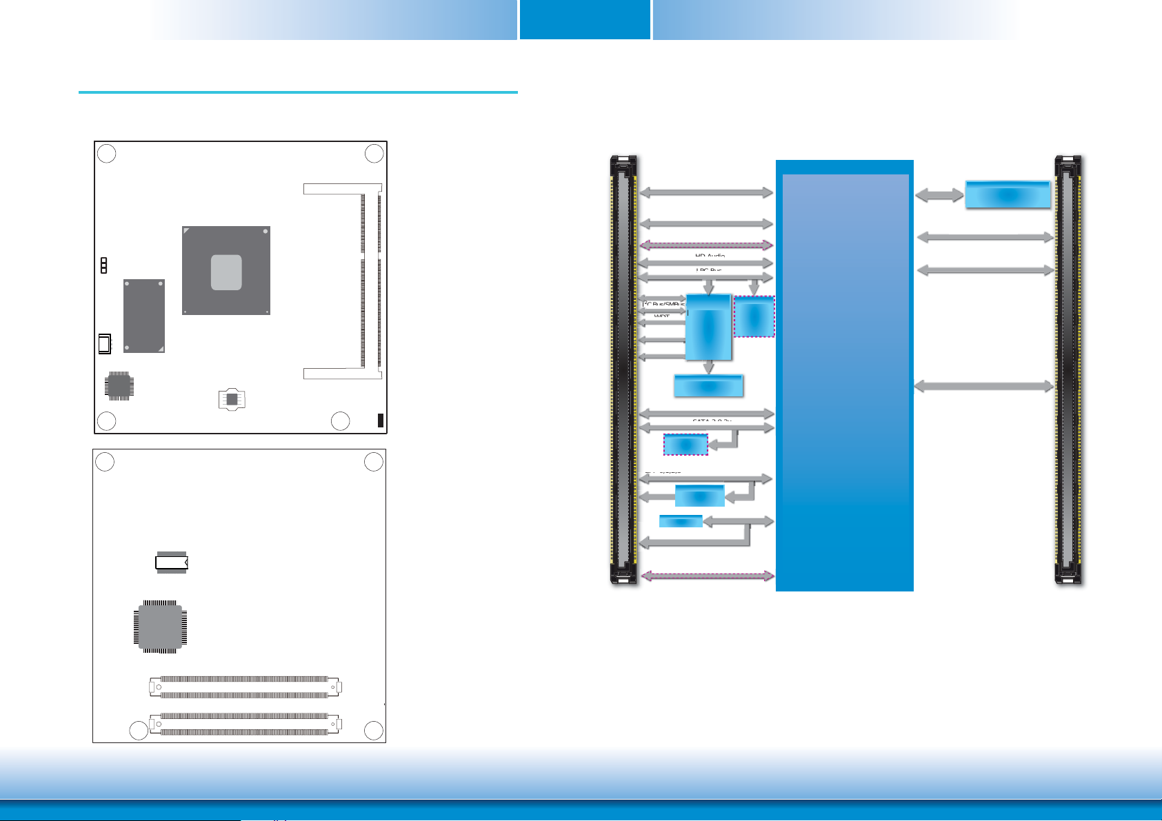
Chapter 3 - Hardware Installation
HD Audio
LPC Bus
USB 2.0 8x
SATA 3.0 2x
PCIe GEN2 (GFX 1 x4)
USB_SS 0,1
USB 3.0
8bit DIO
C Bus/SMBus
0,1,
2,3
G
SD Card I/F (Optional)
SMBus (Optional)
Board Layout
Power-on
Select (JP1)
1
1
CPU
Fan
SSD
(optional)
Intel
WGI210AT
AMD
G-Series SoC
SPI Flash
BIOS
DDR3 SODIMM
Standby
Power LED
Top View
Chapter 3
Block Diagram
LVDS Port
(Single Channel)
VGA
SMBus (Optional)
HD Audio
LPC Bus
8-bit DIO
2
I
A / B
C Bus/SMBus
WDT
Serial Port1,
2 Tx/Rx
Sys Fan
PWM/TACH
SSD Chip
(Optional)
GPP 0,1,2,3
LAN
SPI ROM
SPI Bus
Embedded
Controller
IT8518E
CMOS Backup
EEPROM
USB 2.0 8x
SATA 3.0 2x
LAN
TPM 1.2
SLB9635
(Optional)
SATA 1
PCIe GEN2
(1 x4 or 4 x1
LTDP0
LPC
GPP 3
SPI I/F
AMD Embedded
G-Series SoC
1066~1600MT/s
PCIe GEN2 (GFX 1 x4)
TDP1
UNBUFFERED
DDR3 SODIMM
DDI Port 1
USB_SS 0,1USB 3.0
C / D
ITE
IT8518E
D110
C110
B110
A110
TPM
(optional)
COM Express connector
COM Express connector
SD Card I/F (Optional)
Bottom View
D1
C1
B1
A1
10
www.dfi .comChapter 3 Hardware Installation
Page 11

Mechanical Diagram
Chapter 3
KB968 Module with Thermal Solution
53.00
Fan
95.00
Heat sink
95.00
91.00
87.00
0.00
4.00
KB968 Module
4.00
0.00
0.00
4.00
76.00
87.00
91.00
91.00
91.00
87.00
0.00
4.00
Top View
Heat spreader
53.00
11.00 22.00 20.00
Standoff
Module PCB
2.00
Side View of the Module with Thermal Solution and Carrier Board
Bottom View
14.00
2.00
0.00
0.00
70.20
11
12.50
www.dfi .comChapter 3 Hardware Installation
Page 12

Chapter 3
System Memory
Important:
Electrostatic discharge (ESD) can damage your board, processor, disk drives, add-in
boards, and other components. Perform installation procedures at an ESD workstation
only. If such a station is not available, you can provide some ESD protection by wearing an antistatic wrist strap and attaching it to a metal part of the system chassis. If
a wrist strap is unavailable, establish and maintain contact with the system chassis
throughout any procedures requiring ESD protection.
System Memory
The system board is equipped with one 204-pin SODIMM socket that supports DDR3
1066/1333/1600MHz
figure shown below.
Important:
When the Standby Power LED lit red, it indicates that there is power on the board.
Power-off the PC then unplug the power cord prior to installing any devices. Failure to
do so will cause severe damage to the board and components.
(-420C/-415G/-217G) or 1066/1333MHz (-210H) memory interface as the
Installing the DIMM Module
Note:
The system board used in the following illustrations may not resemble the actual one.
These illustrations are for reference only.
1. Make sure the PC and all other peripheral devices connected to it has been powered down.
2. Disconnect all power cords and cables.
3. Locate the SODIMM socket on the system board.
4. Note the key on the socket. The key ensures the module can be plugged into the socket in
only one direction.
Standby
Power LED
DDR3
12
www.dfi .comChapter 3 Hardware Installation
Page 13

Chapter 3
5. Grasping the module by its edges, align the module into the socket at an approximately 30
degrees angle. Apply firm even pressure to each end of the module until it slips down into
the socket. The contact fingers on the edge of the module will almost completely disappear
inside the socket.
6. Push down the module until the clips at each end of the socket lock into position. You will
hear a distinctive “click”, indicating the module is correctly locked into position.
Clip
Clip
13
www.dfi .comChapter 3 Hardware Installation
Page 14
Chapter 3
Connectors
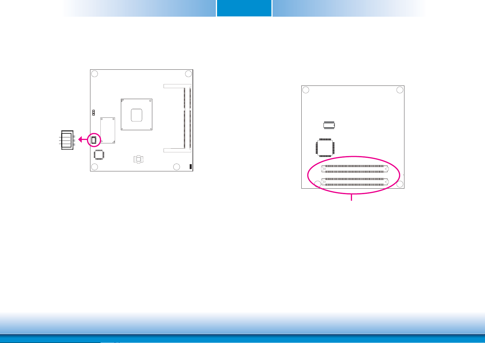
CPU Fan Connector
Sense
+12V
Ground
Connect the CPU fan’s cable connector to the CPU fan connector on the board. The cooling fan
will provide adequate airflow throughout the chassis to prevent overheating the CPU and board
components.
BIOS Setting
1
3
COM Express Connectors
The COM Express connectors are used to interface the KB968 COM Express board to a carrier
board. Connect the COM Express connectors (located on the solder side of the board) to the
COM Express connectors on the carrier board.
Refer to the “Installing KB968 onto a Carrier Board” section for more information.
COM Express Connectors
“PC Health Status” submenu in the Advanced menu of the BIOS will display the current speed
of the cooling fan. Refer to the chapter 4 of the manual for more information
.
Refer to the following pages for the pin functions of these connectors.
14
www.dfi .comChapter 3 Hardware Installation
Page 15

COM Express Connectors
A
)
)
A
A
A
A
A
A
A
A
A
)
)
A
A
A
A
A
A
A
A
A
A
A
)
)
A
A
A
A
A
A
F
A
A
A
)
)
A
A
A
A
A
A
A
A
A
A
A
)
)
A
A
A
A
A
A
A
A
A
)
)
A
A
A
A
A28(S)
A
K
L
A29AC/
C
A
Y
A30AC/
A
Y
A
)
)
A
Y
A32AC/
K
A
Y
A33AC/
T
K
A
A
T
A
A
A
)
)
A
A
R
A
A
A
A
A
A
A
A
K
A
)
)
A
T
A
A
A
A
X
A
A
X
A
A
)
)
A
A
X
A47V
C
A
X
A
A
A
A104
V
V
V
A
Q
A
V
V
A
)
)
A
V
V
A
A
V
V
A
A
V
V
A
A
V
V
A
A
)
)
A
A
)
(
)
)
(
)
X
)
)
(
)
D
(
)
)
-
-
(
)
+
X
(
)
)
X
-
(
)
-
D
D
(
)
)
-
4
V
V
4
V
V
-
V
V
)
V
V
/
V
V
V
V
V
V
)
)
Chapter 3
1 GND (FIXED
2 GBE0_MDI3- B2 GBE0_ACT#
3 GBE0_MDI3+ B3 LPC_FRAME#
4 GBE0_LINK100# B4 LPC_AD0
5 GBE0_LINK1000# B5 LPC_AD1
6 GBE0_MDI2- B6 LPC_AD2
7 GBE0_MDI2+ B7 LPC_AD3
8 GBE0_LINK# B8 LPC_DRQ0#
9 GBE0_MDI1- B9 LPC_DRQ1#
10 GBE0_MDI1+ B10 LPC_CLK
11 GND (FIXED
12 GBE0_MDI0- B12 PWRBTN#
13 GBE0_MDI0+ B13 SMB_CK
14 GBE0_CTRE
15 SUS_S3# B15 SMB_ALERT#
16 SATA0_TX+ B16 SATA1_TX+
17 SATA0_TX- B17 SATA1_TX18 SUS_S4# B18 SUS_STAT#
19 SATA0_RX+ B19 SATA1_RX+
20 SATA0_RX- B20 SATA1_RX21 GND (FIXED
22 SATA2_TX+ B22 SATA3_TX+
23 SATA2_TX- B23 SATA3_TX24 SUS_S5# B24 PWR_OK
25 SATA2_RX+ B25 SATA3_RX+
26 SATA2_RX- B26 SATA3_RX27 BATLOW# B27 WDT
31 GND (FIXED
34 BIOS_DIS0# B34 I2C_DA
35 THRMTRIP# B35 THRM#
36 USB6- B36 USB737 USB6+ B37 USB7+
38 USB_6_7_OC# B38 USB_4_5_OC#
39 USB4- B39 USB540 USB4+ B40 USB5+
41 GND (FIXED
42 USB2- B42 USB343 USB2+ B43 USB3+
44 USB_2_3_OC# B44 USB_0_1_OC#
45 USB0- B45 USB146 USB0+ B46 USB1+
48 EXCD0_PERST# B48 EXCD1_CPPE#
49 EXCD0_CPPE# B49 SYS_RESET#
50 LPC_SERIR
51 GND (FIXED
52 PCIE_TX5+ B52 PCIE_RX5+
53 PCIE_TX5- B53 PCIE_RX554 GPI0 B54 GPO1
55 PCIE_TX4+ B55 PCIE_RX4+
Row
ATA_ACT# B28AC_SDIN2
HDA_SYN
HDA _RST# B30AC_SDIN0
HDA _BITCL
HDA _SDOU
CC_RT
B1 GND (FIXED
B11 GND (FIXED
B14 SMB_DAT
B21 GND (FIXED
B29AC_SDIN1
B31 GND (FIXED
B32 SPKR
B33 I2C_C
B41 GND (FIXED
B47 EXCD1_PERST#
B50 CB_RESET#
B51 GND (FIXED
RowB Row
56 PCIE_TX4- B56 PCIE_RX457 GND B57 GPO2
58 PCIE_TX3+ B58 PCIE_RX3+
59 PCIE_TX3- B59 PCIE_RX360 GND (FIXED
61 PCIE_TX2+ B61 PCIE_RX2+
62 PCIE_TX2- B62 PCIE_RX263 GPI1 B63 GPO3
64 PCIE_TX1+ B64 PCIE_RX1+
65 PCIE_TX1- B65 PCIE_RX166 GND B66 WAKE0#
67 GPI2 B67 WAKE1#
68 PCIE_TX0+ B68 PCIE_RX0+
69 PCIE_TX0- B69 PCIE_RX070 GND (FIXED
71 LVDS_A0+ B71 LVDS_B0+
72 LVDS_A0- B72 LVDS_B073 LVDS_A1+ B73 LVDS_B1+
74 LVDS_A1- B74 LVDS_B175 LVDS_A2+ B75 LVDS_B2+
76 LVDS_A2- B76 LVDS_B277 LVDS_VDD_EN B77 LVDS_B3+
78 LVDS_A3+ B78 LVDS_B379 LVDS_A3- B79 LVDS_BKLT_EN
80 GND (FIXED
81 LVDS_A_CK+ B81 LVDS_B_CK+
82 LVDS_A_CK- B82 LVDS_B_CK83 LVDS_I2C_C
84 LVDS_I2C_DATB84VCC_5V_SB
85 GPI3 B85VCC_5V_SB
86 RSVD B86VCC_5V_SB
87 RSVD B87VCC_5V_SB
88 PCIE0_CK_REF+ B88 BIOS_DIS1#
89 PCIE0_CK_REF- B89VGA_RED
90 GND (FIXED
91 SPI_POWE
92 SPI_MISO B92VGA_BLU
93 GPO0 B93VGA_HSYNC
94 SPI_CLK B94VGA_VSYNC
95 SPI_MOSI B95VGA_I2C_C
96 TPM_PP B96VGA_I2C_DA
97 TYPE10# B97 SPI_CS#
98 SER0_T
99 SER0_R
100 GND (FIXED
101 SER1_T
102 SER1_R
103 LID# B103 SLEEP#
CC_12
105VCC_12
106VCC_12
107VCC_12
108VCC_12
109VCC_12
110 GND (FIXED
B60 GND (FIXED
B70 GND (FIXED
B80 GND (FIXED
B83 LVDS_BKLT_CTR
B90 GND (FIXED
B91VGA_GRN
B98 RSVD
B99 RSVD
B100 GND (FIXED
B101 FAN_PWMOUT
B102 FAN_TACHIN
B104VCC_12
B105VCC_12
B106VCC_12
B107VCC_12
B108VCC_12
B109VCC_12
B110 GND (FIXED
RowB
C1 GND (FIXED
C2 GND D2 GND C57 TYPE1# D57 TYPE2#
C3 USB_SSRX0- D3 USB_SSTX0- C58 PEG_RX2+ D58 PEG_TX2+
C4 USB_SSRX0+ D4 USB_SSTX0+ C59 PEG_RX2- D59 PEG_TX2C5 GND D5 GND C60 GND
C6 USB_SSRX1- D6 USB_SSTX1- C61 PEG_RX3+ D61 PEG_TX3+
C7 USB_SSRX1+ D7 USB_SSTX1+ C62 PEG_RX3- D62 PEG_TX3C8 GND D8 GND C63 RSVD D63 RSVD
C9 USB_SSRX2- D9 USB_SSTX2- C64 RSVD D64 RSVD
C10 USB_SSRX2+ D10 USB_SSTX2+ C65 PEG_RX4+ D65 PEG_TX4+
C11 GND
C12 USB_SSRX3- D12 USB_SSTX3- C67 NC D67 GND
C13 USB_SSRX3+ D13 USB_SSTX3+ C68 PEG_RX5+ D68 PEG_TX5+
C14 GND D14 GND C69 PEG_RX5- D69 PEG_TX5C15 NC D15 DDI1_CTRLCLK_AU
C16 NC D16 DDI1_CTRLDATA_AC71 PEG_RX6+ D71 PEG_TX6+
C17 RSVD D17 RSVD C72 PEG_RX6- D72 PEG_TX6C18 RSVD D18 RSVD C73 GND D73 GND
C19 PCIE_RX6+ D19 PCIE_TX6+ C74 PEG_RX7+ D74 PEG_TX7+
C20 PCIE_RX6- D20 PCIE_TX6- C75 PEG_RX7- D75 PEG_TX7C21 GND
C22 NC D22 NC C77 RSVD D77 RSVD
C23 NC D23 NC C78 PEG_RX8+ D78 PEG_TX8+
C24 DDI1_HP
C25 NC D25 RSVD C80 GND
C26 NC D26 DDI1_PAIR0+ C81 PEG_RX9+ D81 PEG_TX9+
C27 RSVD D27 DDI1_PAIR0
C28 RSVD D28 RSVD C83 RSVD D83 RSVD
C29 NC D29 DDI1_PAIR1+ C84 GND D84 GND
C30 NC D30 DDI1_PAIR1
C31 GND
C32 DDI2_CTRLCLK_AUX
C33 DDI2_CTRLDATA_AU
C34 RSVD D34 RSVD C89 PEG_RX11- D89 PEG_TX11C35 RSVD D35 RSVD C90 GND
C36 DDI3_CTRLCLK_AUX+D36 DDI1_PAIR3+ C91 PEG_RX12+ D91 PEG_TX12+
C37 DDI3_CTRLDATA_AU
C38 RSVD D38 RSVD C93 GND D93 GND
C39 DDI3_PAIR0+ D39 DDI2_PAIR0+ C94 PEG_RX13+ D94 PEG_TX13+
C40 DDI3_PAIR0
C41 GND
C42 DDI3_PAIR1+ D42 DDI2_PAIR1+ C97 RSVD D97 RSVD
C43 DDI3_PAIR1
C44 DDI3_HP
C45 RSVD D45 RSVD C100 GND
C46 DDI3_PAIR2+ D46 DDI2_PAIR2+ C101 PEG_RX15+ D101 PEG_TX15+
C47 DDI3_PAIR2
C48 RSVD D48 RSVD C103 GND D103 GND
C49 DDI3_PAIR3+ D49 DDI2_PAIR3+ C10
C50 DDI3_PAIR3
C51 GND (FIXED
C52 PEG_RX0+
C53 PEG_RX0- D53 PEG_TX0- C108VCC_12
C54 TYPE0# D54 PEG_LANE_RV# C109VCC_12
C55 PEG_RX1+ D55 PEG_TX1+ C110 GND (FIXED
FIXED
FIXED
FIXED
FIXED
D1 GND (FIXED)C56 PEG_RX1- D56 PEG_TX1-
D11 GND (FIXED)C66 PEG_RX4- D66 PEG_TX4-
C70 GND (FIXED
D21 GND (FIXED)C76 GND D76 GND
D24 RSVD C79 PEG_RX8- D79 PEG_TX8-
C82 PEG_RX9- D82 PEG_TX9-
D31 GND (FIXED)C86 PEG_RX10- D86 PEG_TX10D32 DDI1_PAIR2+ C87 GND D87 GND
D33 DDI1_PAIR2-C88 PEG_RX11+ D88 PEG_TX11+
D37 DDI1_PAIR3-C92 PEG_RX12- D92 PEG_TX12-
D40 DDI2_PAIR0-C95 PEG_RX13- D95 PEG_TX13D41 GND (FIXED)C96 GND D96 GND
D43 DDI2_PAIR1-C98 PEG_RX14+ D98 PEG_TX14+
D44 DDI2_HP
D47 DDI2_PAIR2-C102 PEG_RX15- D102 PEG_TX15-
D50 DDI2_PAIR3-C105VCC_12
D51 GND (FIXED)C106VCC_12
D52 PEG_TX0+ C107VCC_12
C85 PEG_RX10+ D85 PEG_TX10+
C99 PEG_RX14- D99 PEG_TX14-
RowC RowDRowC RowD
CC_12
FIXED
FIXED
FIXED
FIXED
D60 GND (FIXED
D70 GND (FIXED
D80 GND (FIXED
D90 GND (FIXED
D100 GND (FIXED
D10
CC_12
D105VCC_12
D106VCC_12
D107VCC_12
D108VCC_12
D109VCC_12
D110 GND (FIXED
15
www.dfi .comChapter 3 Hardware Installation
Page 16

Chapter 3
_
A
/
A
s
COM Express Connectors Signal Description
Pin Types
I Input to the Module
O Output from the Module
I/O Bi-directional input / output signal
OD Open drain output
C97/HDA Signals Descriptions
Signal Pin# Pin Type Pwr Rail /Tolerance KB968 Carrier Board Description
AC/HAD_RST# A30 O CMOS 3.3V Suspend/3.3V Connect to CODEC pin 11 RESET# Reset output to CODEC, active low.
AC/HDA_SYNC A29 O CMOS 3.3V/3.3V Connect to CODEC pin 10 SYNC Sample-synchronization signal to the CODEC(s).
AC/HDA_BITCLK A32 I/O CMOS 3.3V/3.3V Connect to CODEC pin 6 BIT_CLK Serial data clock generated by the external CODEC(s).
AC/HDA_SDOUT A33 O CMOS 3.3V/3.3V Connect to CODEC pin 5 SDATA_OUT Serial TDM data output to the CODEC.
AC/HDA_SDIN2 B28 I/O CMOS 3.3V Suspend/3.3V Connect 33 ƻ in series to CODEC2 pin 8 SDATA_IN
AC/HDA_SDIN1 B29 I/O CMOS 3.3V Suspend/3.3V Connect 33 ƻ in series to CODEC1 pin 8 SDATA_IN
AC/HDA_SDIN0 B30 I/O CMOS 3.3V Suspend/3.3V Connect 33 ƻ in series to CODEC0 pin 8 SDATA_IN
Gigabit Ethernet Signals Description
Signal Pin# Pin Type Pwr Rail /Tolerance KB968 Carrier Board Description
GBE0_MDI0+ A13 I/O Analog 3.3V max Suspend
GBE0_MDI0- A12 I/O Analog 3.3V max Suspend
GBE0_MDI1+ A10 I/O Analog 3.3V max Suspend
GBE0_MDI1- A9 I/O Analog 3.3V max Suspend
GBE0_MDI2+ A7 I/O Analog 3.3V max Suspend
GBE0_MDI2- A6 I/O Analog 3.3V max Suspend
GBE0_MDI3+ A3 I/O Analog 3.3V max Suspend
GBE0
MDI3GBE0_ACT# B2 OD CMOS 3.3V Suspend/3.3V
GBE0_LINK# A8 OD CMOS 3.3V Suspend/3.3V NA Gigabit Ethernet Controller 0 link indicator, active low.
GBE0_LINK100# A4 OD CMOS 3.3V Suspend/3.3V
GBE0_LINK1000# A5 OD CMOS 3.3V Suspend/3.3V
SATA Signals Descriptions
Signal Pin# Pin Type Pwr Rail /Tolerance KB968 Carrier Board Description
SATA0_TX+ A16 O SATA AC coupled on Module AC Coupling capacitor
SATA0_TX- A17 O SATA AC coupled on Module AC Coupling capacitor
SATA0_RX+ A19 I SATA AC coupled on Module AC Coupling capacitor
SATA0_RX- A20 I SATA AC coupled on Module AC Coupling capacitor
SATA1_TX+ B16 O SATA AC coupled on Module AC Coupling capacitor
SATA1_TX- B17 O SATA AC coupled on Module AC Coupling capacitor
SATA1_RX+ B19 I SATA AC coupled on Module AC Coupling capacitor
SATA1_RX- B20 I SATA AC coupled on Module AC Coupling capacitor
SATA2_TX+ A22 O SATA AC coupled on Module NA
SATA2_TX- A23 O SATA AC coupled on Module NA
SATA2_RX+ A25 I SATA AC coupled on Module NA
SATA2_RX- A26 I SATA AC coupled on Module NA
SATA3_TX+ B22 O SATA AC coupled on Module NA
SATA3_TX- B23 O SATA AC coupled on Module NA
SATA3_RX+ B25 I SATA AC coupled on Module NA
SATA3_RX- B26 I SATA AC coupled on Module NA
ATA_ACT# A28 I/O CMOS 3.3V / 3.3V
2I
O Analog3.3V max Suspend
Connect to Magnetics Module MDI0+/-
Connect to Magnetics Module MDI1+/-
Connect to Magnetics Module MDI2+/-
Connect to Magnetics Module MDI3+/Connect to LED and recommend current limit
resistor 150ȟ to 3.3VSB
Connect to LED and recommend current limit
resistor 150ȟ to 3.3VSB
Connect to LED and recommend current limit
resistor 150ȟ to 3.3VSB
Connect to SATA0 Conn TX pin
Connect to SATA0 Conn RX pin
Connect to SATA1 Conn TX pin
Connect to SATA1 Conn RX pin
NA
NA
NA
NA
Connect to LED and recommend current limit
resistor 220ƻ to 3.3V
Serial TDM data inputs from up to 3 CODECs.
Gigabit Ethernet Controller 0: Media Dependent Interface Differential
Pairs 0,1,2,3. The MDI can operate in 1000, 100 and 10 Mbit / sec
modes. Some pairs are unused in some modes, per the following:
1000BASE-T 100BASE-TX 10BASE-T
MDI[0]+/- B1_DA+/- TX+/- TX+/ MDI[1]+/- B1_DB+/- RX+/- RX+/ MDI[2]+/- B1_DC+/ MDI[3]+/- B1_DD+/-
Gigabit Ethernet Controller 0 activity indicator, active low.
Gigabit Ethernet Controller 0 1000 Mbit / sec link indicator, active low.
Gigabit Ethernet Controller 0 1000 Mbit / sec link indicator, active low.
Serial ATA or SAS Channel 0 transmit differential pair.
Serial ATA or SAS Channel 0 receive differential pair.
Serial ATA or SAS Channel 1 transmit differential pair.
Serial ATA or SAS Channel 1 receive differential pair.
Serial ATA or SAS Channel 2 transmit differential pair.
Serial ATA or SAS Channel 2 receive differential pair.
Serial ATA or SAS Channel 3 transmit differential pair.
Serial ATA or SAS Channel 3 receive differential pair.
ATA (parallel and serial) or SAS activity indicator, active low.
16
www.dfi .comChapter 3 Hardware Installation
Page 17

Chapter 3
PCI Express Lanes Signals Descriptions
Signal Pin# Pin Type Pwr Rail /Tolerance KB968 Carrier Board Description
PCIE_TX0+ A68 AC Coupling capacitor
PCIE_TX0- A69 AC Coupling capacitor
PCIE_RX0+ B68
PCIE_RX0- B69
PCIE_TX1+ A64 AC Coupling capacitor
PCIE_TX1- A65 AC Coupling capacitor
PCIE_RX1+ B64
PCIE_RX1- B65
PCIE_TX2+ A61 AC Coupling capacitor
PCIE_TX2- A62 AC Coupling capacitor
PCIE_RX2+ B61
PCIE_RX2- B62
PCIE_TX3+ A58 NA
PCIE_TX3- A59 NA
PCIE_RX3+ B58 NA
PCIE_RX3- B59 NA
PCIE_TX4+ A55 NA
PCIE_TX4- A56 NA
PCIE_RX4+ B55 NA
PCIE_RX4- B56 NA
PCIE_TX5+ A52 NA
PCIE_TX5- A53 NA
PCIE_RX5+ B52 NA
PCIE_RX5- B53 NA
PCIE_TX6+ D19 NA
PCIE_TX6- D20 NA
PCIE_RX6+ C19 NA
PCIE_RX6- C20 NA
PCIE_TX7+ D22 NA
PCIE_TX7- D23 NA
PCIE_RX7+ C22 NA
PCIE_RX7- C23 NA
PCIE0_CK_REF+ A88
PCIE0_CK_REF- A89
PEG Signals Descriptions
Signal Pin# Pin Type Pwr Rail /Tolerance KB968 Carrier Board Description
PEG_TX0+ D52 AC Coupling capacitor
PEG_TX0- D53 AC Coupling capacitor
PEG_RX0+ C52
PEG_RX0- C53
PEG_TX1+ D55 AC Coupling capacitor
PEG_TX1- D56 AC Coupling capacitor
PEG_RX1+ C55
PEG_RX1- C56
PEG_TX2+ D58 AC Coupling capacitor
PEG_TX2- D59 AC Coupling capacitor
PEG_RX2+ C58
PEG_RX2- C59
PEG_TX3+ D61 AC Coupling capacitor
PEG_TX3- D62 AC Coupling capacitor
PEG_RX3+ C61
PEG_RX3- C62
PEG_TX4+ D65 NA
PEG_TX4- D66 NA
PEG_RX4+ C65 NA
PEG_RX4- C66 NA
PEG_TX5+ D68 NA
PEG_TX5- D69 NA
PEG_RX5+ C68 NA
PEG_RX5- C69 NA
O PCIE AC coupled on Module PCI Express Differential Transmit Pairs 0
I PCIE AC coupled off Module PCI Express Differential Receive Pairs 0
O PCIE AC coupled on Module PCI Express Differential Transmit Pairs 1
I PCIE AC coupled off Module
O PCIE AC coupled on Module PCI Express Differential Transmit Pairs 2
I PCIE AC coupled off Module PCI Express Differential Receive Pairs 2
O PCIE AC coupled on Module NA
I PCIE AC coupled off Module
O PCIE AC coupled on Module
I PCIE AC coupled off Module
O PCIE AC coupled on Module PCI Express Differential Transmit Pairs 5
I PCIE AC coupled off Module PCI Express Differential Receive Pairs 5
O PCIE AC coupled on Module PCI Express Differential Transmit Pairs 6
I PCIE AC coupled off Module
O PCIE AC coupled on Module PCI Express Differential Transmit Pairs 7
I PCIE AC coupled off Module
O PCIE PCIE
O PCIE AC coupled on Module PCI Express Graphics transmit differential pairs 0
I PCIE AC coupled off Module PCI Express Graphics receive differential pairs 0
O PCIE AC coupled on Module PCI Express Graphics transmit differential pairs 1
I PCIE
I PCIE AC coupled off Module PCI Express Graphics receive differential pairs 2
O PCIE AC coupled on Module PCI Express Graphics transmit differential pairs 3
I PCIE AC coupled off Module PCI Express Graphics receive differential pairs 3
O PCIE AC coupled on Module
I PCIE AC coupled off Module
I PCIE AC coupled off Module PCI Express Graphics receive differential pairs 5NA
AC coupled off Module PCI Express Graphics receive differential pairs 1
Connect to PCIE device or slot
Device - Connect AC Coupling cap 0.1uF
Slot - Connect to PCIE Conn pin
Connect to PCIE device or slot
Device - Connect AC Coupling cap 0.1uF
Slot - Connect to PCIE Conn pin
Connect to PCIE device or slot
Device - Connect AC Coupling cap 0.1uF
Slot - Connect to PCIE Conn pin
NA
NA
NA
NA
NA
NA
NA
NA
NA
Connect to PCIE device, PCIe CLK Buffer or slot
Connect to PCIE device or slot
Connect AC Coupling cap 0.1uF
Connect to PCIE device or slot
Connect AC Coupling cap 0.1uF
Connect to PCIE device or slotO PCIE AC coupled on Module
Connect AC Coupling cap 0.1uF
Connect to PCIE device or slot
Connect AC Coupling cap 0.1uF
NA
NA
PCI Express Differential Receive Pairs 1
PCI Express Differential Transmit Pairs 3
(Optional with on board LAN, Default setting as NC)
PCI Express Differential Receive Pairs 3
(Optional with on board LAN, Default setting as NC)
PCI Express Differential Transmit Pairs 4
PCI Express Differential Receive Pairs 4
PCI Express Differential Receive Pairs 6
PCI Express Differential Receive Pairs 7
Reference clock output for all PCI Express and PCI Express Graphics
lanes.
PCI Express Graphics transmit differential pairs 2
PCI Express Graphics transmit differential pairs 4
PCI Express Graphics receive differential pairs 4
PCI Express Graphics transmit differential pairs 5NAO PCIE AC coupled on Module
17
www.dfi .comChapter 3 Hardware Installation
Page 18

Chapter 3
PEG Signals Descriptions
Signal Pin# Pin Type Pwr Rail /Tolerance KB968 Carrier Board Description
PEG_TX6+ D71 NA
PEG_TX6- D72 NA
PEG_RX6+ C71 NA
PEG_RX6- C72 NA
PEG_TX7+ D74 NA
PEG_TX7- D75 NA
PEG_RX7+ C74 NA
PEG_RX7- C75 NA
PEG_TX8+ D78 NA
PEG_TX8- D79 NA
PEG_RX8+ C78 NA
PEG_RX8- C79 NA
PEG_TX9+ D81 NA
PEG_TX9- D82 NA
PEG_RX9+ C81 NA
PEG_RX9- C82 NA
PEG_TX10+ D85 NA
PEG_TX10- D86 NA
PEG_RX10+ C85 NA
PEG_RX10- C86 NA
PEG_TX11+ D88 NA
PEG_TX11- D89 NA
PEG_RX11+ C88 NA
PEG_RX11- C89 NA
PEG_TX12+ D91 NA
PEG_TX12- D92 NA
PEG_RX12+ C91 NA
PEG_RX12- C92 NA
PEG_TX13+ D94 NA
PEG_TX13- D95 NA
PEG_RX13+ C94 NA
PEG_RX13- C95 NA
PEG_TX14+ D98 NA
PEG_TX14- D99 NA
PEG_RX14+ C98 NA
PEG_RX14- C99 NA
PEG_TX15+ D101 NA
PEG_TX15- D102 NA
PEG_RX15+ C101 NA
PEG_RX15- C102 NA
PEG_LANE_RV# D54 I CMOS 3.3V / 3.3V
ExpressCard Signals Descriptions
Signal Pin# Pin Type Pwr Rail /Tolerance KB968 Carrier Board Description
EXCD0_CPPE# A49 PU 40-50k to 3.3V
EXCD1_CPPE# B48 PU 40-50k to 3.3V
EXCD0_PERST# A48
EXCD1_PERST# B47
O PCIE AC coupled on Module PCI Express Graphics transmit differential pairs 6NA
I PCIE AC coupled off Module PCI Express Graphics receive differential pairs 6
O PCIE
I PCIE AC coupled off Module PCI Express Graphics receive differential pairs 7
I PCIE AC coupled off Module
O PCIE AC coupled on Module PCI Express Graphics transmit differential pairs 9
I PCIE AC coupled off Module PCI Express Graphics receive differential pairs 9
O PCIE AC coupled on Module PCI Express Graphics transmit differential pairs 10
I PCIE AC coupled off Module
O PCIE AC coupled on Module PCI Express Graphics transmit differential pairs 11
I PCIE AC coupled off Module PCI Express Graphics receive differential pairs 11
O PCIE AC coupled on Module
I PCIE AC coupled off Module
O PCIE AC coupled on Module PCI Express Graphics transmit differential pairs 13
I PCIE AC coupled off Module
O PCIE AC coupled on Module PCI Express Graphics transmit differential pairs 14
I PCIE AC coupled off Module
O PCIE AC coupled on Module PCI Express Graphics transmit differential pairs 15
I PCIE AC coupled off Module PCI Express Graphics receive differential pairs 15
I CMOS 3.3V /3.3V
O CMOS 3.3V /3.3V PCI ExpressCard: reset, active low, one per card
AC coupled on Module PCI Express Graphics transmit differential pairs 7
NA
NA
NA
NAO PCIE AC coupled on Module
NA
NA
NA
NA
NA
NA
NA
NA
NA
NA
NA
NA
NA
NA
PCI Express Graphics transmit differential pairs 8
PCI Express Graphics receive differential pairs 8
PCI Express Graphics receive differential pairs 10NA
PCI Express Graphics transmit differential pairs 12
PCI Express Graphics receive differential pairs 12
PCI Express Graphics receive differential pairs 13
PCI Express Graphics receive differential pairs 14
PCI Express Graphics lane reversal input strap. Pull low on the Carrier
board to reverse lane order.
PCI ExpressCard: PCI Express capable card request, active low, one per
card
18
www.dfi .comChapter 3 Hardware Installation
Page 19

Chapter 3
/
DDI Signals Descriptions
Signal Pin# Pin Type Pwr Rail /Tolerance KB968 Carrier Board Description
DDI1_PAIR0+/SDVO1_RED+ D26 Connect AC Coupling Capacitors 0.1uF to Device
DDI1_PAIR0DDI1_PAIR1+/SDVO1_GRN+ D29 Connect AC Coupling Capacitors 0.1uF to Device
DDI1_PAIR1-/SDVO1_GRN- D30 Connect AC Coupling Capacitors 0.1uF to Device
DDI1_PAIR2+/SDVO1_BLU+ D32 Connect AC Coupling Capacitors 0.1uF to Device
DDI1_PAIR2-/SDVO1_BLU- D33 Connect AC Coupling Capacitors 0.1uF to Device
DDI1_PAIR3+/SDVO1_CK+ D36 Connect AC Coupling Capacitors 0.1uF to Device
DDI1_PAIR3-/SDVO1_CK- D37 Connect AC Coupling Capacitors 0.1uF to Device
DDI1_PAIR4+/SDVO1_INT+ C25 NA NA
DDI1_PAIR4-/SDVO1_INT- C26 NA NA
DDI1_PAIR5+/SDVO1_TVCLKIN+ C29 NA NA
DDI1_PAIR5-/SDVO1_TVCLKIN- C30 NA NA
DDI1_PAIR6+/SDVO1_FLDSTALL+ C15 NA NA
DDI1_PAIR6-/SDVO1_FLDSTALL- C16 NA NA
DDI1_CTRLCLK_AUX+/SDVO1_CTRLCLK D15
DDI1_CTRLCLK_AUX/SDVO1_CTRLDATA
SDVO1_RED- D27 Connect AC Coupling Capacitors 0.1uF to Device
D16
O PCIE AC coupled off Module
O PCIE AC coupled off Module DDI 1 Pair 1 differential pairs/Serial Digital Video B green output differential pair
O PCIE
O PCIE AC coupled off Module DDI 1 Pair 3 differential pairs/Serial Digital Video B clock output differential pair.
I PCIE
I PCIE AC coupled off Module Serial Digital Video TVOUT synchronization clock input differential pair.
I PCIE
I/O PCIE AC coupled on Module PD 100K to GND Connect to DP AUX+ DP AUX+ function if DDI1_DDC_AUX_SEL is no connect
I/O OD CMOS 3.3V / 3.3V NA NA
I/O PCIE AC coupled on Module PU 100K to 3.3V Connect to DP AUX- DP AUX- function if DDI1_DDC_AUX_SEL is no connect
I/O OD CMOS 3.3V / 3.3V NA NA
AC coupled off Module DDI 1 Pair 2 differential pairs/Serial Digital Video B blue output differential pair
AC coupled off Module
AC coupled off Module Serial Digital Video Field Stall input differential pair.
DDI 1 Pair 0 differential pairs/Serial Digital Video B red output differential pair
Serial Digital Video B interrupt input differential pair.
HDMI/DVI I2C CTRLCLK if DDI1_DDC_AUX_SEL is pulled high
(Optional with Displayport 1, Default setting as NC)
HDMI/DVI I2C CTRLDATA if DDI1_DDC_AUX_SEL is pulled high
(Optional with Displayport 1, Default setting as NC)
DDI1_HPD C24 I CMOS 3.3V / 3.3V PD 1M and Connect to device Hot Plug Detect DDI Hot-Plug Detect
DDI1_DDC_AUX_SEL D34 I CMOS 3.3V / 3.3V NA NA
DDI2_PAIR0+ D39 NA NA
DDI2_PAIR0- D40 NA NA
DDI2_PAIR1+ D42 NA NA
DDI2_PAIR1- D43 NA NA
DDI2_PAIR2+ D46 NA NA
DDI2_PAIR2- D47 NA NA
DDI2_PAIR3+ D49 NA NA
DDI2_PAIR3- D50 NA NA
DDI2_CTRLCLK_AUX+ C32
O PCIE AC coupled off Module
O PCIE AC coupled off Module
O PCIE AC coupled off Module
O PCIE AC coupled off Module
I/O PCIE AC coupled on Module NA NA
I/O OD CMOS 3.3V / 3.3V NA NA
19
Selects the function of DDI1_CTRLCLK_AUX+ and DDI1_CTRLDATA_AUX-.
DDI[n]_DDC_AUX_SEL shall be pulled to 3.3V on the Carrier with a 100K Ohm
resistor to configure the DDI[n]_AUX pair as the DDC channel.
Carrier DDI[n]_DDC_AUX_SEL should be connected to pin 13 of the DisplayPort
(Default setting as NC)
DDI 2 Pair 0 differential pairs
(Optional with LVDS, Default setting as NC)
DDI 2 Pair 1 differential pairs
(Optional with LVDS, Default setting as NC)
DDI 2 Pair 2 differential pairs
(Optional with LVDS, Default setting as NC)
DDI 2 Pair 3 differential pairs
(Optional with LVDS, Default setting as NC)
DP AUX+ function if DDI2_DDC_AUX_SEL is no connect
(Optional with LVDS, Default setting as NC)
HDMI/DVI I2C CTRLCLK if DDI2_DDC_AUX_SEL is pulled high
(Optional with LVDS, Default setting as NC)
www.dfi .comChapter 3 Hardware Installation
Page 20

Chapter 3
DDI Signals Descriptions
Signal Pin# Pin Type Pwr Rail /Tolerance KB968 Carrier Board Description
DP AUX- function if DDI2_DDC_AUX_SEL is no connect
(Optional with LVDS, Default setting as NC)
HDMI/DVI I2C CTRLDATA if DDI2_DDC_AUX_SEL is pulled high
(Optional with LVDS, Default setting as NC)
DDI2_CTRLCLK_AUX-
I/O PCIE AC coupled on Module NA NA
C33
I/O OD CMOS 3.3V / 3.3V NA NA
DDI2_HPD D44 I CMOS 3.3V / 3.3V NA NA
DDI2_DDC_AUX_SEL C34 I CMOS 3.3V / 3.3V NA NA
DDI3_PAIR0+ C39 NA NA
DDI3_PAIR0- C40 NA NA
DDI3_PAIR1+ C42 NA NA
DDI3_PAIR1- C43 NA NA
DDI3_PAIR2+ C46 NA NA
DDI3_PAIR2- C47 NA NA
DDI3_PAIR3+ C49 NA NA
DDI3_PAIR3- C50 NA NA
DDI3_CTRLCLK_AUX+ C36
DDI3_CTRLCLK_AUX- C37
DDI3_HPD C44 I CMOS 3.3V / 3.3V NA NA DDI Hot-Plug Detect
DDI3_DDC_AUX_SEL C38 I CMOS 3.3V / 3.3V NA NA
O PCIE AC coupled off Module
O PCIE DDI 3 Pair 1 differential pairs
O PCIE AC coupled off Module
O PCIE AC coupled off Module DDI 3 Pair 3 differential pairs
I/O PCIE AC coupled on Module NA NA DP AUX+ function if DDI3_DDC_AUX_SEL is no connect
I/O OD CMOS 3.3V / 3.3V NA NA HDMI/DVI I2C CTRLCLK if DDI3_DDC_AUX_SEL is pulled high
I/O PCIE AC coupled on Module NA NA DP AUX- function if DDI3_DDC_AUX_SEL is no connect
I/O OD CMOS 3.3V / 3.3V NA NA HDMI/DVI I2C CTRLDATA if DDI3_DDC_AUX_SEL is pulled high
AC coupled off Module
DDI Hot-Plug Detect
(Optional with LVDS, Default setting as NC)
Selects the function of DDI2_CTRLCLK_AUX+ and DDI2_CTRLDATA_AUX-.
DDI[n]_DDC_AUX_SEL shall be pulled to 3.3V on the Carrier with a 100K Ohm
resistor to configure the DDI[n]_AUX pair as the DDC channel.
Carrier DDI[n]_DDC_AUX_SEL should be connected to pin 13 of the DisplayPort
(Default setting as NC)
DDI 3 Pair 0 differential pairs
DDI 3 Pair 2 differential pairs
Selects the function of DDI3_CTRLCLK_AUX+ and DDI3_CTRLDATA_AUX-.
DDI[n]_DDC_AUX_SEL shall be pulled to 3.3V on the Carrier with a 100K Ohm
resistor to configure the DDI[n]_AUX pair as the DDC channel.
Carrier DDI[n]_DDC_AUX_SEL should be connected to pin 13 of the DisplayPort
20
www.dfi .comChapter 3 Hardware Installation
Page 21
Chapter 3
p
p
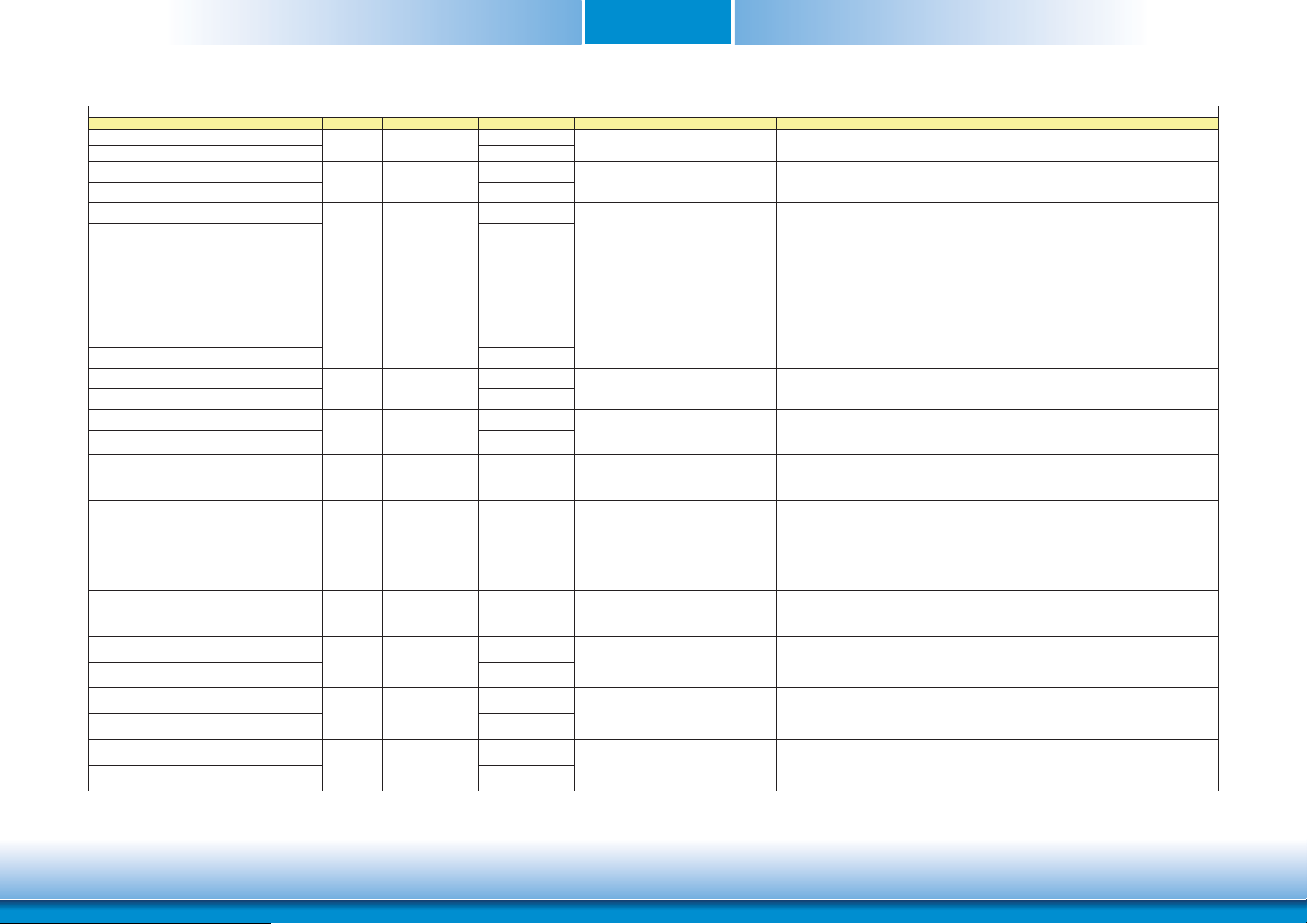
USB Signals Descriptions
Signal Pin# Pin Type Pwr Rail /Tolerance KB968 Carrier Board Description
USB0+ A46
USB0- A45
USB1+ B46
USB1- B45
USB2+ A43
USB2- A42
USB3+ B43
USB3- B42
USB4+ A40
USB4- A39
USB5+ B40
USB5- B39
USB6+ A37
USB6- A36
USB7+ B37
USB7- B36
USB_0_1_OC# B44 I CMOS 3.3V Suspend/3.3V PU 40-50k to 3.3VSB Connect to Overcurrent of USB Power Switch
USB_2_3_OC# A44 I CMOS 3.3V Suspend/3.3V PU 40-50k to 3.3VSB Connect to Overcurrent of USB Power Switch
USB_4_5_OC# B38 I CMOS 3.3V Suspend/3.3V PU 40-50k to 3.3VSB Connect to Overcurrent of USB Power Switch
USB_6_7_OC# A38 I CMOS 3.3V Suspend/3.3V PU 40-50k to 3.3VSB Connect to Overcurrent of USB Power Switch
USB_SSTX0+ D4 AC Coupling capacitor
USB_SSTX0- D3 AC Coupling capacitor
USB_SSRX0+ C4
USB_SSRX0- C3
USB_SSTX1+ D7 AC Coupling capacitor
USB_SSTX1- D6 AC Coupling capacitor
I/O USB 3.3V Suspend/3.3V USB differential pairs 0
I/O USB 3.3V Suspend/3.3V USB differential pairs 1
I/O USB 3.3V Suspend/3.3V USB differential pairs 2
I/O USB 3.3V Suspend/3.3V USB differential pairs 3
I/O USB
I/O USB 3.3V Suspend/3.3V USB differential pairs 5
I/O USB 3.3V Suspend/3.3V USB differential pairs 6
I/O USB 3.3V Suspend/3.3V
O PCIE AC coupled on Module Additional transmit signal differential pairs for the SuperSpeed USB data path.
I PCIE AC coupled off Module
O PCIE AC coupled on Module
3.3V Suspend/3.3V USB differential pairs 4
Connect 90ಳ @100MHz Common Choke in series
and ESD suppressors to GND to USB connector
Connect 90ಳ @100MHz Common Choke in series
and ESD suppressors to GND to USB connector
Connect 90ಳ @100MHz Common Choke in series
and ESD suppressors to GND to USB connector
Connect 90ಳ @100MHz Common Choke in series
and ESD suppressors to GND to USB connector
Connect 90ಳ @100MHz Common Choke in series
and ESD suppressors to GND to USB connector
Connect 90ಳ @100MHz Common Choke in series
and ESD suppressors to GND to USB connector
Connect 90ಳ @100MHz Common Choke in series
and ESD suppressors to GND to USB connector
Connect 90ಳ @100MHz Common Choke in series
and ESD suppressors to GND to USB connector
Connect 90ಳ @100MHz Common Choke in series
and ESD suppressors to GND to USB connector
Connect 90ಳ @100MHz Common Choke in series
and ESD suppressors to GND to USB connector
Connect 90ಳ @100MHz Common Choke in series
and ESD suppressors to GND to USB connector
USB differential pairs 7, USB7 may be configured as a USB client or as a host, or both, at the
Module designer's discretion.(KB968 default set as a host)
USB over-current sense, USB channels 0 and 1. A pull-up for this line
shall be present on the Module. An open drain driver from a USB
current monitor on the Carrier Board may drive this line low. Do not
pull this line high on the Carrier Board.
USB over-current sense, USB channels 2 and 3. A
shall be present on the Module. An open drain driver from a USB
current monitor on the Carrier Board may drive this line low. Do not
ull this line high on the Carrier Board.
USB over-current sense, USB channels 4 and 5. A pull-up for this line
shall be present on the Module. An open drain driver from a USB
current monitor on the Carrier Board may drive this line low. Do not
pull this line high on the Carrier Board.
USB over-current sense, USB channels 6 and 7. A pull-up for this line
shall be present on the Module. An open drain driver from a USB
current monitor on the Carrier Board may drive this line low. Do not
pull this line high on the Carrier Board.
Additional receive signal differential pairs for the SuperSpeed USB data path.
Additional transmit signal differential pairs for the SuperSpeed USB data path.
ull-up for this line
21
www.dfi .comChapter 3 Hardware Installation
Page 22
Chapter 3
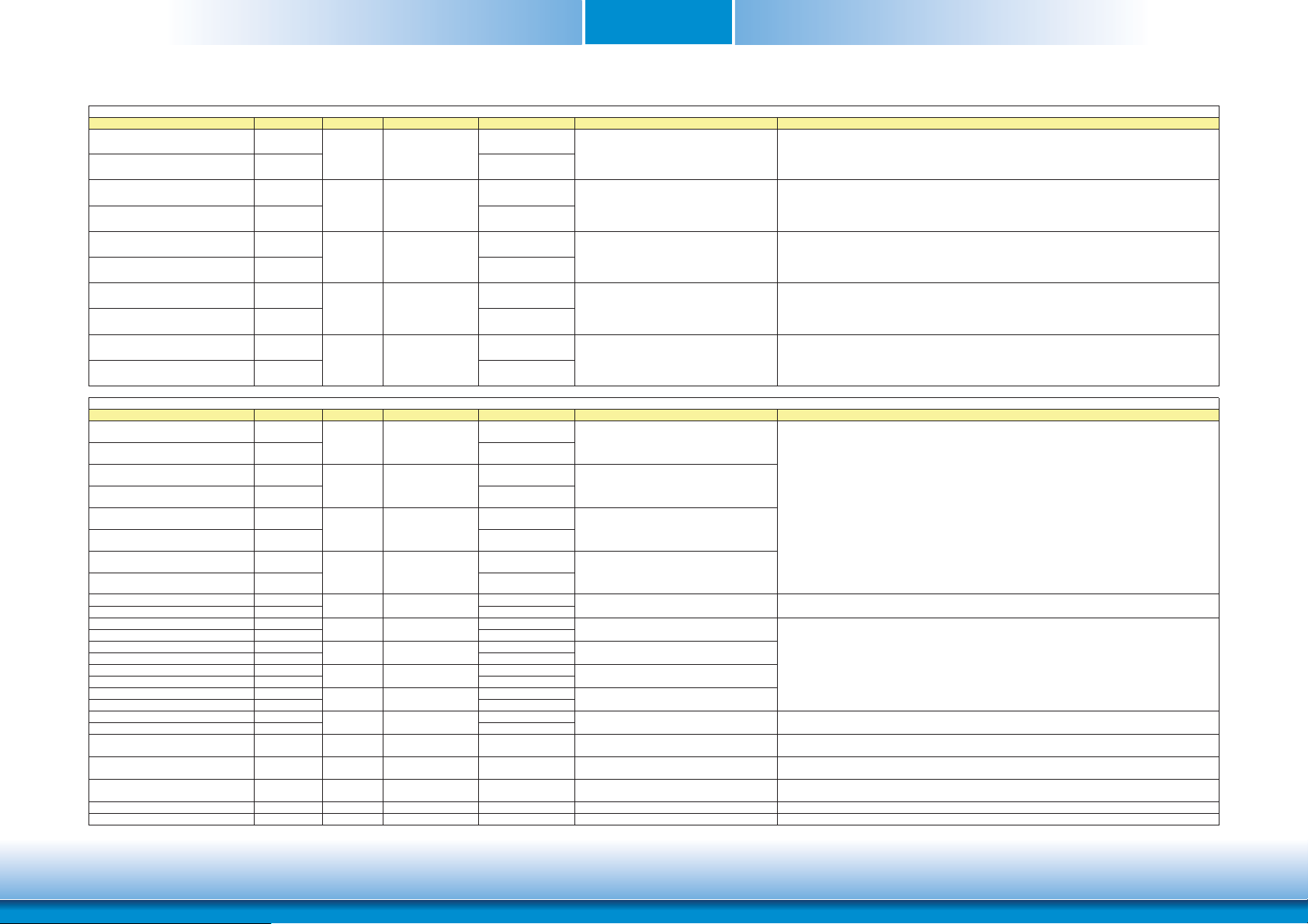
USB Signals Descriptions
Signal Pin# Pin Type Pwr Rail /Tolerance KB968 Carrier Board Description
USB_SSRX1+ C7
USB_SSRX1- C6
USB_SSTX2+ D10 NA
USB_SSTX2- D9 NA
USB_SSRX2+ C10 NA
USB_SSRX2- C9 NA
USB_SSTX3+ D13 NA
USB_SSTX3- D12 NA
USB_SSRX3+ C13 NA
USB_SSRX3- C12 NA
LVDS Signals Descriptions
Signal Pin# Pin Type Pwr Rail /Tolerance KB968 Carrier Board Description
LVDS_A0+ A71
LVDS_A0- A72
LVDS_A1+ A73
LVDS_A1- A74
LVDS_A2+ A75
LVDS_A2- A76
LVDS_A3+ A78 NA
LVDS_A3- A79 NA
LVDS_A_CK+ A81
LVDS_A_CK- A82
LVDS_B0+ B71 NA
LVDS_B0- B72 NA
LVDS_B1+ B73 NA
LVDS_B1- B74 NA
LVDS_B2+ B75 NA
LVDS_B2- B76 NA
LVDS_B3+ B77 NA
LVDS_B3- B78 NA
LVDS_B_CK+ B81 NA
LVDS_B_CK- B82 NA
LVDS_VDD_EN A77 O CMOS 3.3V / 3.3V
LVDS_BKLT_EN B79 O CMOS 3.3V / 3.3V
LVDS_BKLT_CTRL B83 O CMOS 3.3V / 3.3V
LVDS_I2C_CK A83 I/O OD CMOS 3.3V / 3.3V PU 4.7K to 3.3V Connect to DDC clock of LVDS panel I2C clock output for LVDS display use
LVDS_I2C_DAT A84 I/O OD CMOS 3.3V / 3.3V PU 4.7K to 3.3V Connect to DDC data of LVDS panel I2C data line for LVDS display use
I PCIE AC coupled off Module Additional receive signal differential pairs for the SuperSpeed USB data path.
O PCIE AC coupled on Module Additional transmit signal differential pairs for the SuperSpeed USB data path.
I PCIE AC coupled off Module Additional receive signal differential pairs for the SuperSpeed USB data path.
O PCIE
I PCIE AC coupled off Module Additional receive signal differential pairs for the SuperSpeed USB data path.
O LVDS LVDS Connect to LVDS connector
O LVDS Connect to LVDS connector
O LVDS LVDS
O LVDS LVDS
O LVDS LVDS
O LVDS
O LVDS
O LVDS LVDS NA
O LVDS LVDS NA
AC coupled on Module Additional transmit signal differential pairs for the SuperSpeed USB data path.
LVDS
LVDS
LVDS
Connect 90ಳ @100MHz Common Choke in series
and ESD suppressors to GND to USB connector
NA
NA
NA
NA
Connect to LVDS connector
NA
NA
NA
NA
Connect to enable control of LVDS panel power
Connect to enable control of LVDS panel backlight
Connect to brightness control of LVDS panel
circuit
power circuit.
backlight power circuit.
LVDS Channel A differential pairs
Ther LVDS flat panel differential pairs (LVDS_A[0:3]+/-, LVDS_B[0:3]+/-. LVDS_A_CK+/-,
LVDS_B_CK+/-) shall have 100ƻ terminations across the pairs at the destination. These
terminations may be on the Carrier Board if the Carrier Board implements a LVDS deserializer
on-board
LVDS Channel A differential clockO LVDS LVDS Connect to LVDS connector
LVDS Channel B differential pairs
Ther LVDS flat panel differential pairs (LVDS_A[0:3]+/-, LVDS_B[0:3]+/-. LVDS_A_CK+/-,
LVDS_B_CK+/-) shall have 100ƻ terminations across the pairs at the destination. These
terminations may be on the Carrier Board if the Carrier Board implements a LVDS deserializer
on-board
LVDS Channel B differential clock
LVDS panel power enable
LVDS panel backlight enable
LVDS panel backlight brightness control
22
www.dfi .comChapter 3 Hardware Installation
Page 23
Chapter 3
ȟ
ȟ
ȟ
ȟ
A
V
g
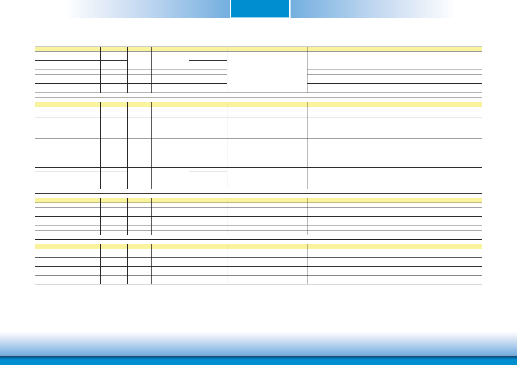
LPC Signals Descriptions
Signal Pin# Pin Type Pwr Rail /Tolerance KB968 Carrier Board Description
LPC_AD0 B4
LPC_AD1 B5
LPC_AD2 B6
LPC_AD3 B7
LPC_FRAME# B3 O CMOS 3.3V / 3.3V LPC frame indicates the start of an LPC cycle
LPC_DRQ0# B8
LPC_DRQ1# B9
LPC_SERIRQ A50 I/O CMOS 3.3V / 3.3V PU 40-50K to 3.3V LPC serial interrupt
LPC_CLK B10 O CMOS 3.3V / 3.3V LPC clock output - 33MHz nominal
SPI Signals Descriptions
Signal Pin# Pin Type Pwr Rail /Tolerance KB968 Carrier Board Description
SPI_CS# B97 O CMOS 3.3V Suspend/3.3V
SPI_MISO A92 I CMOS 3.3V Suspend/3.3V
SPI_MOSI A95 O CMOS 3.3V Suspend/3.3V
SPI_CLK A94 O CMOS 3.3V Suspend/3.3V
SPI_POWER A91 O 3.3V Suspend/3.3V
BIOS_DIS0#
BIOS_DIS1# B88
GA Signals Descriptions
Signal Pin# Pin Type Pwr Rail /Tolerance KB968 Carrier Board Description
VGA_RED B89 O Analog Analog PD 150R to GND PD 150R Red for monitor. Analog output
VGA_GRN B91 O Analog Analog PD 150R to GND PD 150R Green for monitor. Analog output
VGA_BLU B92 O Analog Analog PD 150R to GND PD 150R Blue for monitor. Analog output
VGA_HSYNC B93 O CMOS 3.3V / 3.3V PD 1K to GND Horizontal sync output to VGA monitor
VGA_VSYNC B94 O CMOS 3.3V / 3.3V Vertical sync output to VGA monitor
VGA_I2C_CK B95 I/O OD CMOS 3.3V / 3.3V PU 4.7K to 3.3V DDC clock line (I2C port dedicated to identify VGA monitor capabilities)
VGA_I2C_DAT B96 I/O OD CMOS 3.3V / 3.3V PU 4.7K to 3.3V DDC data line.
Serial Interface Si
Signal Pin# Pin Type Pwr Rail /Tolerance KB968 Carrier Board Description
SER0_TX A98 O CMOS 5V/5V PD 4.7K General purpose serial port 0 transmitter
SER0_RX A99 I CMOS 3.3V/5V PU 47K to 3.3V General purpose serial port 0 receiver
SER1_TX A101 O CMOS 5V/5V PD 4.7K General purpose serial port 1 transmitter
SER1_RX A102 I CMOS 3.3V/5V PU 47K to 3.3V General purpose serial port 1 receiver
nals Descriptions
34
I/O CMOS 3.3V / 3.3V
I CMOS
I CMOS
3.3V / 3.3V LPC serial DMA request
NA
Connect to LPC device
Connect a series resistor 33
Board SPI Device CS# pin
Connect a series resistor 33
Board SPI Device SO pin
Connect a series resistor 33
Board SPI Device SI pin
Connect a series resistor 33
Board SPI Device SCK pin
to Carrier
to Carrier
to Carrier
to Carrier
LPC multiplexed address, command and data bus
Chip select for Carrier Board SPI - may be sourced from chipset SPI0 or SPI1
Data in to Module from Carrier SPI
Data out from Module to Carrier SPI
Clock from Module to Carrier SPI
Power supply for Carrier Board SPI – sourced from Module – nominally
3.3V. The Module shall provide a minimum of 100mA on SPI_POWER.
Carriers shall use less than 100mA of SPI_POWER. SPI_POWER
shall only be used to power SPI devices on the Carrier
Selection straps to determine the BIOS boot device.
The Carrier should only float these or pull them low, please refer to
COM Express Module Base Specification Revision 2.1 for strapping options of BIOS disable signals.
23
www.dfi .comChapter 3 Hardware Installation
Page 24
Chapter 3
S
g
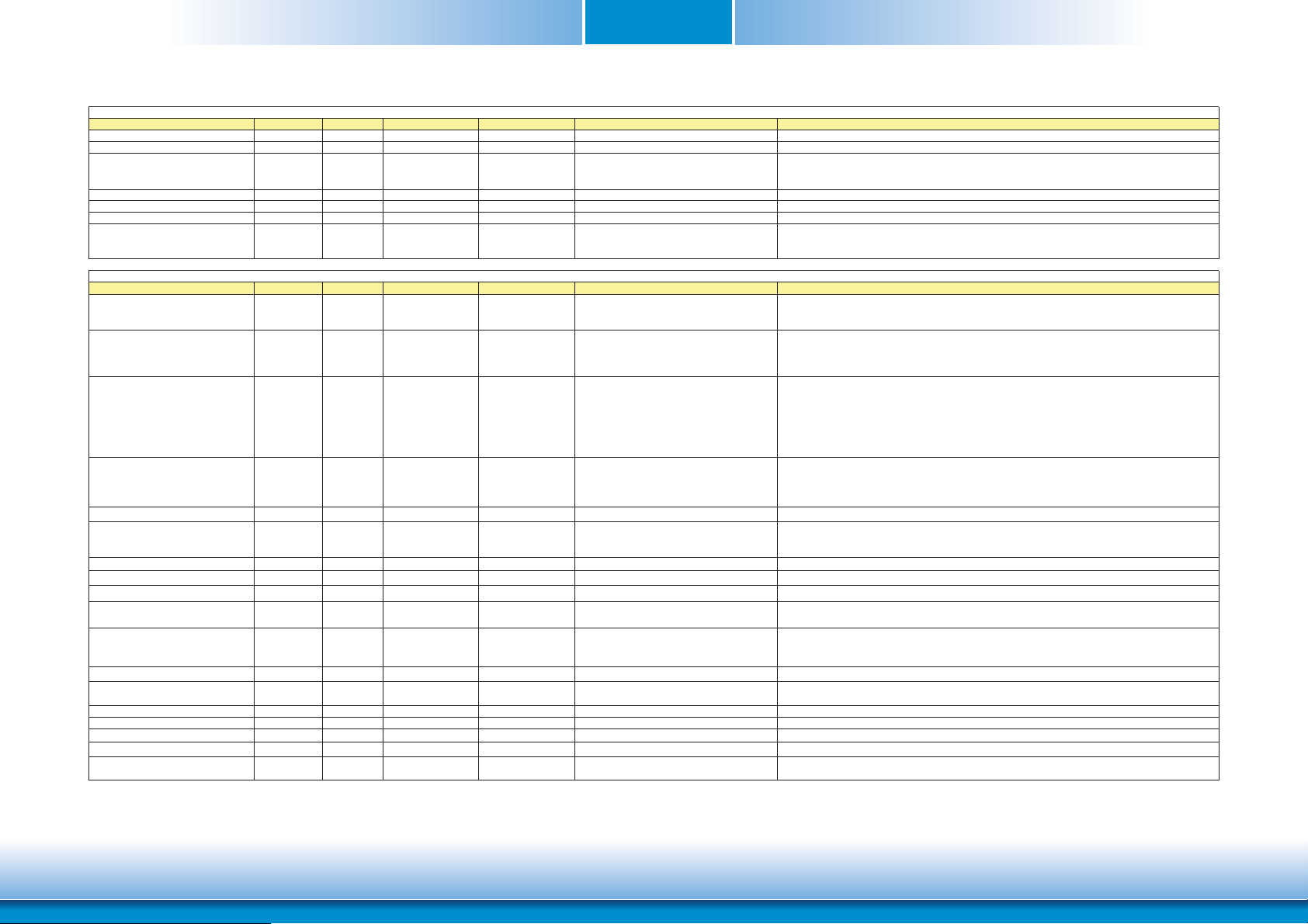
Miscellaneous Si
Signal Pin# Pin Type Pwr Rail /Tolerance KB968 Carrier Board Description
I2C_CK B33 I/O OD CMOS 3.3V Suspend/3.3V PU 2.2K to 3.3VSB General purpose I2C port clock output
I2C_DAT B34 I/O OD CMOS 3.3V Suspend/3.3V PU 2.2K to 3.3VSB General purpose I2C port data I/O line
SPKR B32 O CMOS 3.3V / 3.3V
WDT B27 O CMO
FAN_PWNOUT B101 O CMOS 3.3V / 12V PD 100K to GND Do NOT PU Fan speed control. Uses the Pulse Width Modulation (PWM) technique to control the fan's RPM.
FAN_TACHIN B102 I OD CMOS 3.3V / 12V PU 10K to 3.3V Fan tachometer input for a fan with a two pulse output.
TPM_PP A96 I CMOS 3.3V / 3.3V
Power and System Management Signals Descriptions
Signal Pin# Pin Type Pwr Rail /Tolerance KB968 Carrier Board Description
PWRBTN# B12 I CMOS 3.3V Suspend/3.3V PU 10K to 3.3VSB
SYS_RESET# B49 I CMOS 3.3V Suspend/3.3V PU 40-50K to 3.3VSB
CB_RESET# B50 O CMOS 3.3V Suspend/3.3V PD 100K to GND
PWR_OK B24 I CMOS 3.3V / 3.3V PU 10K to 3.3V
SUS_STAT# B18 O CMOS 3.3V Suspend/3.3V Indicates imminent suspend operation; used to notify LPC devices.
SUS_S3# A15 O CMOS 3.3V Suspend/3.3V
SUS_S4# A18 O CMOS 3.3V Suspend/3.3V Indicates system is in Suspend to Disk state. Active low output.
SUS_S5# A24 O CMOS 3.3V Suspend/3.3V Indicates system is in Soft Off state.
WAKE0# B66 I CMOS 3.3V Suspend/3.3V PU 10K to 3.3VSB PCI Express wake up signal.
WAKE1# B67 I CMOS 3.3V Suspend/3.3V PU 40-50K to 3.3VSB
BATLOW# A27 I CMOS 3.3V Suspend/ 3.3V PU 10K to 3.3VSB
LID# A103 I OD CMOS 3.3V Suspend/12V LID switch. Low active signal used by the ACPI operating system for a LID switch.
SLEEP# B103 I OD CMOS 3.3V Suspend/12V PU 10K to 3.3VSB
THRM# B35 I CMOS 3.3V / 3.3V PU 10K to 3.3V Input from off-Module temp sensor indicating an over-temp situation.
THRMTRIP# A35 O CMOS 3.3V / 3.3V PU 10K to 3.3V NA Active low output indicating that the CPU has entered thermal shutdown.
SMB_CK B13 I/O OD CMOS 3.3V Suspend/3.3V PU 2.2K to 3.3VSB System Management Bus bidirectional clock line.
SMB_DAT B14 I/O OD CMOS 3.3V Suspend/3.3V PU 2.2K to 3.3VSB System Management Bus bidirectional data line.
SMB_ALERT# B15 I CMOS 3.3V Suspend/3.3V
nal Descriptions
Output for audio enunciator - the "speaker" in PC-AT systems.
This port provides the PC beep signal and is mostly intended for
3.3V / 3.3V Output indicating that a watchdog time-out event has occurred.
debugging purposes.
Trusted Platform Module (TPM) Physical Presence pin. Active high.
TPM chip has an internal pull down. This signal is used to indicate
Physical Presence to the TPM.
A falling edge creates a power button event. Power button events can
be used to bring a system out of S5 soft off and other suspend states,
as well as powering the system down.
Reset button input. Active low request for Module to reset and reboot.
May be falling edge sensitive. For situations when SYS_RESET# is
not able to reestablish control of the system, PWR_OK or a power
cycle may be used.
Reset output from Module to Carrier Board. Active low. Issued by
Module chipset and may result from a low SYS_RESET# input, a low
PWR_OK input, a VCC_12V power input that falls below the minimum
specification, a watchdog timeout, or may be initiated by the Module
software.
Power OK from main power supply. A high value indicates that the
power is good. This signal can be used to hold off Module startup to
allow Carrier based FPGAs or other configurable devices time to be
programmed.
Indicates system is in Suspend to RAM state. Active low output. An
inverted copy of SUS_S3# on the Carrier Board may be used to
enable the non-standby power on a typical ATX supply.
General purpose wake up signal. May be used to implement wake-up
on PS2 keyboard or mouse activity.
Indicates that external battery is low.
This port provides a battery-low signal to the Module for orderly
transitioning to power saving or power cut-off ACPI modes.
Sleep button. Low active signal used by the ACPI operating system to bring the
system to sleep state or to wake it up again.
System Management Bus Alert – active low input can be used to
generate an SMI# (System Management Interrupt) or to wake the system.
24
www.dfi .comChapter 3 Hardware Installation
Page 25
Chapter 3
g
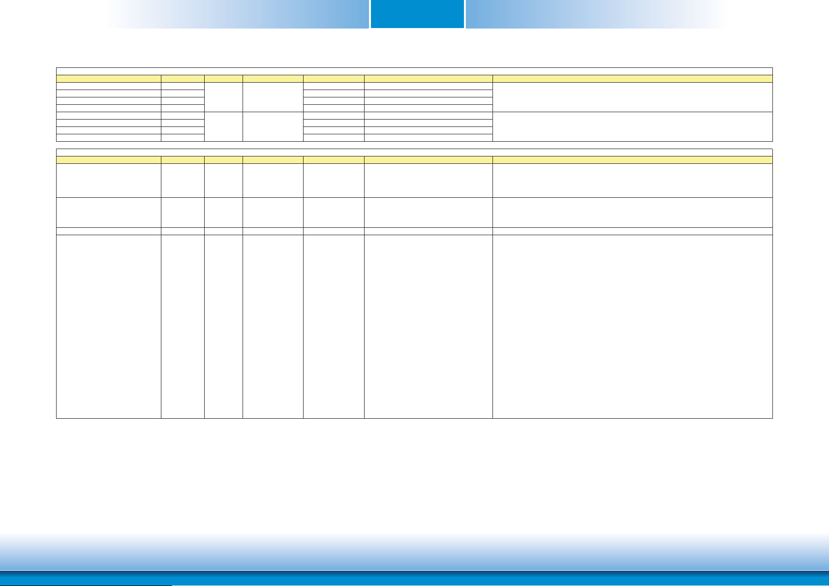
GPIO Si
Signal Pin# Pin Type Pwr Rail /Tolerance KB968 Carrier Board Description
GPO0 A93
GPO1 B54
GPO2 B57
GPO3 B63
GPI0 A54 PU 100K to 3.3V
GPI1 A63 PU 100K to 3.3V
GPI2 A67 PU 100K to 3.3V
GPI3 A85 PU 100K to 3.3V
Power and GND Signal Descriptions
Signal Pin# Pin Type Pwr Rail /Tolerance KB968 Carrier Board Description
VCC_12V
VCC_5V_SBY B84~B87 Power
VCC_RTC A47 Power Real-time clock circuit-power input. Nominally +3.0V.
GND
nals Descriptions
A104~A109
B104~B109
C104~C109
D104~D109
A1, A11, A21,
A31, A41, A51,
A57, A60, A66,
A70, A80, A90,
A100, A110, B1,
B11, B21 ,B31,
B41, B51, B60,
B70, B80, B90,
B100, B110, C1,
C2, C5, C8,
C11, C14, C21,
C31, C41, C51,
C60, C70, C73,
C76, C80, C84,
C87, C90, C93,
C96, C100,
C103, C110,
D1, D2, D5, D8,
D11, D14, D21,
D31, D51, D60,
D67, D70, D73,
D76, D80, D84,
D87, D90, D93,
D96, D100,
D103, D110
O CMOS General purpose output pins.3.3V / 3.3V
I CMOS 3.3V / 3.3V General purpose input pins.
Power Primary power input: +12V nominal. All available VCC_12V pins on the connector(s) shall be used.
Standby power input: +5.0V nominal. If VCC5_SBY is used, all
available VCC_5V_SBY pins on the connector(s) shall be used. Only
used for standby and suspend functions. May be left unconnected if
these functions are not used in the system design.
Power
Ground - DC power and signal and AC signal return path.
All available GND connector pins shall be used and tied to Carrier
Board GND plane.
25
www.dfi .comChapter 3 Hardware Installation
Page 26
Chapter 3
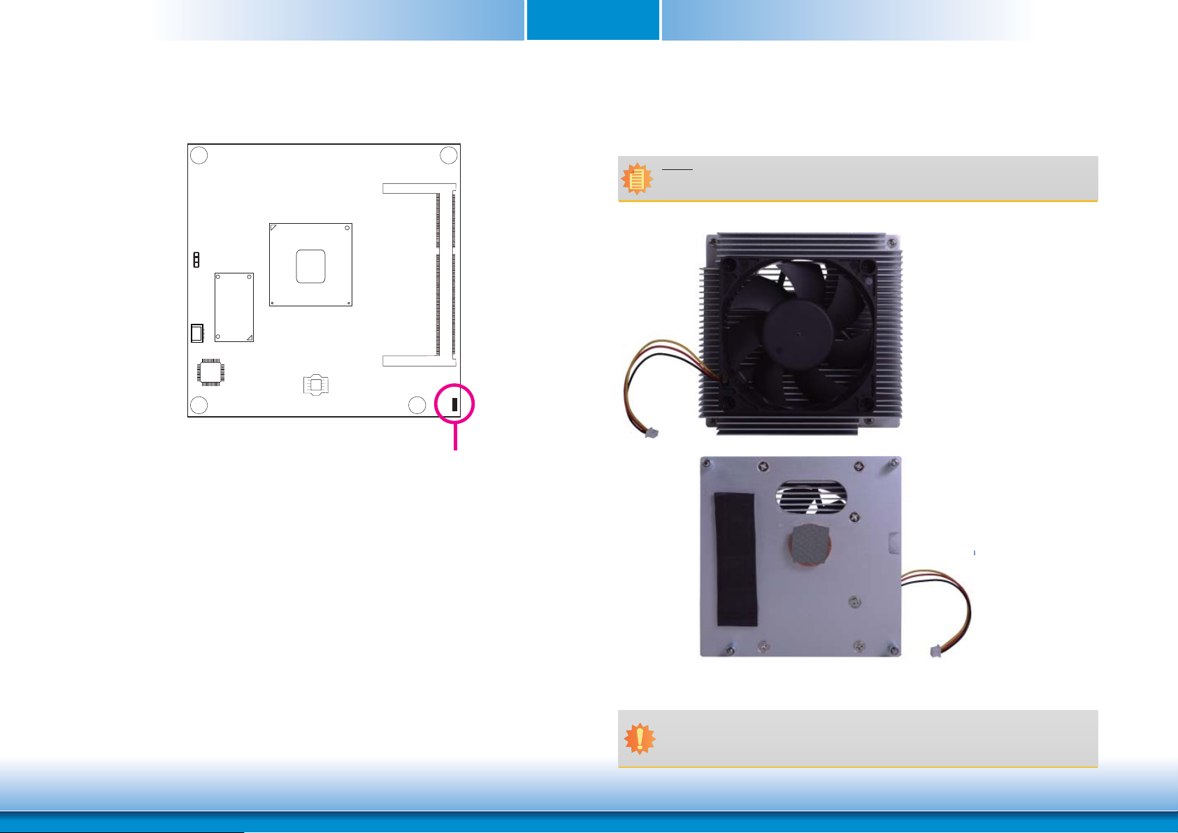
Standby Power LED
This LED will light when the system is in the standby mode.
Cooling Option
Heat Sink with Cooling Fan
Note:
The system board used in the following illustrations may not resemble the actual
board. These illustrations are for reference only.
Top View of the Heat Sink
Standby
Power LED
12
• “1” and “2” denote the locations of the thermal pads designed to contact
the corresponding components that are on KB968.
Important:
Remove the plastic covering from the thermal pads prior to mounting the heat sink
onto KB968.
26
Bottom View of the Heat Sink
www.dfi .comChapter 3 Hardware Installation
Page 27
Chapter 3
Installing KB968 onto a Carrier Board
Important:
The carrier board (COM331-B) used in this section is for reference purpose only and
may not resemble your carrier board. These illustrations are mainly to guide you on
how to install KB968 onto the carrier board of your choice.
• To download COM331-B datasheet and manual
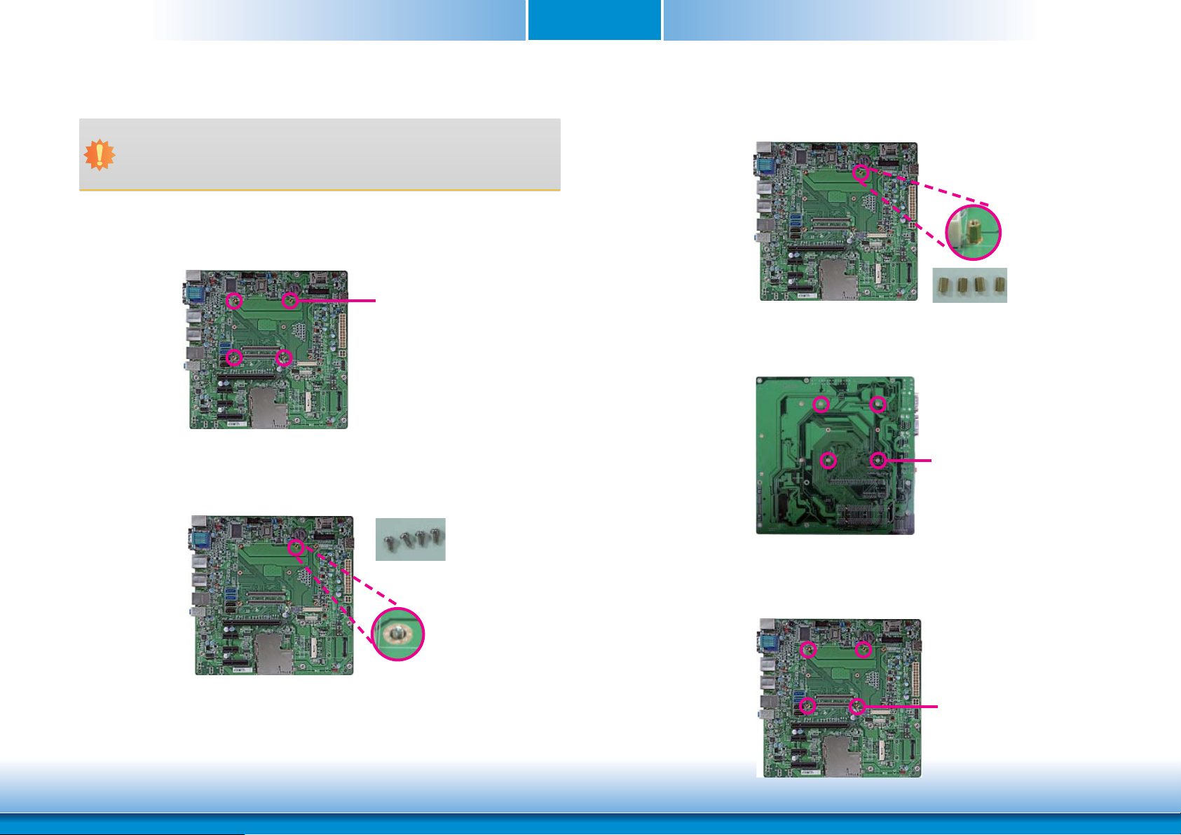
1. Now install the module and heatsink assembly onto the carrier board. The photo below
shows the locations of the mounting holes on carrier board.
2. Insert the provided mounting screws into the mounting holes - from the bottom through
the top of the carrier board.
Mounting hole
3. While supporting the mounting screw at the bottom, from the top side of the board, fasten
a bolt into the screw.
Bolts
4. The photo below shows the solder side of the board with the screws already fixed in place.
Mounting screw
Mounting screws
5. The photo below shows the component side of the board with the bolts already fixed in
place.
Bolts
27
www.dfi .comChapter 3 Hardware Installation
Page 28

Chapter 3
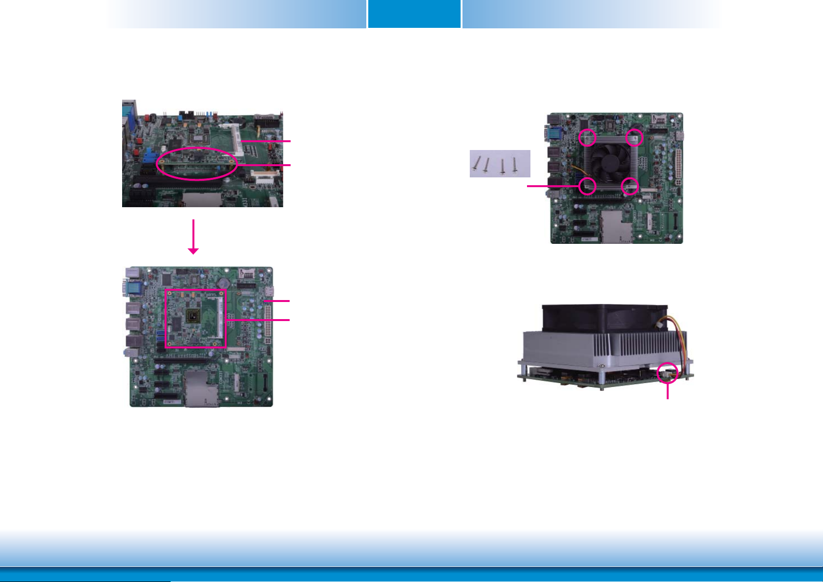
6. Grasping KB968 by its edges, position it on top of the carrier board with its mounting
holes aligned with the bolts on the carrier board. This will also align the COM Express
connectors of the two boards to each other.
COM Express connectors
on KB968
COM Express connectors
on the carrier board
7. Press KB968 down firmly until it is completely seated on the COM Express connectors of
the carrier board.
KB968
COM Express connectors
on the carrier board
Pressing points
BIOS ROM socket
Note:
The above illustration shows the pressing points of the module onto the carrier board.
e careful when pressing the module, it may damage the socket.
B
28
www.dfi .comChapter 3 Hardware Installation
Page 29
Chapter 3
8. Verify that the module is firmly seated onto the COM Express connectors of the carrier
board.
KB968
The module is completely
seated on the carrier board
Carrier board
KB968
9. Use the provided mounting screws to secure KB968 with heat sink to the carrier board
and then connect the cooling fan’s cable to the fan connector on KB968. The photo below
shows the locations of the long mounting screws.
Long screws
10. And then connect the cooling fan’s cable to the fan connector on KB968.
Fan connector
29
www.dfi .comChapter 3 Hardware Installation
Page 30
Chapter 3
Installing the COM Express Debug Card
Note:
The system board used in the following illustrations may not resemble the actual
board. These illustrations are for reference only.
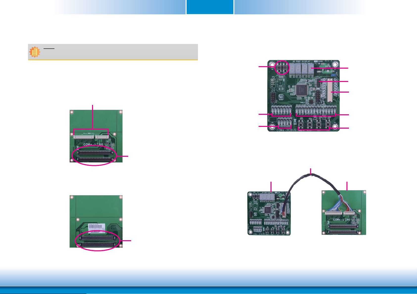
1. COMe-LINK1 is the COM Express debug card designed for COM Express Compact modules
to debug and display signals and codes of COM Express modules.
COMe-LINK1
COMe-DEBUG Connector
COM Express
Connectors
Top view
2. Connect the COMe-DEBUG card to COMe-LINK1 via a cable.
COMe-DEBUG
Code Review
Control
COM Express
Type Display
COM Express
Power Display
Cable
COMe-DEBUG COMe-LINK1
80 Port Display
LPC
COMe-LINK1/2
Connector
COM Express
Signal Display
Power/Reset/
Sleep/LID control
Bottom view
COM Express
Connectors
30
www.dfi .comChapter 3 Hardware Installation
Page 31
Chapter 3
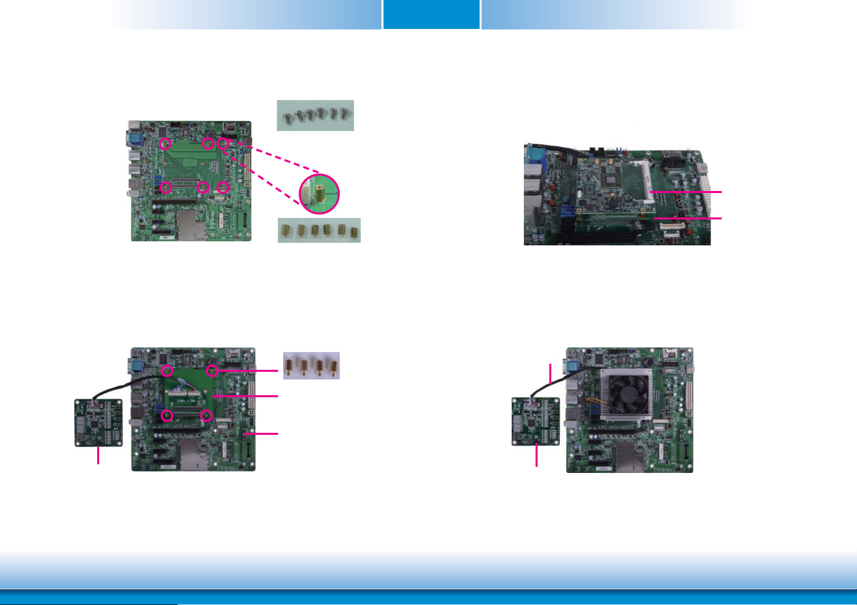
3. Fasten bolts with mounting screws through mounting holes to be fixed in place.
Mounting screws
Bolts
4. Use the provided bolts to fix the COMe-LINK1 debug card onto the carrier board.
Bolts
5. Grasp KB968 by its edges to press it down on the top of the COMe-LINK1 debug card.
KB968
COMe-LINK1
6. Then, grasp the heat sink by its edges and position it down firmly on the top of the
KB968.
Cable
COMe-DEBUG
COMe-LINK1
Carrier Board
COMe-DEBUG
31
www.dfi .comChapter 3 Hardware Installation
Page 32
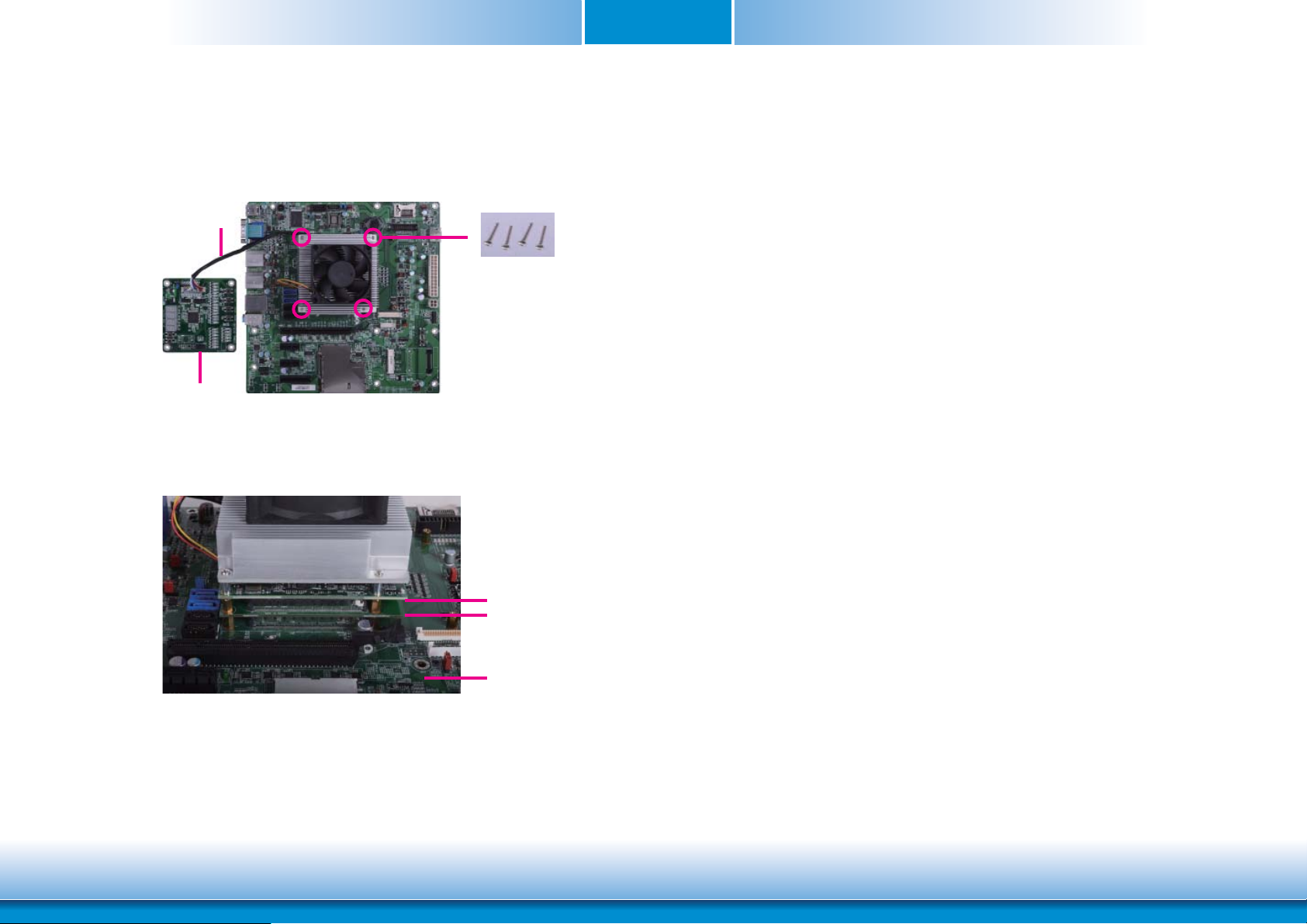
7. Use the long mounting screws to secure the heat sink on the top of the KB968 and the
COMe-LINK1 debug card and connect the cooling fan’s cable to the fan connector on
KB968. The photo below shows the locations of long mounting screws.
Cable
COMe-DEBUG
Long screws
Chapter 3
COM Express Module
COMe-LINK1
Carrier Board
Side View of the Module, Debug Card and Carrier Board
32
www.dfi .comChapter 3 Hardware Installation
Page 33
Chapter 4
Chapter 4 - BIOS Setup
Overview
The BIOS is a program that takes care of the basic level of communication between the CPU
and peripherals. It contains codes for various advanced features found in this system board.
The BIOS allows you to configure the system and save the configuration in a battery-backed
CMOS so that the data retains even when the power is off. In general, the information stored
in the CMOS RAM of the EEPROM will stay unchanged unless a configuration change has been
made such as a hard drive replaced or a device added.
It is possible that the CMOS battery will fail causing CMOS data loss. If this happens, you need
to install a new CMOS battery and reconfigure the BIOS settings.
Note:
The BIOS is constantly updated to improve the performance of the system board;
therefore the BIOS screens in this chapter may not appear the same as the actual
one. These screens are for reference purpose only.
Default Configuration
Most of the configuration settings are either predefined according to the Load Optimal Defaults
settings which are stored in the BIOS or are automatically detected and configured without
requiring any actions. There are a few settings that you may need to change depending on
your system configuration.
Entering the BIOS Setup Utility
The BIOS Setup Utility can only be operated from the keyboard and all commands are keyboard commands. The commands are available at the right side of each setup screen.
The BIOS Setup Utility does not require an operating system to run. After you power up the
system, the BIOS message appears on the screen and the memory count begins. After the
memory test, the message “Press DEL to run setup” will appear on the screen. If the message
disappears before you respond, restart the system or press the “Reset” button. You may also
restart the system by pressing the <Ctrl> <Alt> and <Del> keys simultaneously.
Legends
Keys Function
Right and Left arrows
Up and Down arrows
<Esc>
+ (plus key)
- (minus key)
Tab
<F1>
<F2>
<F3>
<F4>
<Enter>
Moves the highlight left or right to select a menu.
Moves the hightlight up or down between submenu or fi elds.
Exit to the BIOS Setup Utility.
Scrolls forward through the values or options of the highlighted
fi eld.
Scrolls backward through the values or options of the highlighted
fi eld.
Select a fi eld.
Displays general help
Pervious values
Optimized defaults
Saves and resets the setup program.
Press <Enter> to enter the highlighted submenu.
Scroll Bar
When a scroll bar appears to the right of the setup screen, it indicates that there are more
available fields not shown on the screen. Use the up and down arrow keys to scroll through all
the available fields.
Submenu
When ““ appears on the left of a particular field, it indicates that a submenu which contains
additional options are available for that field. To display the submenu, move the highlight to
that field and press <Enter>.
33
www.dfi .comChapter 4 BIOS Setup
Page 34

Chapter 4
AMI BIOS Setup Utility Advanced Main
The Main menu is the first screen that you will see when you enter the BIOS Setup Utility.
Main
BIOS Information
BIOS Vendor
Build Date and Time
Memory Information
Total Memory
System Lanuage
System Date
System Time
Access Level
System Date
The date format is <day>, <month>, <date>, <year>. Day displays a day, from Sunday to Saturday. Month displays the month, from January to December. Date displays
the date, from 1 to 31. Year displays the year, from 1980 to 2099.
Aptio Setup Utility - Copyright (C) 2013 American Megatrends, Inc.
Advanced
Version 2.16.1240. Copyright (C) 2013 American Megatrends, Inc.
Boot Security
American Megatrends
12/17/2013 16:25:49
2048MB (DDR3)
[English]
[Fri 17/01/2014]
[13:45:30]
Administraor
Save & ExitChipset
Choose the system default
language.
Select Screen
Select Item
Enter:
Select
+/-:
Change Opt.
F1:
General Help
F2:
Previous Values
F3:
Optimized Defaults
F4:
Save Changes and
Reset
ESC:
Exit
The Advanced menu allows you to configure your system for basic operation. Some entries are
defaults required by the system board, while others, if enabled, will improve the performance
of your system or let you set some features according to your preference.
Important:
Setting incorrect field values may cause the system to malfunction
Main
ACPI Settings
Trusted Computing
DFI Wakeup Confi guration
PC Health Status
CPU Confi guration
DDR3 Voltage Setting
IDE Confi guration
USB Confi guration
Network Stack
WatchDog Confi guration
Intel(R) I210 Gigabit Network Connection - 00:01:29:53......
Aptio Setup Utility - Copyright (C) 2013 American Megatrends, Inc.
Advanced
Version 2.16.1240. Copyright (C) 2013 American Megatrends, Inc.
Save & ExitChipset Boot Security
System ACPI Parameters.
Enter:
+/-:
F1:
F2:
F3:
F4:
ESC:
.
Select Screen
Select Item
Select
Change Opt.
General Help
Previous Values
Optimized Defaults
Save Changes and
Reset
Exit
System Time
The time format is <hour>, <minute>, <second>. The time is based on the 24-hour
military-time clock. For example, 1 p.m. is 13:00:00. Hour displays hours from 00 to
23. Minute displays minutes from 00 to 59. Second displays seconds from 00 to 59.
34
www.dfi .comChapter 4 BIOS Setup
Page 35
Chapter 4
ACPI Settings
This section is used to configure the ACPI settings.
Aptio Setup Utility - Copyright (C) 2013 American Megatrends, Inc.
Advanced
ACPI Settings
Enable ACPI Auto Confi guration
Enable Hibernation
ACPI Sleep State
Version 2.16.1240. Copyright (C) 2013 American Megatrends, Inc.
[Disabled]
[Enabled]
[S3 Only (Suspend to ....) ]
Enables or Disables BIOS
ACPI Auto Confi guration.
Select Screen
Select Item
Enter:
Select
+/-:
Change Opt.
F1:
General Help
F2:
Previous Values
F3:
Optimized Defaults
F4:
Save Changes and
Reset
ESC:
Exit
Enable ACPI Auto Configuration
Enables or disables BIOS ACPI Auto Configuration.
Enable Hibernation
When this function is enabled, the system will enter the hibernate mode (OS/S4 sleep
state). This function is not applicable to some OS.
Trusted Computing
This section sets the trusted computing function.
Aptio Setup Utility - Copyright (C) 2013 American Megatrends, Inc.
Advanced
Confi guration
Security Device Support
Current Status Information
No Security Device Found
Version 2.16.1240. Copyright (C) 2013 American Megatrends, Inc.
[Disable]
Security Device Support
This field is used to enable or disable BIOS supporting for the security device. O.S will
not show the security device. TCG EFI protocol and INT1A interface will not be
available.
Enables or Disables
BIOS support for security
device. O.S will not show
Security Device. TCG
EFI protocol and INT1A
interface will not be
available.
Select Screen
Select Item
Enter:
Select
+/-:
Change Opt.
F1:
General Help
F2:
Previous Values
F3:
Optimized Defaults
F4:
Save Changes and
Reset
ESC:
Exit
ACPI Sleep State
Selects the ACPI sleep state that the system will enter when the Suspend button is
pressed.
S3 Only (STR) Enables the Suspend to RAM function.
35
www.dfi .comChapter 4 BIOS Setup
Page 36
Chapter 4
DFI Wakeup Configuration
This section configures the DFI wakeup ACPI power management.
Aptio Setup Utility - Copyright (C) 2013 American Megatrends, Inc.
Advanced
DFI Wakeup ACPI Power Management Confi guation
Resume by PME
Resume by USB
Version 2.16.1240. Copyright (C) 2013 American Megatrends, Inc.
[Disabled]
[Enabled]
About Resume by PME
(PCI, PCIE, LAN)
Enter:
+/-:
F1:
F2:
F3:
F4:
ESC:
Resume by PME
Enables this field to use the PME signal to wake up the system.
Resume by USB
Enables this field to use the USB signal to wake up the system.
Select Screen
Select Item
Select
Change Opt.
General Help
Previous Values
Optimized Defaults
Save Changes and
Reset
Exit
PC Health Status
This section displays hardware health monitor.
Aptio Setup Utility - Copyright (C) 2013 American Megatrends, Inc.
Advanced
System Hardware Monitor
CPU Temperature
CPU FAN Speed
APU_VDD
APU_VDDNB
+1.5V DDR3
+1V8
+0V95
EC Version
Version 2.16.1240. Copyright (C) 2013 American Megatrends, Inc.
: +40 C
: N/A
: +1.281V
: +0.944 V
: +1.516V
: +1.797 V
: +0.953 V
2013.10.01.11
Select Screen
Select Item
Enter:
Select
+/-:
Change Opt.
F1:
General Help
F2:
Previous Values
F3:
Optimized Defaults
F4:
Save Changes and
Reset
ESC:
Exit
36
www.dfi .comChapter 4 BIOS Setup
Page 37
Chapter 4
CPU Configuration
This section is used to configure the CPU. It will also display the detected CPU information.
Aptio Setup Utility - Copyright (C) 2013 American Megatrends, Inc.
Advanced
CPU Confi guration
Module Version: 4.6.5.3 KabiniPI 018
AGESA Version: 1.0.0.8
NX Mode
SVM Mode
Core Leveling Mode
Node 0 Information
Version 2.16.1240. Copyright (C) 2013 American Megatrends, Inc.
[Enabled]
[Enabled]
[Automatic mode]
Enable/disable No-execute
page protection function
Select Screen
Select Item
Enter:
Select
+/-:
Change Opt.
F1:
General Help
F2:
Previous Values
F3:
Optimized Defaults
F4:
Save Changes and
Reset
ESC:
Exit
NX Mode
Enables or disables the function of the No-execute page proection.
SVM Mode
Enables or disables the CPU virtualization.
Node 0 Information
This field only displays the memory information related to Node 0.
Aptio Setup Utility - Copyright (C) 2013 American Megatrends, Inc.
Advanced
Socket0: AMD GX-420CA SOC with Radeon(tm) HD Graphics
Quad Core Running @ 2031MHz 1300 mV
Max Speed: 2000MHz Intended Speed: 2000MHz
Min Speed: 1800MHz
Microcode Patch Level: 700010b
--------Cache per Compute Unit---------------L1 Instruction Cache: 128 KB/2-way
L1 Data Cache: 128 KB/8-way
L2 Cache: 2048 KB/16-way
No L3 Cache Present
Version 2.16.1240. Copyright (C) 2013 American Megatrends, Inc.
Select Screen
Select Item
Enter:
Select
+/-:
Change Opt.
F1:
General Help
F2:
Previous Values
F3:
Optimized Defaults
F4:
Save Changes and
Reset
ESC:
Exit
Core Leveling Mode
Changes the number of cores in the system.
37
www.dfi .comChapter 4 BIOS Setup
Page 38
Chapter 4
DDR3 Voltage Setting
This section is used to configure the DD3 voltage setting.
Aptio Setup Utility - Copyright (C) 2013 American Megatrends, Inc.
Advanced
DDR3 Voltage setting
Version 2.16.1240. Copyright (C) 2013 American Megatrends, Inc.
[1.5V]
DDR3 Voltage setting
This field is used to select the DDR3 voltage: 1.5V, 1.35V or 1.25V.
DDR3 Voltage setting
Select Screen
Select Item
Enter:
Select
+/-:
Change Opt.
F1:
General Help
F2:
Previous Values
F3:
Optimized Defaults
F4:
Save Changes and
Reset
ESC:
Exit
IDE Configuration
This section is used to configure the IDE device.
Aptio Setup Utility - Copyright (C) 2013 American Megatrends, Inc.
Advanced
IDE Confi guration
SATA Port 0 Not present
SATA Port 1 Not present
Version 2.16.1240. Copyright (C) 2013 American Megatrends, Inc.
Select Screen
Select Item
Enter:
Select
+/-:
Change Opt.
F1:
General Help
F2:
Previous Values
F3:
Optimized Defaults
F4:
Save Changes and
Reset
ESC:
Exit
38
www.dfi .comChapter 4 BIOS Setup
Page 39
Chapter 4
USB Configuration
This section is used to configure the parameters of the USB device.
Aptio Setup Utility - Copyright (C) 2013 American Megatrends, Inc.
Advanced
USB Confi guration
USB Module Version
USB devices:
2 keyboards
Legacy USB Support
EHCI Hand-off
USB Mass Storage Driver Support
Port 60/64 Emulation
Version 2.16.1240. Copyright (C) 2013 American Megatrends, Inc.
8.10.27
[Enabled]
[Disabled]
[Enabled]
[Enabled]
Enables Legacy USB
support. AUTO option
disables legacy support if
no USB devices are connected. DISABLE option
will keep USB devices
available only for EFI
application.
Enter:
+/-:
F1:
F2:
F3:
F4:
ESC:
Legacy USB Support
Enabled
Enables legacy USB.
Auto
Disables support for legacy when no USB devices are connected.
Disabled
Keeps USB devices available only for EFI applications.
Select Screen
Select Item
Select
Change Opt.
General Help
Previous Values
Optimized Defaults
Save Changes and
Reset
Exit
Network Stack
This section is used to enable or disable UEFI network stack.
Aptio Setup Utility - Copyright (C) 2013 American Megatrends, Inc.
Advanced
Network Stack
Version 2.16.1240. Copyright (C) 2013 American Megatrends, Inc.
[Disabled]
When Network Stack is enabled, it will display the following information:
Aptio Setup Utility - Copyright (C) 2013 American Megatrends, Inc.
Advanced
Network Stack
Ipv4 PXE Support
Ipv6 PXE Support
PXE boot wait time
[Enabled]
[Enabled]
[Enabled]
0
Enable/Disable UEFI
network stack.
Select Screen
Select Item
Enter:
Select
+/-:
Change Opt.
F1:
General Help
F2:
Previous Values
F3:
Optimized Defaults
F4:
Save Changes and
Reset
ESC:
Exit
Enable/Disable UEFI
network stack.
EHCI Hand-off
This is a workaround for OSes without the support of EHCI hand-off. The change of
EHCI ownership should be claimed by the EHCI driver.
USB Mass Storage Driver Support
This field is used to enable or disable the USB Mass storage driver support.
Port 60/64 Emulation
Enables the 60h/64h I/O port emulation. You must enable this to fully support USB
keyboard legacy for non-USB OSes.
Select Screen
Select Item
Enter:
Select
+/-:
Change Opt.
F1:
General Help
F2:
Previous Values
F3:
Optimized Defaults
F4:
Save Changes and
Reset
ESC:
Exit
Version 2.16.1240. Copyright (C) 2013 American Megatrends, Inc.
39
www.dfi .comChapter 4 BIOS Setup
Page 40
Chapter 4
Ipv4 PXE Support
When enabled, Ipv4 PXE boot supports. When disabled, Ipv4 PXE boot option will not
be created.
Ipv6 PXE Support
When enabled, Ipv6 PXE boot supports. When disabled, Ipv6 PXE boot option will not
be created.
PXE boot wait time
Waits time to press ESC key to abort the PXE boot.
WatchDog Configuration
This section is used to configure the parameters of IT8518 WatchDog Timer.
Aptio Setup Utility - Copyright (C) 2013 American Megatrends, Inc.
Advanced
Enable/Disable IT8518
WatchDog1 function
WatchDog2 function
[Disabled]
[Disabled]
Version 2.16.1240. Copyright (C) 2013 American Megatrends, Inc.
WatchDog Timer.
Select Screen
Select Item
Enter:
Select
+/-:
Change Opt.
F1:
General Help
F2:
Previous Values
F3:
Optimized Defaults
F4:
Save Changes and
Reset
ESC:
Exit
WatchDog function
This field is used to enable or disable the Watchdog timer function.
WatchDog1 function
For KB968 module board (Reset KB968 by hardware).
WatchDog2 function
For carrier board usage.
40
www.dfi .comChapter 4 BIOS Setup
Page 41
Chapter 4
Intel(R) I210 Gigabit Network Connection - 00:01:29:53...
This section is used to configure the parameters of the Gigabit Ethernet device.
Aptio Setup Utility - Copyright (C) 2013 American Megatrends, Inc.
Advanced
Click to confi gure the
PORT CONFIGURATION MENU
NIC Confi guration
Blink LEDs (range 0-15 seconds)
PORT CONFIGURATION INFORMATION
UEFI Driver:
Adapter PBA:
Chip Type:
PCI Device ID
PCI Bus: Device: Function:
Link Status
Factory MAC Address:
Alternate MAC Address:
Version 2.16.1240. Copyright (C) 2013 American Megatrends, Inc.
0
Intel(R) 1GbE DEV 5.1.00
001300-000
Intel i210
1533
1:0:0
[Disconnected]
00:01:29:53:84:DA
00:01:29:53:84:DA
network device port.
Select Screen
Select Item
Enter:
Select
+/-:
Change Opt.
F1:
General Help
F2:
Previous Values
F3:
Optimized Defaults
F4:
Save Changes and
Reset
ESC:
Exit
NIC Configuration
This field is used to configure the network device.
Blink LEDs
Blink LEDs for the specified duration (up to 15 seconds).
Chipset
This section configures relevant chipset functions.
Main
GFX Confi guration
South Bridge
North Bridge
North Bridge LVDS Confi g Select
Aptio Setup Utility - Copyright (C) 2013 American Megatrends, Inc.
Advanced
Chipset
Version 2.16.1240. Copyright (C) 2013 American Megatrends, Inc.
Boot Security
Save & Exit
GFX Confi guration
Select Screen
Select Item
Enter:
Select
+/-:
Change Opt.
F1:
General Help
F2:
Previous Values
F3:
Optimized Defaults
F4:
Save Changes and
Reset
ESC:
Exit
Link Status
This field indicates the link status of the network device.
Alternate MAC Address
Alternates assigned MAC address of Ethernet port.
41
www.dfi .comChapter 4 BIOS Setup
Page 42
Chapter 4
GFX Configuration
Aptio Setup Utility - Copyright (C) 2013 American Megatrends, Inc.
Chipset
GFX Confi guration
Primary Video Device
Integrated Graphics
Version 2.16.1240. Copyright (C) 2013 American Megatrends, Inc.
[NB PCIe Slot Video]
[Auto]
Primary Video Device
Selects the primary video device: IGD Video or NB PCIe Slot Video.
Integrated Graphics
Enables the integrated graphics controller.
Select Primary Video
Device. That BIOS Will
Use To For Output.
Select Screen
Select Item
Enter:
Select
+/-:
Change Opt.
F1:
General Help
F2:
Previous Values
F3:
Optimized Defaults
F4:
Save Changes and
Reset
ESC:
Exit
South Bridge
Aptio Setup Utility - Copyright (C) 2013 American Megatrends, Inc.
Chipset
SB SATA Confi guration
SB USB Confi guration
SB HD Azalia Confi guration
Version 2.16.1240. Copyright (C) 2013 American Megatrends, Inc.
Options For SATA Confi guration
Select Screen
Select Item
Enter:
Select
+/-:
Change Opt.
F1:
General Help
F2:
Previous Values
F3:
Optimized Defaults
F4:
Save Changes and
Reset
ESC:
Exit
42
www.dfi .comChapter 4 BIOS Setup
Page 43
Chapter 4
SB SATA Configuration
Aptio Setup Utility - Copyright (C) 2013 American Megatrends, Inc.
Chipset
OnChip SATA Channel
OnChip SATA Type
Version 2.16.1240. Copyright (C) 2013 American Megatrends, Inc.
[Enable]
[Native IDE]
Select Screen
Select Item
Enter:
Select
+/-:
Change Opt.
F1:
General Help
F2:
Previous Values
F3:
Optimized Defaults
F4:
Save Changes and
Reset
ESC:
Exit
OnChip SATA Type
This field is used to select the onchip SATA type: Native IDE, AHCI or Legacy IDE
SB USB Configuration
Aptio Setup Utility - Copyright (C) 2013 American Megatrends, Inc.
Chipset
XHCI Controller 0
OHCI HC (Bus 0 Dev 18 Fn 0)
EHCI HC (Bus 0 Dev 18 Fn 2)
OHCI HC (Bus 0 Dev 19 Fn 0)
EHCI HC (Bus 0 Dev 19 Fn 2)
USB Port 0
USB Port 1
USB Port 2
USB Port 3
USB Port 4
USB Port 5
USB Port 8
USB Port 9
Version 2.16.1240. Copyright (C) 2013 American Megatrends, Inc.
[Enabled]
[Enabled]
[Enabled]
[Enabled]
[Enabled]
[Enabled]
[Enabled]
[Enabled]
[Enabled]
[Enabled]
[Enabled]
[Enabled]
[Enabled]
.
XHCI Enable Help
Select Screen
Select Item
Enter:
Select
+/-:
Change Opt.
F1:
General Help
F2:
Previous Values
F3:
Optimized Defaults
F4:
Save Changes and
Reset
ESC:
Exit
43
www.dfi .comChapter 4 BIOS Setup
Page 44
Chapter 4
SB HD Azalia Configuration
Aptio Setup Utility - Copyright (C) 2013 American Megatrends, Inc.
Chipset
HD Audio Azalia Device
Version 2.16.1240. Copyright (C) 2013 American Megatrends, Inc.
[Enabled]
Select Screen
Select Item
Enter:
Select
+/-:
Change Opt.
F1:
General Help
F2:
Previous Values
F3:
Optimized Defaults
F4:
Save Changes and
Reset
ESC:
Exit
North Bridge
North Bridge Confi guration
Memory Clock
Memory Clear
Memory ECC Feature
Memory Information
Memory Clock: 800MHz
Total Memory: 2048MB (DDR3)
Memory Clock
This field allows user to select different memory clock. Default value is Auto.
Memory Clear
Memory clear functionality control.
Memory ECC Feature
Enables or disables the memory ECC feature.
Aptio Setup Utility - Copyright (C) 2013 American Megatrends, Inc.
Memory Confi guration
Socket 0 Information
Version 2.16.1240. Copyright (C) 2013 American Megatrends, Inc.
Chipset
[Auto]
[Cleared]
[Enabled]
Memory Clock
Auto
800MHz
1066MHz
1333MHz
1600MHz
This option allows user to
select different memory
clock. Default value is
800MHz.
Select Screen
Select Item
Enter:
Select
+/-:
Change Opt.
F1:
General Help
F2:
Previous Values
F3:
Optimized Defaults
F4:
Save Changes and
Reset
ESC:
Exit
44
www.dfi .comChapter 4 BIOS Setup
Page 45
Chapter 4
Memory Configuration
Aptio Setup Utility - Copyright (C) 2013 American Megatrends, Inc.
Chipset
Memory Confi guration
Memory Hole Remapping
Memory Hole 15MB-16MB
Version 2.16.1240. Copyright (C) 2013 American Megatrends, Inc.
[Enabled]
[Disabled]
Memory Hole 15MB-16MB
Memory Hole 15MB-16MB for some ISA expansion cards
Memory Hole Remapping.
Select Screen
Select Item
Enter:
Select
+/-:
Change Opt.
F1:
General Help
F2:
Previous Values
F3:
Optimized Defaults
F4:
Save Changes and
Reset
ESC:
Exit
.
Socket 0 Information
Aptio Setup Utility - Copyright (C) 2013 American Megatrends, Inc.
Chipset
Socket 0 Information
Starting Address: 0KB
Ending Address: 2097151KB
Dimm1: size = 2048MB, speed = 800MHz
Version 2.16.1240. Copyright (C) 2013 American Megatrends, Inc.
Select Screen
Select Item
Enter:
Select
+/-:
Change Opt.
F1:
General Help
F2:
Previous Values
F3:
Optimized Defaults
F4:
Save Changes and
Reset
ESC:
Exit
45
www.dfi .comChapter 4 BIOS Setup
Page 46
Chapter 4
North Bridge LVDS Config Select
This field is used to specify INT15 options for LVDS interface.
Aptio Setup Utility - Copyright (C) 2013 American Megatrends, Inc.
Chipset
Specify INT15 options for LVDS
DP0 Output Mode
LVDS Panel Confi g Select
Version 2.16.1240. Copyright (C) 2013 American Megatrends, Inc.
[Disabled]
[LVDS Option 1 800x6..]
NB PCIE Connect Type
(Display device).
Select Screen
Select Item
Enter:
Select
+/-:
Change Opt.
F1:
General Help
F2:
Previous Values
F3:
Optimized Defaults
F4:
Save Changes and
Reset
ESC:
Exit
DP0 Output Mode
This field used to select the display device type. When the LVDS mode is selected, it
will display the following information:
Aptio Setup Utility - Copyright (C) 2013 American Megatrends, Inc.
Chipset
Specify INT15 options for LVDS
DP0 Output Mode
LVDS Panel Confi g Select
LVDS Backlight Control
[LVDS]
[LVDS Option 1 800x6..]
127
NB PCIE Connect Type
(Display device).
LVDS Panel Config Select
This option selects the display type for LVDS panel.
Aptio Setup Utility - Copyright (C) 2013 American Megatrends, Inc.
Chipset
Specify INT15 options for LVDS
DP0 Output Mode
LVDS Panel Confi g Select
LVDS Backlight Control
Version 2.16.1240. Copyright (C) 2013 American Megatrends, Inc.
[LVDS]
[LVDS Option 1 800x6..]
127
LCD Panel Confi g Select
LVDS Option 1
LVDS Option 2
LVDS Option 3
LVDS Option 4
LVDS Option 5
LVDS Option 6
LVDS Option 7
LVDS Option 8
LVDS Option 9
800x600
1024x768
1280x720
1280x800
1280x1024
1366x768
1440x900
1600x900
1920x1024
LVDS Backlight Control
LVDS backlight control range: 0 to 255.
Select Screen
Select Item
Enter:
Select
+/-:
Change Opt.
F1:
General Help
F2:
Previous Values
F3:
Optimized Defaults
F4:
Save Changes and
Reset
ESC:
Exit
Enter:
+/-:
F1:
F2:
F3:
F4:
ESC:
Version 2.16.1240. Copyright (C) 2013 American Megatrends, Inc.
Select Screen
Select Item
Select
Change Opt.
General Help
Previous Values
Optimized Defaults
Save Changes and
Reset
Exit
46
www.dfi .comChapter 4 BIOS Setup
Page 47
Chapter 4
Boot
Main
Boot Confi guration
Setup Prompt Timeout
Bootup NumLock State
Quiet Boot
Boot Option Priorities
CSM Parameters
Aptio Setup Utility - Copyright (C) 2013 American Megatrends, Inc.
Advanced
Version 2.16.1240. Copyright (C) 2013 American Megatrends, Inc.
Boot
1
[On]
[Disabled]
Security
Save & ExitChipset
Number of seconds to
wait for setup activation
key.
65535(0xFFFF) means
indefi nite waiting.
Select Screen
Select Item
Enter:
Select
+/-:
Change Opt.
F1:
General Help
F2:
Previous Values
F3:
Optimized Defaults
F4:
Save Changes and
Reset
ESC:
Exit
Setup Prompt Timeout
Selects the number of seconds to wait for the setup activation key. 65535(0xFFFF)
denotes indefinite waiting.
Bootup NumLock State
This allows you to determine the default state of the numeric keypad. By default, the
system boots up with NumLock on wherein the function of the numeric keypad is the
number keys. When set to Off, the function of the numeric keypad is the arrow keys.
Quiet Boot
Enables or disables the quiet boot function.
CSM Parameters
Main
Launch CSM
Boot option fi lter
Launch PXE OpROM policy
Launch Storage OpROM policy
Launch Video OpROM policy
Other PCI device ROM priority
Aptio Setup Utility - Copyright (C) 2013 American Megatrends, Inc.
Advanced
Version 2.16.1240. Copyright (C) 2013 American Megatrends, Inc.
Boot
Security
[Enabled]
[UEFI and Legacy]
[Do not launch]
[Do not launch]
[Legacy only]
[UEFI OpROM]
Save & ExitChipset
This option controls if
CSM will be launched.
Enter:
+/-:
F1:
F2:
F3:
F4:
ESC:
Boot option filter
This option controls what devices system can be boot to.
Launch PXE OpROM policy
Controls the execution of UEFI and legacy PXE OpROM.
Launch Storage OpROM policy
Controls the execution of UEFI and legacy storage OpROM.
Launch Video OpROM policy
Controls the execution of UEFI and legacy video OpROM.
Select Screen
Select Item
Select
Change Opt.
General Help
Previous Values
Optimized Defaults
Save Changes and
Reset
Exit
Other PCI device ROM priority
For PCI devices other than Network, Mass Storage, or Video defines which
OpROM to launch.
47
www.dfi .comChapter 4 BIOS Setup
Page 48
Chapter 4
Security
Main
Password Description
If ONLY the Administrator’s password is set,
then this only limits access to Setup and is only
asked for when entering Setup.
If ONLY the User’s password is set, then this
is a power on password and must be entered to
boot or enter Setup. In Setup the User will have
Administrator rights.
The password length must be
in the following range:
Minimum length 3
Maximum length 20
Administrator Password
User Password
Administrator Password
Sets the administrator password.
User Password
Sets the user password.
Aptio Setup Utility - Copyright (C) 2013 American Megatrends, Inc.
Advanced
Version 2.16.1240. Copyright (C) 2013 American Megatrends, Inc.
Boot Security
Save & ExitChipset
Set Administrator
Password.
Select Screen
Select Item
Enter:
Select
+/-:
Change Opt.
F1:
General Help
F2:
Previous Values
F3:
Optimized Defaults
F4:
Save Changes and
Reset
ESC:
Exit
Save & Exit
Main
Advanced
Save Changes and Reset
Discard Changes and Reset
Save Options
Save Changes
Discard Changes
Restore Defaults
Save as User Defaults
Restore User Defaults
Boot Override
Launch EFI Shell from fi lesystem device
Save Changes and Reset
To save the changes, select this field and then press <Enter>. A dialog box will
appear. Select Yes to reset the system after saving all changes made.
Discard Changes and Reset
To discard the changes, select this field and then press <Enter>. A dialog box will
appear. Select Yes to reset the system setup without saving any changes.
Save Changes
Aptio Setup Utility - Copyright (C) 2013 American Megatrends, Inc.
Chipset
Version 2.16.1240. Copyright (C) 2013 American Megatrends, Inc.
Boot Security Save & Exit
Reset the system after
saving the changes.
Enter:
+/-:
F1:
F2:
F3:
F4:
ESC:
Select Screen
Select Item
Select
Change Opt.
General Help
Previous Values
Optimized Defaults
Save Changes and
Reset
Exit
Saves changes done so far to any of the setup options.
Discard Changes
Discards changes done so far to any of the setup options.
Restore Defaults
To restore and load the optimized default values, select this field and then press
<Enter>. A dialog box will appear. Select Yes to restore the default values of all the
setup options.
Save as User Defaults
To save changes done so far as user default, select this field and then press <Enter>.
A dialog box will appear. Select Yes to save values as user default.
48
www.dfi .comChapter 4 BIOS Setup
Page 49

Chapter 4
Restore User Defaults
To restore user default to all the setup options, select this field and then press
<Enter>. A dialog box will appear. Select Yes to restore user default.
Launch EFI Shell from filesystem device
Attempts to Launch EFI Shell application (Shellx64.efi) from one of the available
filesystem devices.
Updating the BIOS
To update the BIOS, you will need the new BIOS file and a flash utility, AFUDOS.EXE.
Please contact technical support or your sales representative for the files.
To execute the utility, type:
A:> AFUDOS BIOS_File_Name /b /p /n
then press <Enter>.
C:\AFU\AFUDOS>afudos fi lename /B /P /N
+--------------------------------------------------------------------------------------------------------+
|
|
+--------------------------------------------------------------------------------------------------------+
Reading fi le ..............................
Erasing fl ash .............................
Writing fl ash .............................
Verifying fl ash ..........................
Erasing BootBlock ....................
Writing BootBlock ....................
Verifying BootBlock .................
C:\AFU\AFUDOS>
AMI Firmware Update Utility(APTIO) v2.25
Copyright (C)2008 American Megatrends Inc. All Rights Reserved.
done
done
done
done
done
done
done
After finishing BIOS update, please turn off the AC power. Wait about 10 seconds and then
turn on the AC power again.
|
|
49
www.dfi .comChapter 4 BIOS Setup
Page 50
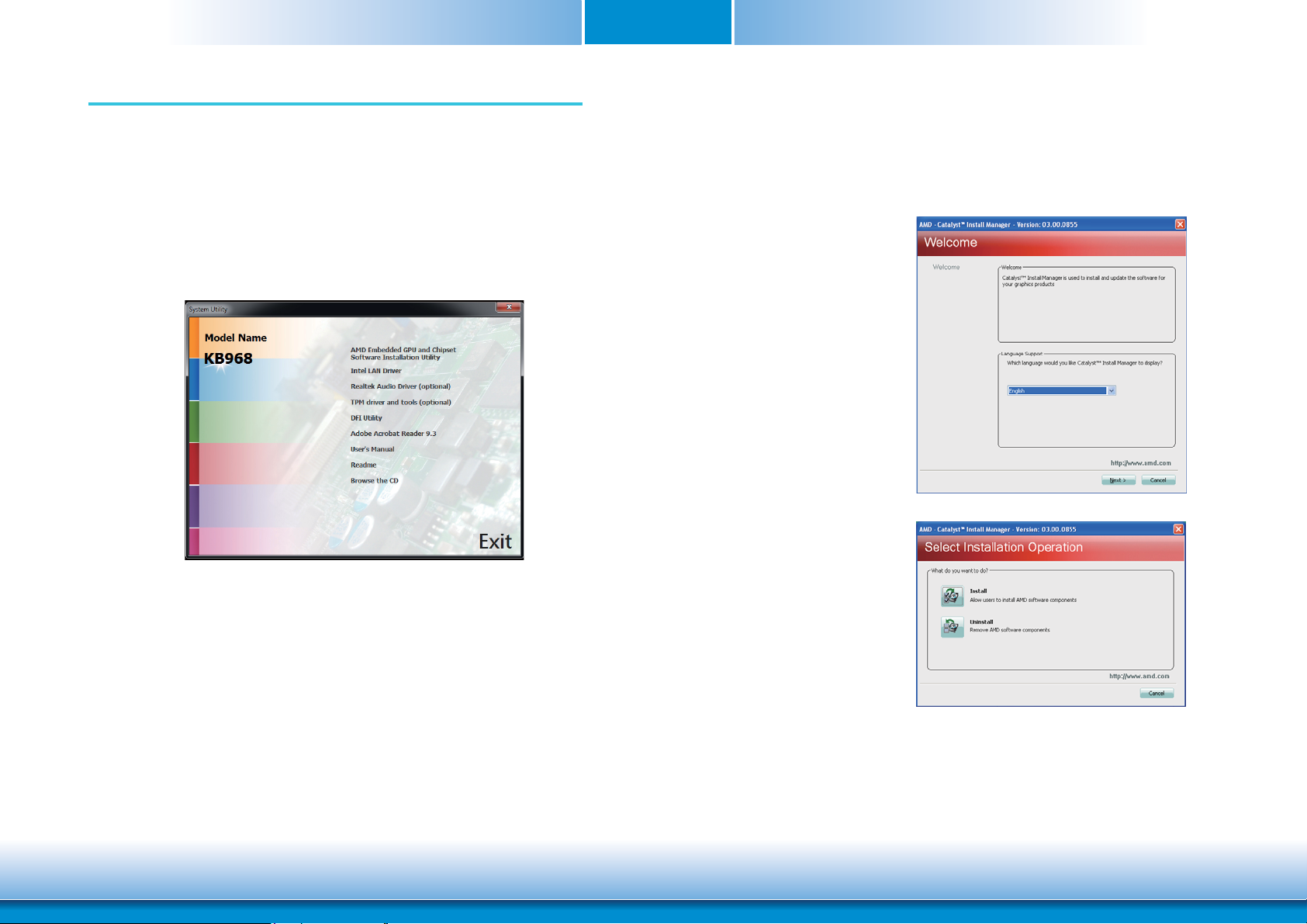
Chapter 5 - Supported Software
The CD that came with the system board contains drivers, utilities and software applications
required to enhance the performance of the system board.
Chapter 5
AMD Embedded GPU and Chipset Software Installation
Utility
Insert the CD into a CD-ROM drive. The autorun screen (Mainboard Utility CD) will appear. If
after inserting the CD, “Autorun” did not automatically start (which is, the Mainboard Utility
CD screen did not appear), please go directly to the root directory of the CD and double-click
“Setup”.
For Windows 7/8
To install the driver, click “AMD Embedded GPU and Chipset Software Installation Utility” on the
main menu.
1. Under the Language Support
section, select the language you
would like the installation to
display and then click Next.
2. Click Install to begin the
installation.
50
www.dfi .comChapter 5 Supported Software
Page 51
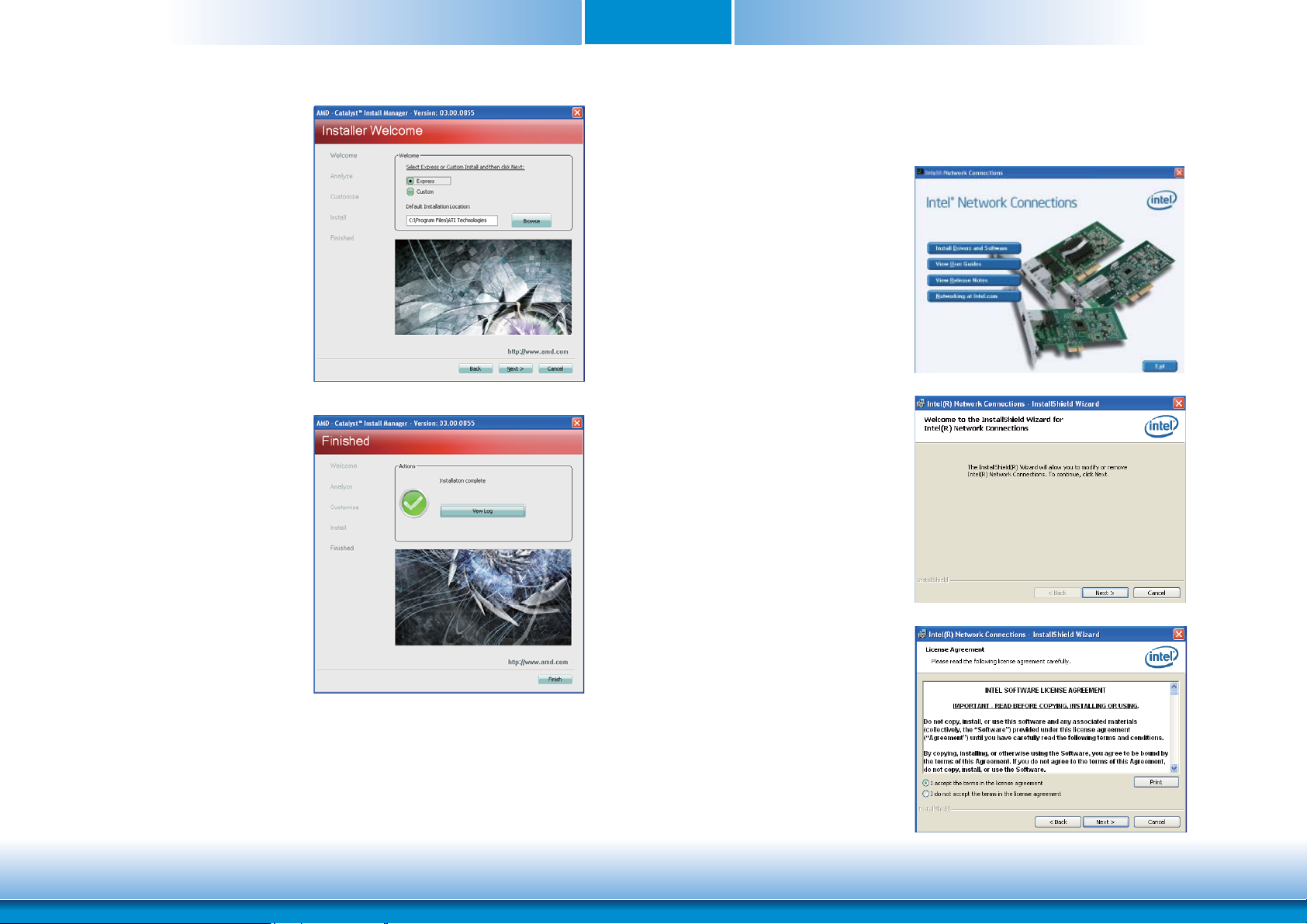
Chapter 5
3. Click Express and then click
Next.
4. After completing installation,
click Finish.
Intel LAN Driver
To install the driver, click “Intel LAN Drivers” on the main menu.
1. Setup is ready to install the driver.
Click Install Drivers and Sofeware.
2. Setup is now ready to install the
LAN driver. Click Next.
3. Click “I accept the terms in the license agreement” then click Next
51
.
www.dfi .comChapter 5 Supported Software
Page 52
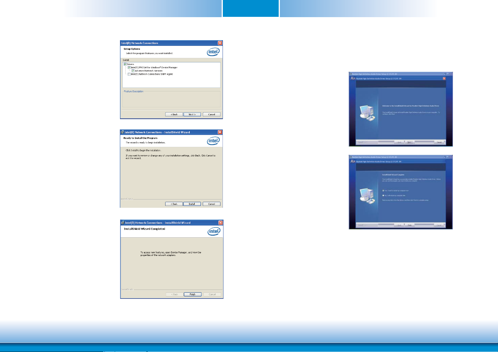
Chapter 5
4. Select the program featuers you
want installed then click Next.
5. Click Install to begin the installation.
Realtek Audio Driver (optional)
To install the driver, click “Realtek Audio Driver (optional)” on the main menu.
1. Setup is now ready to install the
audio driver. Click Next.
2. Follow the remainder of the steps
on the screen; clicking “Next”
each time you finish a step.
3. Click “Yes, I want to restart my
computer now” then click Finish.
Restarting the system will allow the
new software installation to take
effect.
6. After completing installation,
click Finish.
52
www.dfi .comChapter 5 Supported Software
Page 53
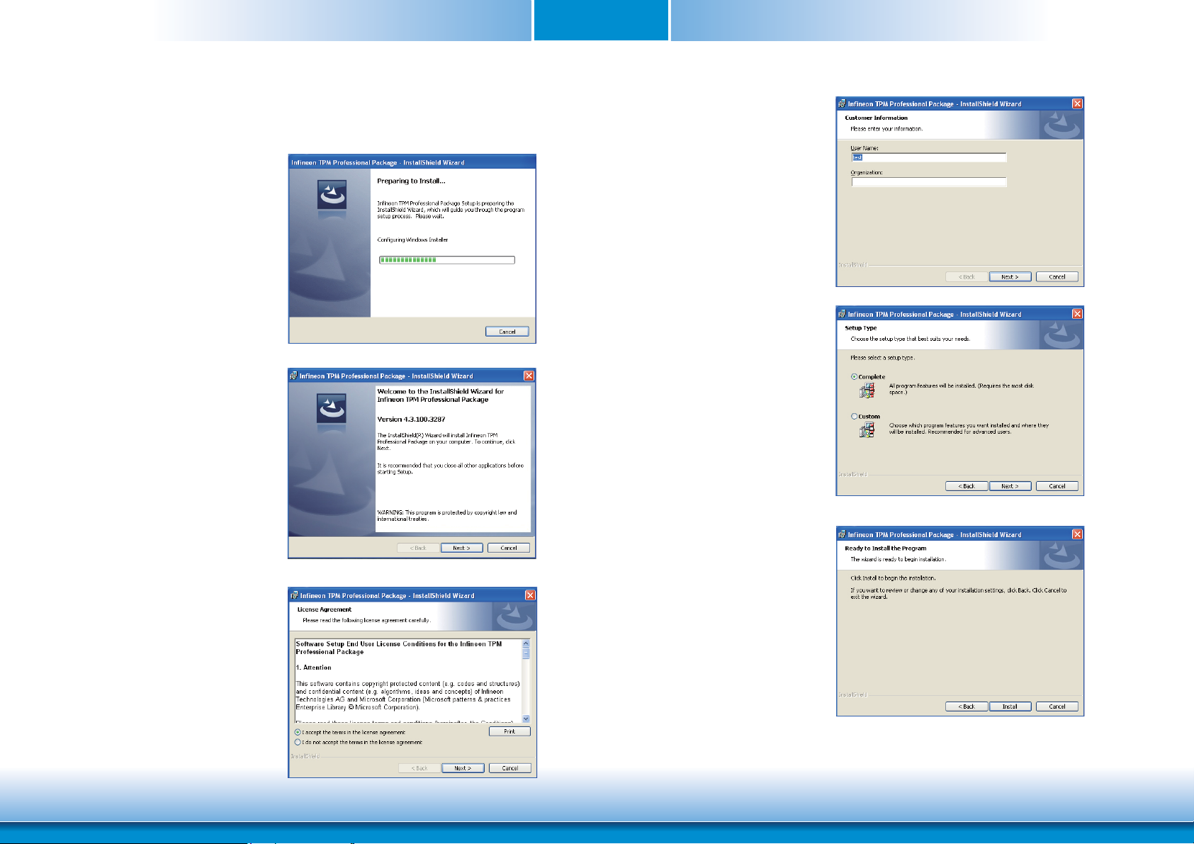
Chapter 5
TPM Driver and Tools (optional)
To install the driver, click “TPM driver and tools (optional)” on the main menu.
1. The setup program is preparing
to install the driver.
2. The setup program is now ready
to install the utility. Click Next.
4. Enter the necessary information
and then click Next.
5. Select a setup type and then click
Next.
3. Click “I accept the terms in the
license agreement” and then
click “Next”.
6. Click Install.
53
www.dfi .comChapter 5 Supported Software
Page 54
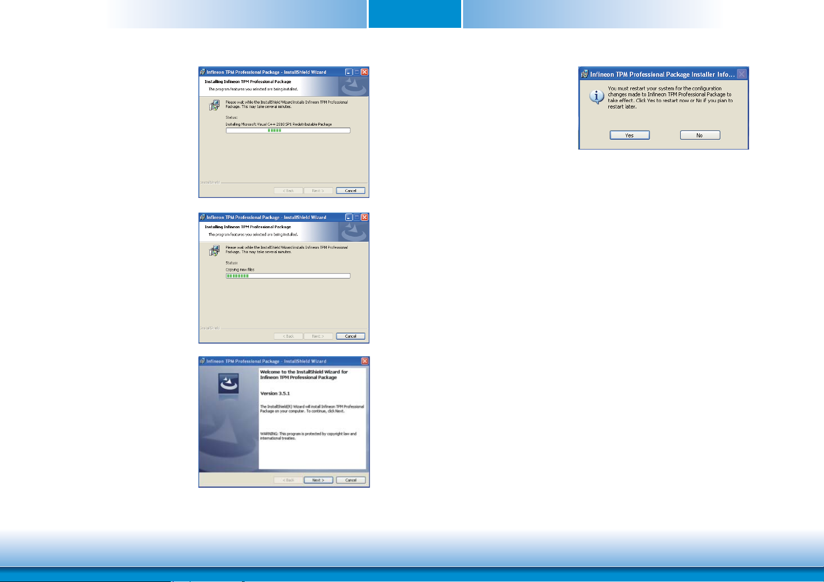
Chapter 5
7. TPM requires installing the Microsoft Visual C++ package prior to
installing the utility. Click Install.
8. The setup program is currently
installing the Microsoft Visual
C++ package.
10. Click “Yes“ to restart your system.
9. Click Finish.
54
www.dfi .comChapter 5 Supported Software
Page 55
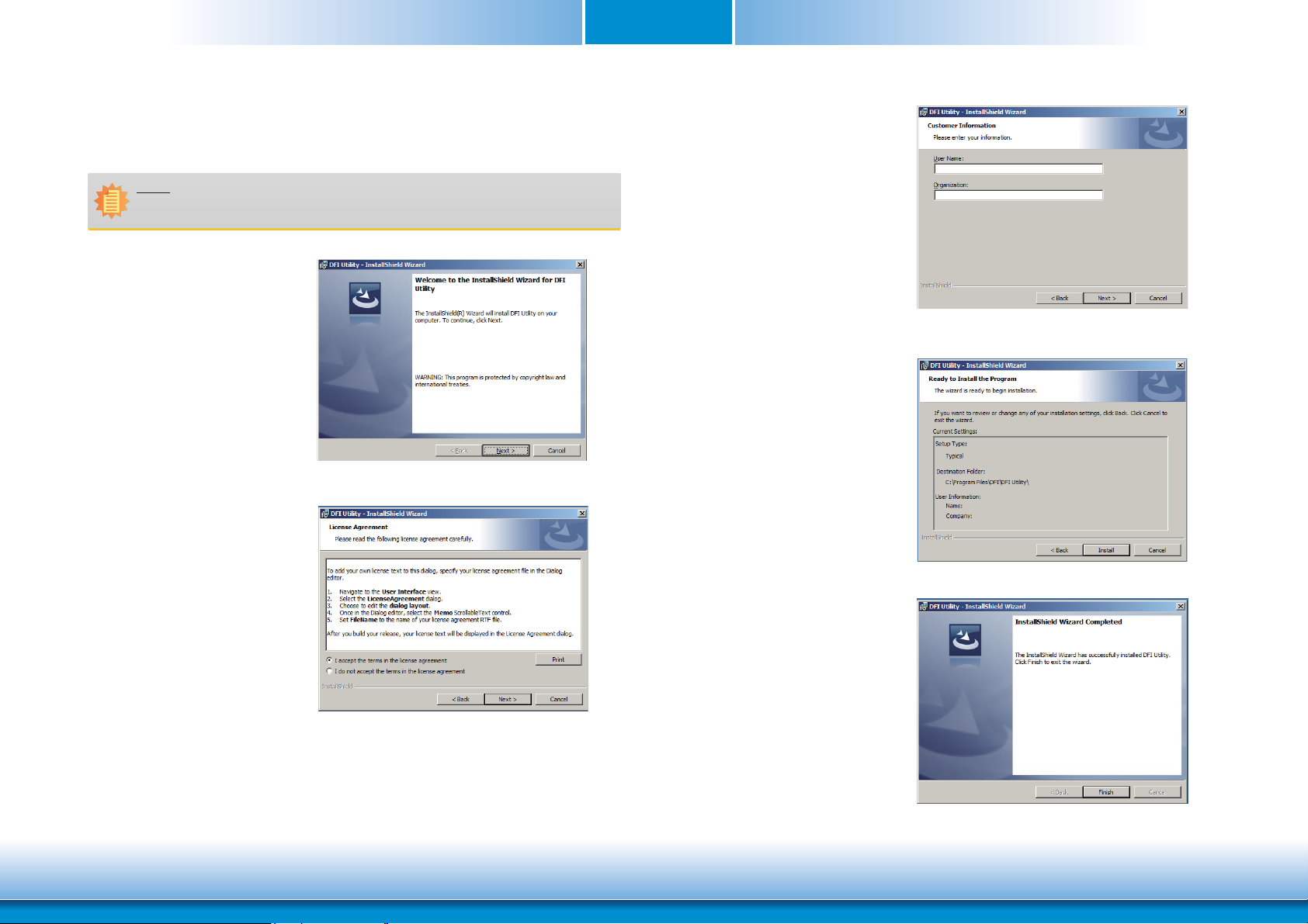
Chapter 5
DFI Utility
DFI Utility provides information about the board, HW Health, Watchdog, DIO, and Backlight. To
access the utility, click “DFI Utility” on the main menu.
Note:
If you are using Windows 7, you need to access the operating system as an administrator to be able to install the utility.
1. Setup is ready to install the DFI
Utility drifer. Click “Next”.
2. Click “I accept the terms in the
license agreement” then click
.
“Next”
3. Enter “User Name” and “Organization” information then click
.
“Next”
4. Click Install to begin the installation.
5. After completing installation,
click Finish.
55
www.dfi .comChapter 5 Supported Software
Page 56
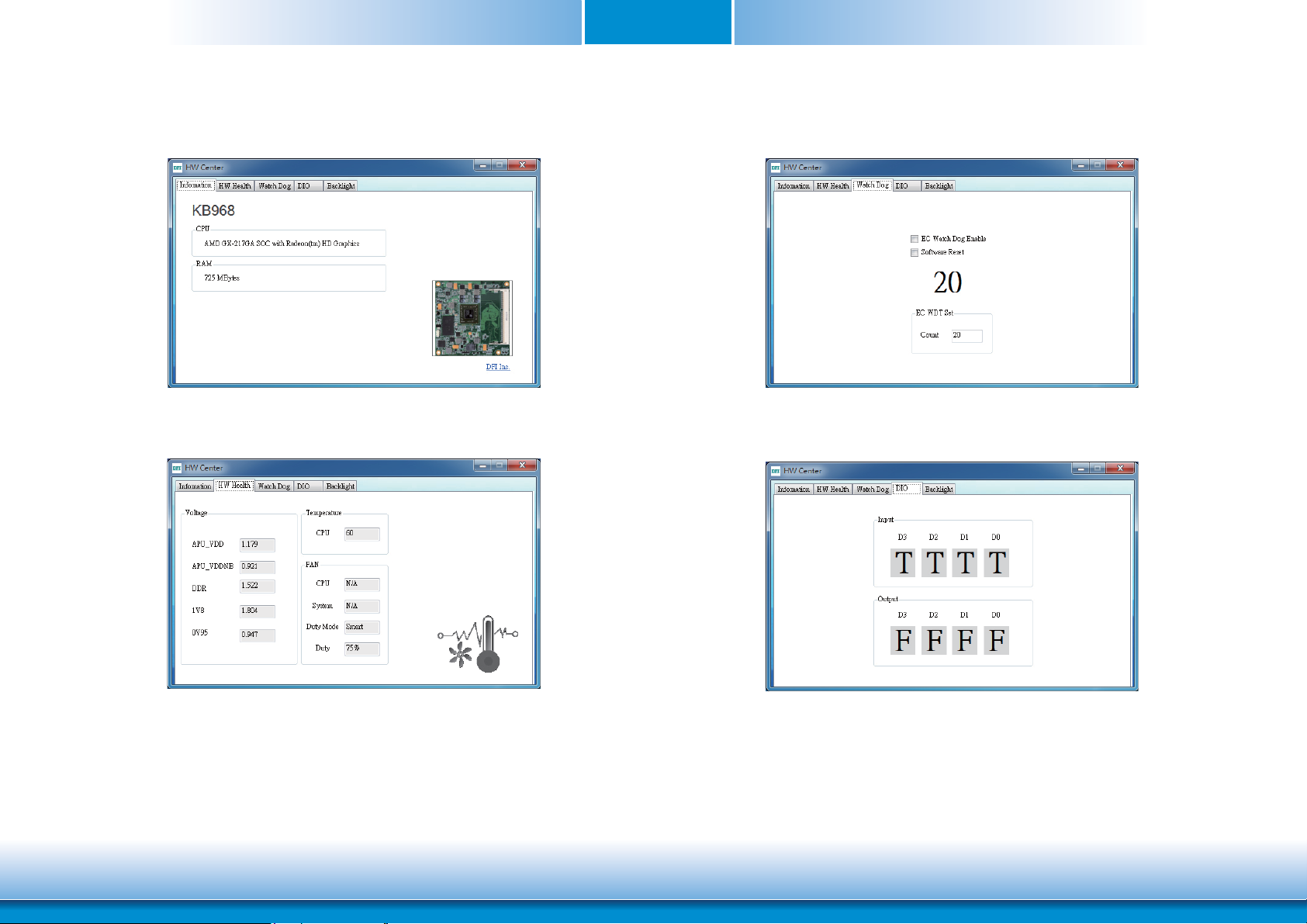
The DFI Utility icon will appear on the desktop. Double-click the icon to open the utility.
Chapter 5
Information
HW Health
WatchDog
DIO
56
www.dfi .comChapter 5 Supported Software
Page 57

Backlight
Chapter 5
Adobe Acrobat Reader 9.3
To install the reader, click “Adobe Acrobat Reader 9.3” on the main menu.
1. Click Next to install or click
Change Destination Folder to
select another folder.
2. Click Install to begin installation.
3. Click Finish to exit installation.
57
www.dfi .comChapter 5 Supported Software
Page 58

Chapter 6 - GPIO Programming Guide
Function Description
Get_EC_Data (unsigned char ucData): Read a Byte data from EC.
Write_EC_Data (unsigned char ucData, unsigned char Data): Write a Byte data to EC.
Sample Code
GPIO Input Process
EC_DIO_Read_Input()
{
BYTE Data;
//Pin0-3 Input Mode
Data = Get_EC_Data(0xBA);
Data |= 0x80;
Write_EC_Data(0xBA, Data);
while(((Get_EC_Data(0xBA) >> 7)&0x01))
{
Data = Get_EC_Data(0xBA);
}
Chapter 6
Return Data ;
}
GPIO Output Process
EC_DIO_Write_Output(unsigned char udata)
{
//Pin4-7 Output Mode
udata <<= 4;
udata |= 0x01;
Write_EC_Data(0xBB, udata);
return 0;
EC_DIO_Read_Output()
{
BYTE Data;
//Pin4-7 Output Mode
Write_EC_Data(0xBB, 0x02);
Delay;
Data = Get_EC_Data(0xBB);
Data >>= 4;
Return Data ;
}
58
www.dfi .comChapter 6 GPIO Programming Guide
Page 59

Appendix A
Appendix A - NLITE and AHCI Installation Guide
nLite
nLite is an application program that allows you to customize your XP installation disc by
integrating the RAID/AHCI drivers into the disc. By using nLite, the F6 function key usually
required during installation is no longer needed.
Note:
The installation steps below are based on nLite version 1.4.9. Installation procedures
may slightly vary if you’re using another version of the program.
1. Download the program from nLite’s offical website.
http://www.nliteos.com/download.html
2. Install nLite.
4. Insert the XP installation disc
into an optical drive.
5. Launch nLite. The Welcome
screen will appear. Click
Next.
Important:
Due to it’s coding with Visual.Net, you may need to first install .NET Framework prior
to installing nLite.
3. Download relevant RAID/AHCI driver files from Intel’s website. The drivers you choose will
depend on the operating system and chipset used by your computer.
The downloaded driver files
should include iaahci.cat,
iaAHCI.inf, iastor.cat, iaStor.
inf, IaStor.sys, license.txt and
TXTSETUP.OEM.
6. Click Next to temporarily
save the Windows installation files to the designated
default folder.
If you want to save them in
another folder, click Browse,
select the folder and then click
Next.
59
www.dfi .comAppendix A NLITE and AHCI Installation Guide
Page 60
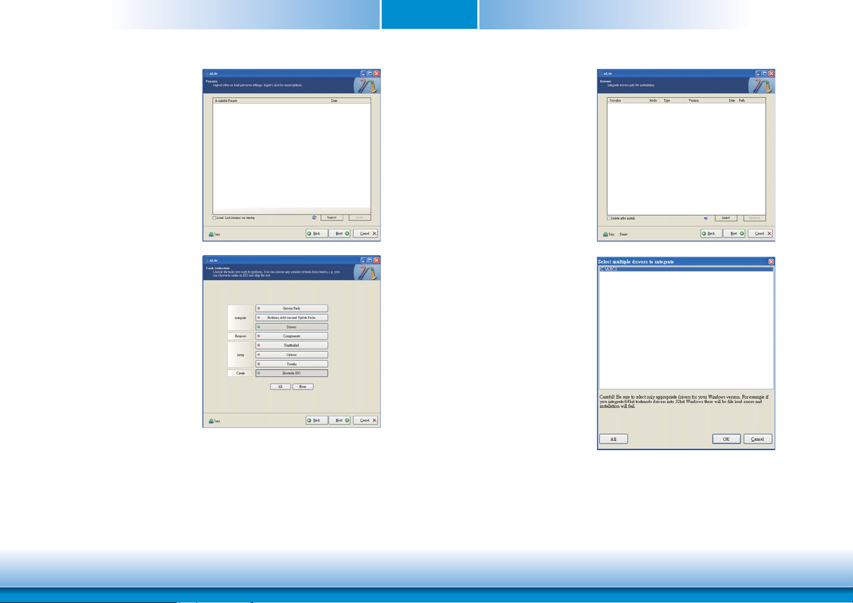
Appendix A
7. Click Next.
8. In the Task Selection dialog
box, click Drivers and
Bootable ISO. Click Next.
9. Click Insert and then select
Multiple driver folder to
select the drivers you will
integrate. Click Next.
10. Select only the drivers ap-
propriate for the Windows
version that you are using
and then click OK.
Integrating 64-bit drivers into
32-bit Windows or vice versa
will cause file load errors and
failed installation.
60
www.dfi .comAppendix A NLITE and AHCI Installation Guide
Page 61
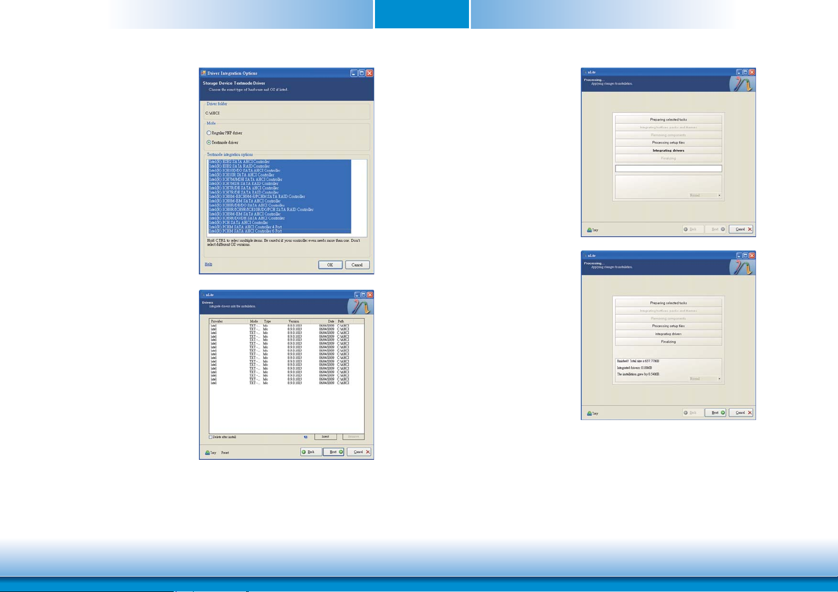
Appendix A
11. If you are uncertain of the
southbridge chip used on
your motherboard, select all
RAID/AHCI controllers and
then click OK
12. Click Next.
.
13. The program is currently
integrating the drivers and
applying changes to the
installation.
14. When the program is finished applying the changes,
click Next.
61
www.dfi .comAppendix A NLITE and AHCI Installation Guide
Page 62
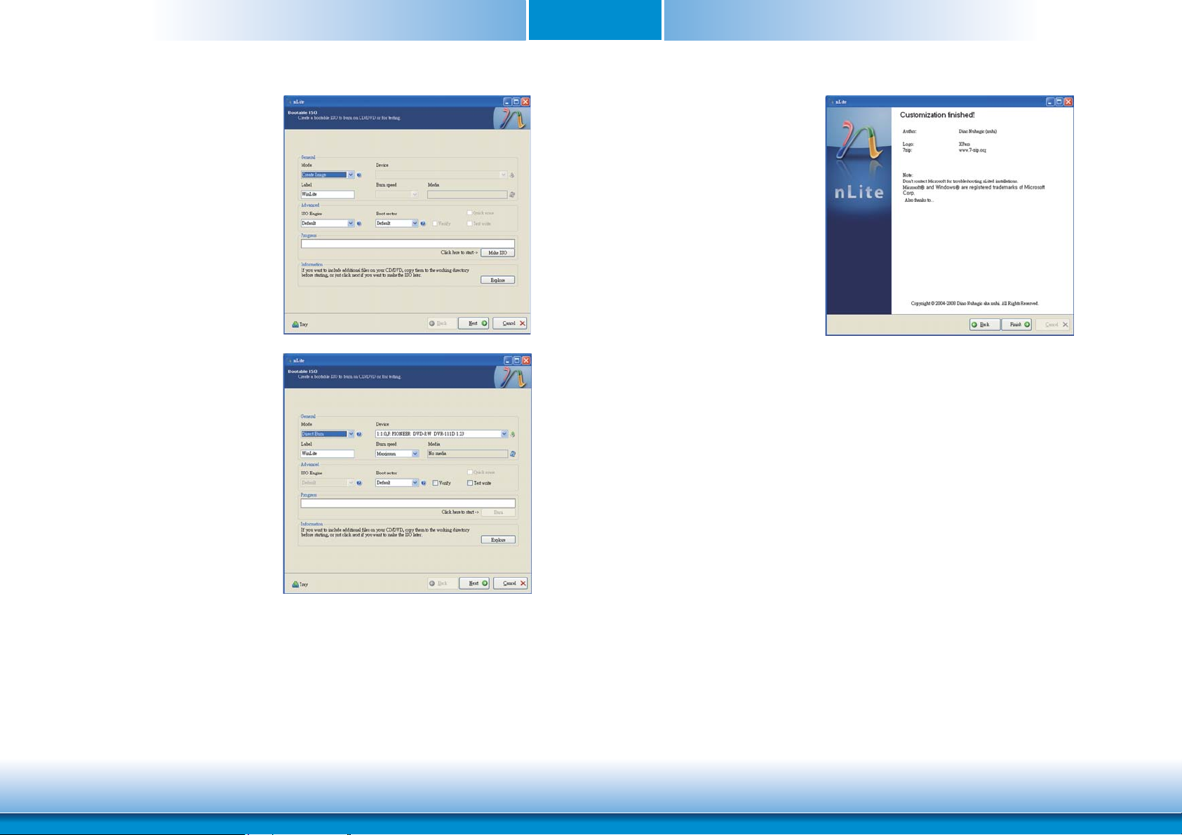
Appendix A
15. To create an image, select the
Create Image mode under the
General section and then click
Next.
16. Or you can choose to burn it
directly to a disc by selecting
the Direct Burn mode under
the General section.
Select the optical device and all
other necessary settings and then
click Next
.
17. You have finished customizing
the Windows XP installation disc.
Click Finish.
Enter the BIOS utility to configure
the SATA controller to RAID/AHCI.
You can now install Windows XP.
62
www.dfi .comAppendix A NLITE and AHCI Installation Guide
Page 63
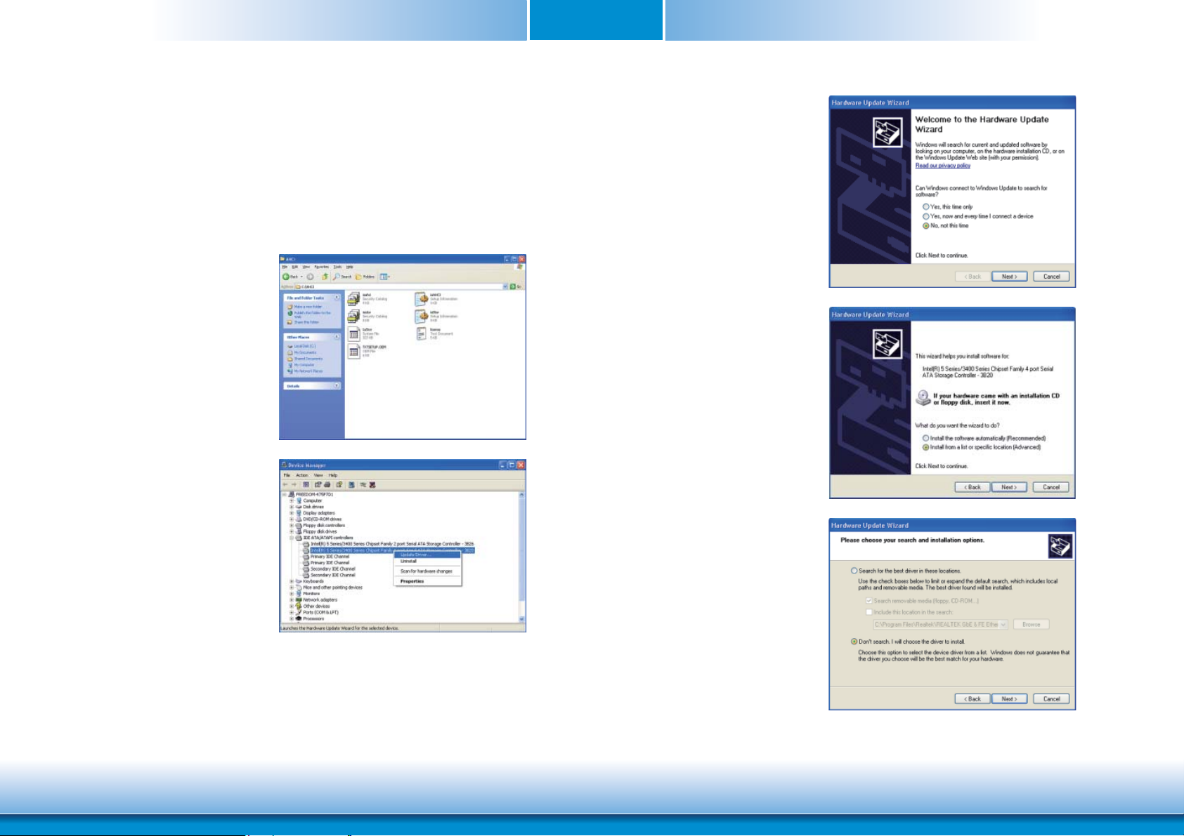
Appendix A
AHCI
The installation steps below will guide you in configuring your SATA drive to AHCI
mode.
1. Enter the BIOS utility and configure the SATA controller to IDE mode.
2. Install Windows XP but do not press F6.
3. Download relevant RAID/AHCI driver files supported by the motherboard chipset from Intel’s website.
Transfer the downloaded driver
files to C:\AHCI.
4. Open Device Manager and
right click on one of the
Intel Serial ATA Storage Controllers, then select Update
Driver.
If the controller you selected
did not work, try selecting
another one.
5. In the Hardware Update Wizard
dialog box, select “No, not this
time” then click Next.
6. Select “Install from a list or
specific location (Advanced)” and
then click Next.
7. Select “Don’t search. I will choose
the driver to install” and then click
.
Next
63
www.dfi .comAppendix A NLITE and AHCI Installation Guide
Page 64
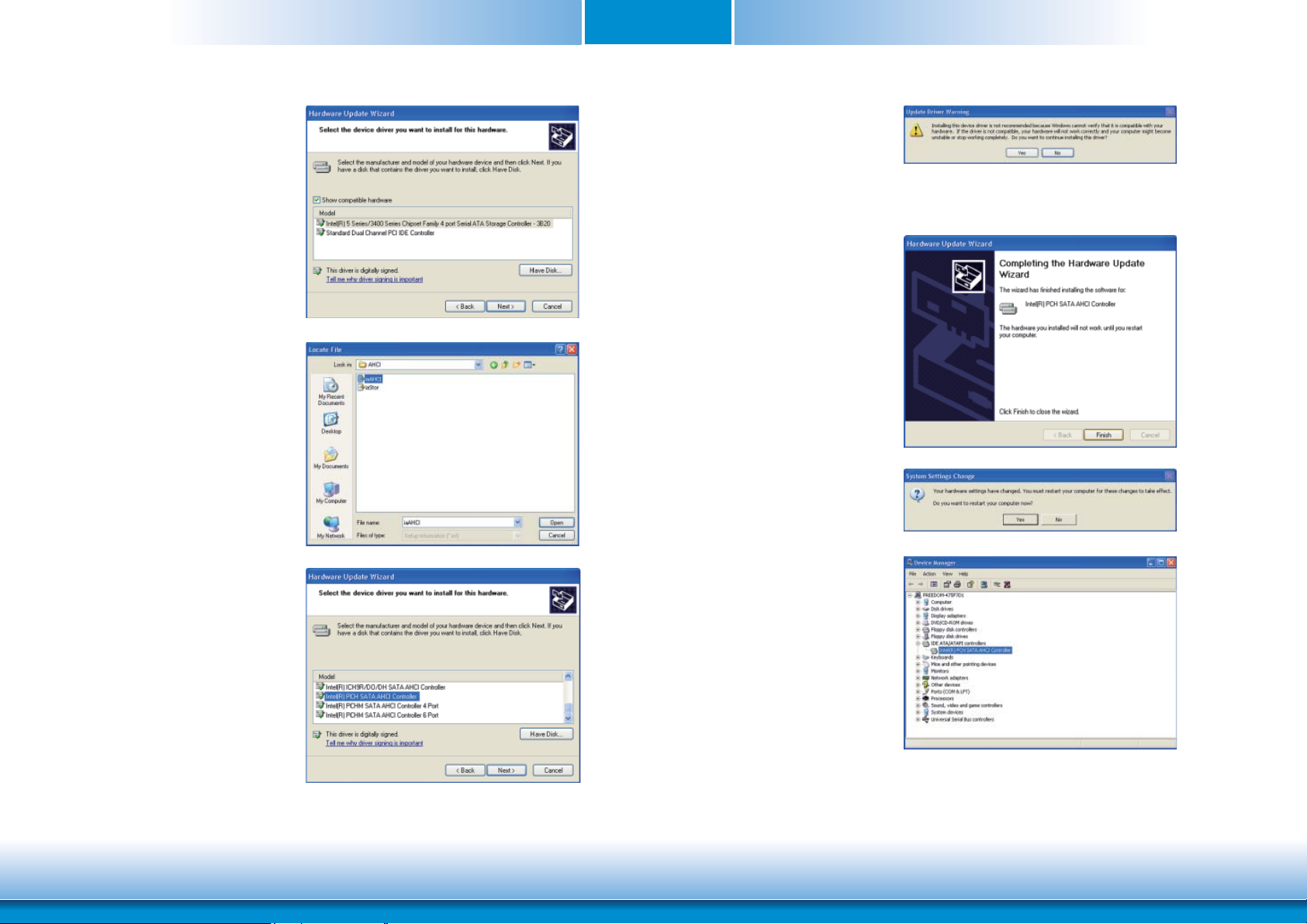
Appendix A
8. Click “Have Disk”.
9. Select C:\AHCI\iaAHCI.inf
and then click Open.
11. A warning message appeared
because the selected SATA
controller did not match your
hardware device.
Ignore the warning and click Yes to
proceed.
12. Click Finish.
13. The system’s settings have
been changed. Windows XP
requires that you restart the
computer. Click Yes.
10. Select the appropriate AHCI
Controller of your hardware
device and then click Next.
14. Enter the BIOS utility and
modify the SATA controller
from IDE to AHCI. By doing
so, Windows will work normally
with the SATA controller that is
in AHCI mode.
64
www.dfi .comAppendix A NLITE and AHCI Installation Guide
Page 65

Appendix B - Watchdog Sample Code
Appendix B
#include <stdio.h>
//-------------------------------------------------------------#defi ne EC_EnablePort 0x66
#defi ne EC_DataPort 0x62
//-------------------------------------------------------------void WriteEC(char,int);
void SetWDTime(int,int);
int GetWDTime(void);
//-------------------------------------------------------------main()
{
unsigned int countdown;
unsigned int input,count_h,count_l;
printf("Input WD Time: ");
scanf("%d",&input);
printf("\n");
count_h=input>>8;
count_l=input&0x00FF;
SetWDTime(count_h,count_l);
while(1)
{
countdown = GetWDTime();
delay(100);
printf("\rTime Remaining: %d ",countdown);
}
}
//-------------------------------------------------------------void SetWDTime(int count_H,int count_L)
{
//Set Count
WriteEC(0xB7,count_H); //High Byte
WriteEC(0xB8,count_L); //Low Byte
//Enable Watch Dog Timer
WriteEC(0xB4,0x02);
}
//--------------------------------------------------------------
int GetWDTime(void)
{
int sum,data_h,data_l;
//Select EC Read Type
outportb(EC_EnablePort,0x80);
delay(5);
//Get Remaining Count High Byte
outportb(EC_DataPort,0xF6);
delay(5);
data_h=inportb(EC_DataPort);
delay(5);
//Select EC Read Type
outportb(EC_EnablePort,0x80);
delay(5);
//Get Remaining Count Low Byte
outportb(EC_DataPort,0xF7);
delay(5);
data_l=inportb(EC_DataPort);
delay(5);
data_h<<=8;
data_h&=0xFF00;
sum=data_h|data_l;
return sum;
}
//-------------------------------------------------------------void WriteEC(char EC_Addr, int data)
{
//Select EC Write Type
outportb(EC_EnablePort,0x81);
delay(5);
outportb(EC_DataPort,EC_Addr);
delay(5);
outportb(EC_DataPort,data);
delay(5);
}
//--------------------------------------------------------------
65
www.dfi .comAppendix B Watchdog Sample Code
Page 66
Appendix C
Appendix C - System Error Message
When the BIOS encounters an error that requires the user to correct something, either a beep
code will sound or a message will be displayed in a box in the middle of the screen and the
message, PRESS F1 TO CONTINUE, CTRL-ALT-ESC or DEL TO ENTER SETUP, will be shown in
the information box at the bottom. Enter Setup to correct the error.
Error Messages
One or more of the following messages may be displayed if the BIOS detects an error during
the POST. This list indicates the error messages for all Awards BIOSes:
CMOS BATTERY HAS FAILED
The CMOS battery is no longer functional. It should be replaced.
Important:
Danger of explosion if battery incorrectly replaced. Replace only with the same or
equivalent type recommended by the manufacturer. Dispose of used batteries according to the battery manufacturer’s instructions.
CMOS CHECKSUM ERROR
Checksum of CMOS is incorrect. This can indicate that CMOS has become corrupt. This error
may have been caused by a weak battery. Check the battery and replace if necessary.
DISPLAY SWITCH IS SET INCORRECTLY
The display switch on the motherboard can be set to either monochrome or color. This indicates the switch is set to a different setting than indicated in Setup. Determine which setting
is correct, either turn off the system and change the jumper or enter Setup and change the
VIDEO selection.
66
www.dfi .comAppendix C System Error Message
Page 67

Appendix D - Troubleshooting
Appendix D
The picture seems to be constantly moving.
Troubleshooting Checklist
This chapter of the manual is designed to help you with problems that you may encounter
with your personal computer. To efficiently troubleshoot your system, treat each problem individually. This is to ensure an accurate diagnosis of the problem in case a problem has multiple
causes.
Some of the most common things to check when you encounter problems while using your
system are listed below.
1. The power switch of each peripheral device is turned on.
2. All cables and power cords are tightly connected.
3. The electrical outlet to which your peripheral devices are connected is working. Test the
outlet by plugging in a lamp or other electrical device.
4. The monitor is turned on.
5. The display’s brightness and contrast controls are adjusted properly.
6. All add-in boards in the expansion slots are seated securely.
7. Any add-in board you have installed is designed for your system and is set up correctly.
Monitor/Display
If the display screen remains dark after the system is turned on:
1. Make sure that the monitor’s power switch is on.
2. Check that one end of the monitor’s power cord is properly attached to the monitor and the
other end is plugged into a working AC outlet. If necessary, try another outlet.
1. The monitor has lost its vertical sync. Adjust the monitor’s vertical sync.
2. Move away any objects, such as another monitor or fan, that may be creating a magnetic
field around the display.
3. Make sure your video card’s output frequencies are supported by this monitor.
The screen seems to be constantly wavering.
1. If the monitor is close to another monitor, the adjacent monitor may need to be turned off.
Fluorescent lights adjacent to the monitor may also cause screen wavering.
Power Supply
When the computer is turned on, nothing happens.
1. Check that one end of the AC power cord is plugged into a live outlet and the other end
properly plugged into the back of the system.
2. Make sure that the voltage selection switch on the back panel is set for the correct type of
voltage you are using.
3. The power cord may have a “short” or “open”. Inspect the cord and install a new one if
necessary.
3. Check that the video input cable is properly attached to the monitor and the system’s
display adapter.
4. Adjust the brightness of the display by turning the monitor’s brightness control knob
.
67
www.dfi .comAppendix D Troubleshooting
Page 68

Appendix D
Hard Drive
Hard disk failure.
1. Make sure the correct drive type for the hard disk drive has been entered in the BIOS.
2. If the system is configured with two hard drives, make sure the bootable (first) hard drive
is configured as Master and the second hard drive is configured as Slave. The master hard
drive must have an active/bootable partition.
Excessively long formatting period.
If your hard drive takes an excessively long period of time to format, it is likely a cable connection problem. However, if your hard drive has a large capacity, it will take a longer time to
format.
Serial Port
The serial device (modem, printer) doesn’t output anything or is outputting garbled
characters.
1. Make sure that the serial device’s power is turned on and that the device is on-line.
2. Verify that the device is plugged into the correct serial port on the rear of the computer.
3. Verify that the attached serial device works by attaching it to a serial port that is working and configured correctly. If the serial device does not work, either the cable or the serial
device has a problem. If the serial device works, the problem may be due to the onboard I/O
or the address setting.
4. Make sure the COM settings and I/O address are configured correctly.
System Board
1. Make sure the add-in card is seated securely in the expansion slot. If the add-in card is
loose, power off the system, re-install the card and power up the system.
2. Check the jumper settings to ensure that the jumpers are properly set.
3. Verify that all memory modules are seated securely into the memory sockets.
4. Make sure the memory modules are in the correct locations.
5. If the board fails to function, place the board on a flat surface and seat all socketed compo-
nents. Gently press each component into the socket.
6. If you made changes to the BIOS settings, re-enter setup and load the BIOS defaults.
Keyboard
Nothing happens when a key on the keyboard was pressed.
1. Make sure the keyboard is properly connected.
2. Make sure there are no objects resting on the keyboard and that no keys are pressed during the booting process.
68
www.dfi .comAppendix D Troubleshooting
 Loading...