

Page 1

www.dfi .comChapter 1 Introduction
1
COM333-I
COM Express Carrier Board
User’s Manual
A47100832
Preliminary
Version
Page 2

www.dfi .comChapter 1 Introduction
2
Copyright
This publication contains information that is protected by copyright. No part of it may be reproduced in any form or by any means or used to make any transformation/adaptation without
the prior written permission from the copyright holders.
This publication is provided for informational purposes only. The manufacturer makes no
representations or warranties with respect to the contents or use of this manual and specifically disclaims any express or implied warranties of merchantability or fitness for any particular
purpose. The user will assume the entire risk of the use or the results of the use of this document. Further, the manufacturer reserves the right to revise this publication and make changes
to its contents at any time, without obligation to notify any person or entity of such revisions
or changes.
Changes after the publication’s first release will be based on the product’s revision. The website
will always provide the most updated information.
© 2018. All Rights Reserved.
Trademarks
Product names or trademarks appearing in this manual are for identification purpose only and
are the properties of the respective owners.
FCC and DOC Statement on Class B
This equipment has been tested and found to comply with the limits for a Class B digital
device, pursuant to Part 15 of the FCC rules. These limits are designed to provide reasonable protection against harmful interference when the equipment is operated in a residential
installation. This equipment generates, uses and can radiate radio frequency energy and, if not
installed and used in accordance with the instruction manual, may cause harmful interference
to radio communications. However, there is no guarantee that interference will not occur in a
particular installation. If this equipment does cause harmful interference to radio or television
reception, which can be determined by turning the equipment off and on, the user is encouraged to try to correct the interference by one or more of the following measures:
• Reorient or relocate the receiving antenna.
• Increase the separation between the equipment and the receiver.
• Connect the equipment into an outlet on a circuit different from that to which the receiver
is connected.
• Consult the dealer or an experienced radio TV technician for help.
Notice:
1. The changes or modifications not expressly approved by the party responsible for compliance could void the user’s authority to operate the equipment.
2. Shielded interface cables must be used in order to comply with the emission limits.
Page 3

www.dfi .comChapter 1 Introduction
3
Table of Contents
Copyright ........................................................................................................... ..2
Trademarks ........................................................................................................2
FCC and DOC Statement on Class B ..................................................... 2
Warranty .............................................................................................................. 4
Static Electricity Precautions ...................................................................... 4
Safety Measures ..............................................................................................4
About the Package .........................................................................................5
Optional Items..................................................................................................5
Before Using the System Board ............................................................... 5
Chapter 1 - Introduction .............................................................................6
Specifications ................................................................................................6
Chapter 2 - Hardware Installation ................................................ 7
Board Layout .................................................................................................7
Function Test Jumper .................................................................................8
Battery Low Indicator ...................................................................................8
Jumper Settings ...........................................................................................8
USB Power Select .........................................................................................8
USB 2.0 Port 3 Select ...................................................................................9
10G PHY Capability Select ............................................................................. 9
PCIe Lane Select ........................................................................................ 10
PCIe Lane 12 Select ...................................................................................10
TPM_PP on CB Select .................................................................................11
ESPI- Enable Select .................................................................................... 11
BIOS Boot Location Select........................................................................... 12
PIN 0~3 DIO Output/Input Select ............................................................... 12
VCC5_IN Power Select ................................................................................13
ATX/AT Mode Select (Power_OK) ................................................................. 13
PS_ON Select ............................................................................................. 14
Clear CMOS ................................................................................................ 14
BMC UART1 Port Mode Select ..................................................................... 15
BMC UART1 Driver’s/Receiver’s Power Rail Select ......................................... 15
BMC SPI1 Interface Mode Select ................................................................. 16
BMC 2nd Boot Watchdog Timer Select ......................................................... 16
BMC MAC#1 Interface Type Select ..............................................................17
BMC VGA Select .........................................................................................17
Rear Panel I/O Ports .................................................................................18
Graphics Interface ...................................................................................... 18
COM (Serial) Ports ...................................................................................... 19
LAN Ports ................................................................................................... 20
USB Ports ................................................................................................... 20
I/O Connectors ........................................................................................... 21
LPC Connector ............................................................................................ 21
Digital I/O Connector .................................................................................. 21
SATA (Serial ATA) Connectors ...................................................................... 22
Cooling Fan Connectors...............................................................................22
I
2
C Header ................................................................................................. 23
SMBus Header ............................................................................................ 23
Power Connectors ....................................................................................... 24
Battery ....................................................................................................... 24
Front Panel Connector ................................................................................25
Expansion Slots .......................................................................................... 26
COM Express Connectors ............................................................................26
SDIO (Optional) .......................................................................................... 30
Switches .................................................................................................... 30
LEDs .......................................................................................................... 31
Inphi Configure Pin-Plug ............................................................................. 31
eSPI Female Header ...................................................................................32
Page 4
www.dfi .comChapter 1 Introduction
4
Warranty
1. Warranty does not cover damages or failures that arised from misuse of the product,
inability to use the product, unauthorized replacement or alteration of components and
product specifications.
2. The warranty is void if the product has been subjected to physical abuse, improper installation, modification, accidents or unauthorized repair of the product.
3. Unless otherwise instructed in this user’s manual, the user may not, under any circumstances, attempt to perform service, adjustments or repairs on the product, whether in or
out of warranty. It must be returned to the purchase point, factory or authorized service
agency for all such work.
4. We will not be liable for any indirect, special, incidental or consequencial damages to the
product that has been modified or altered.
Static Electricity Precautions
It is quite easy to inadvertently damage your PC, system board, components or devices even
before installing them in your system unit. Static electrical discharge can damage computer
components without causing any signs of physical damage. You must take extra care in handling them to ensure against electrostatic build-up.
1. To prevent electrostatic build-up, leave the system board in its anti-static bag until you are
ready to install it.
2. Wear an antistatic wrist strap.
3. Do all preparation work on a static-free surface.
4. Hold the device only by its edges. Be careful not to touch any of the components, contacts
or connections.
5. Avoid touching the pins or contacts on all modules and connectors. Hold modules or connectors by their ends.
Safety Measures
To avoid damage to the system:
• Use the correct AC input voltage range.
To reduce the risk of electric shock:
• Unplug the power cord before removing the system chassis cover for installation or servicing. After installation or servicing, cover the system chassis before plugging the power
cord.
Battery:
• Danger of explosion if battery incorrectly replaced.
• Replace only with the same or equivalent type recommend by the manufacturer.
• Dispose of used batteries according to local ordinance.
Important:
Electrostatic discharge (ESD) can damage your processor, disk drive and other components. Perform the upgrade instruction procedures described at an ESD workstation only. If such a station is not available, you can provide some ESD protection by
wearing an antistatic wrist strap and attaching it to a metal part of the system chassis. If a wrist strap is unavailable, establish and maintain contact with the system
chassis throughout any procedures requiring ESD protection.
Page 5

www.dfi .comChapter 1 Introduction
5
About the Package
The package contains the following items. If any of these items are missing or damaged,
please contact your dealer or sales representative for assistance.
• One COM333-I board
• One Serial ATA data cable (Length: 500mm)
Optional Items
• Serial ATA data cable (Length: 500mm)
• LPC EXT-RS232 module (4 x RS232 ports)
• LPC EXT-RS485 module (4 x RS485 ports)
• I/O shield
• Standoff (M2.5*12) (for compact size module)
The board and accessories in the package may not come similar to the information listed
above. This may differ in accordance with the sales region or models in which it was sold. For
more information about the standard package in your region, please contact your dealer or
sales representative.
Before Using the System Board
Before using the system board, prepare basic system components.
If you are installing the system board in a new system, you will need at least the following
internal components.
• Memory module
• Storage devices such as hard disk drive, etc.
You will also need external system peripherals you intend to use which will normally include at
least a keyboard, a mouse and a video display monitor.
Page 6
www.dfi .comChapter 1 Introduction
6
ENVIRONMENT
Temperature Operating: 0 to 60°C
Storage: -40 to 85°C
Humidity Operating: 5 to 90% RH
Storage: 5 to 90% RH
MTBF TBD
MECHANICAL
Dimensions microATX Form Factor
244mm (9.6") x 244mm (9.6")
Compliance PICMG COM Express
®
R3.0, Type 7
Basic, Compact Modules
Chapter 1 - Introduction
Specifications
Chapter 1
EXPANSION
Interface B1: 2 x PCIe x4 or 1 x PCIe x8 (Gen 3)
B2: 2 x PCIe x4 or 1 x PCIe x8 (Gen 3)
B3: 2 x PCIe x4 or 1 x PCIe x8 (Gen 3)
B4: 2 x PCIe x4 or 1 x PCIe x8 (Gen 3)
REAR I/O
Ethernet 4 x 10GbE LAN (2 x RJ-45, 2 x SFP+) by 10GBASE-KR interface
2 x 1GbE LAN (RJ-45) (one from module; another from BMC for remote management)
USB 4 x USB 3.0/2.0
Serial 1 x RS-232 (DB-9) (supports by BMC which default is debug port and may switch to
normal RS-232)
INTERNAL
I/O
Serial 2 x Serial Interface Connectors (TX/RX) (2.0mm pitch)
SATA 2 x SATA 3.0 (up to 6Gb/s)
DIO 1 x 8-bit DIO (4 input, 4 output)
1 x SDIO (available upon request)
LPC 1 x LPC
SMBus 1 x SMBus
BMC
Features 1. IPMI 2.0
2. Web Browser Support
3. Web Interface
4. iKVM (keyboard, video and mouse)
5. Virtual Media
6. 3rd Party Authentication
7. Firmware Update
8. SMASH/CLP
9. WS-MAN
10. Network Service
Processor AST2500
SDRAM DDR4-2400 1200MHz 8Gb memory down
Display Through BMC to convert VGA signal
VGA: resolution up to 1920 x 1200 x 32bpp (share with SOC 16MB memory)
POWER
Type 12V, 5VSB, VCC_RTC (ATX mode)
12V, VCC_RTC (AT mode)
Connector 4-pin ATX 12V power
24-pin ATX power
RTC Battery CR2032 Coin Cell
Page 7
www.dfi .comChapter 2 Hardware Installation
7
Chapter 2
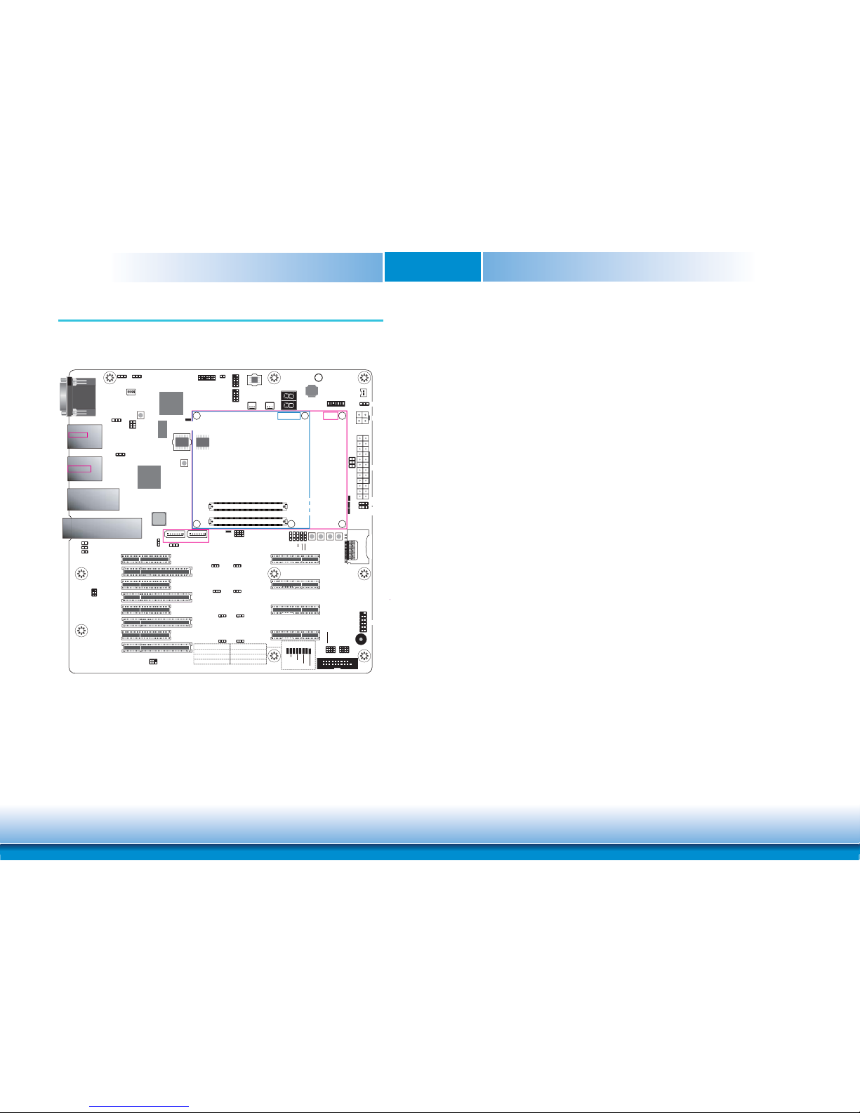
Chapter 2 - Hardware Installation
Board Layout
DDR4
Inphi
CS4227
ASPEED
AST2500
EZX557AT2
COM 1
9
1
2
COM 2
PCIe 8
(PCIe x4)
PCIe 5
(PCIe x4)
PCIe 6
(PCIe x4)
PCIe 7
(PCIe x4)
PCIe 1
(PCIe x8)
PCIe 2
(PCIe x8)
PCIe 3
(PCIe x8)
PCIe 4
(PCIe x8)
PCIe 12 (PCIe x4)
PCIe 10 (PCIe x4)
PCIe 11 (PCIe x4)
PCIe 9 (PCIe x4)
PCIe Lanes 28~31
Select (JP17)
PCIe Lanes 04~07
Select (JP10)
PCIe Lanes 08~11
Select (JP15)
PCIe Lanes 12~15
Select (JP11)
PCIe Lanes 16~19
Select (JP12)
PCIe Lanes 20~23
Select (JP16)
PCIe Lanes 24~27
Select (JP13)
PCIe Lanes 00~03
Select (JP14)
Thermal
Trip LED
PCIe Lane 12
Select (JP18)
Battery Low Indicator (J4)
Microsel0 Select (J18)
BMC VGA Select (J20)
Compact
Basic
SPI Flash BIOS
Buzzer
1G RJ-45 LAN 1
USB 0,1
USB 3.0
10G SFP+ LAN 1,2
1
1
2
19
Digital I/O
1
1
24
ATX Power
13
1
12
11
2
1
1
SATA 1
SATA 3.0
5
1
2
SMBus HDR
+12V Power
VCC5_IN Power
Select (JP26)
12
56
1
1
USB 3.0 Ports 0,1
Power Select
(JP1)
USB 3.0 Ports 2,3
Power Select (JP2)
LC4064ZE
Debug
LED
LPC
Clear CMOS (JP29)
ATX/AT Mode Select
(Power_OK) (JP27)
PS_ON Select (JP28)
Front Panel
System
Fan2
11
System
Fan1
1
1
1
B110
A110
B1
A1
COM Express Connector
D110
C110
D1
C1
COM Express Connector
1G MGMT LAN
USB 2,3
USB 3.0
10G RJ-45 LAN 3,4
1
1
1
5
1
6
2
1
1
21
5
I2C HDR
Battery
1
PIN GPO0~3
DIO Output
(JP24)
PIN GPI0~3
DIO Input
(JP25)
10G PHY CAP 2,3 Select (JP9)
1
SATA 0
BMC UART1 Driver’s/Receiver’s
Power Rail Select (JP31)
BMC UART1 Port Mode Select (JP30)
SPI
TPM
Disable
1
USB 2.0 Port 3
Select (JP4)
1
ON
2
3
4
SW1
1
10
12 3
1
10
12 3
1
10
12
3
BMC AST2500
Chip Level Reset
2
1
13
14
BMC AST2500 SOC
Level Reset
LED20
LED
9
LED10
LED15LED
13
LED12
LED14
LED
11
GPO0 LED (LED12)
GPO3 LED (LED9)
GPO2 LED (LED10)
GPO1 LED (LED11)
GPI0 LED (LED20)
GPI1 LED (LED15)
GPI2 LED (LED14)
GPI3 LED (LED13)
1
1
1
1
1
1
Sleep
Lid
Power
Reset
SDIO
(optional)
111
10G PHY CAP 0,1
Select (JP19)
BIOS Boot Location Select (JP22, JP23)
ESPI- Enable Select (JP21)
TPM_PP on CB Select (JP20)
1
1
BMC UART1
VGA
eSPI Female HDR
9
1
2
BMC 1st SPI Flash
2
1
13
14
1
Inphi
Configure
Pin-Plug
(JP8)
BMC AST2500
Heart Beat LED
Indicator LED for
Non-Type 7 Module Inserted
Indicator LED for
Type 7 Module Inserted
Indicator LED for
Type 6 Module Inserted
BMC 2nd SPI Flash
Page 8

www.dfi .comChapter 2 Hardware Installation
8
Chapter 2
1
ON
2
3
4
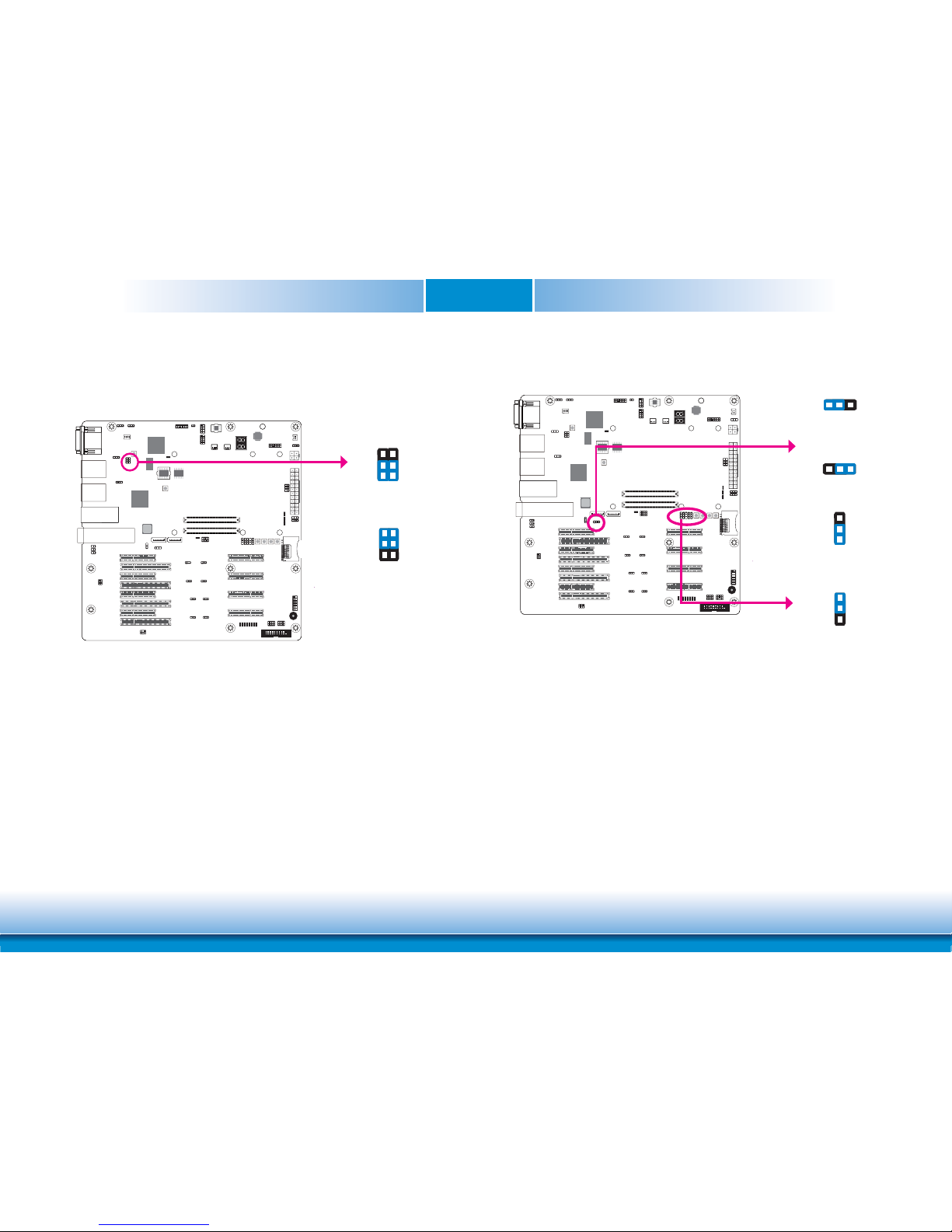
Jumper Settings
USB Power Select
JP1 (for USB 3.0 Ports 0,1) and JP2 (for USB 3.0 Ports 2,3) are used to select the power of
USB ports. Selecting +5VDU will allow you to use a USB keyboard to wake up the system.
USB 3.0 Ports 0,1
(JP1)
USB 3.0 Ports 2,3
(JP2)
2-3 On: +5VDU
1-2 On: +5V
(default)
312
312
Important:
If your module board supports Wake-On-USB Keyboard/Mouse function, the +5V_
standby power source of your power supply must support ≥2A for 2 USB devices.
Function Test Jumper
Battery Low Indicator
1
ON
2
3
4
J4
This jumper is used to simulate the signal status that indicates the external battery is low. By
setting J4 pins 1 and 2 to On, it sends a battery low signal to the module.
1-2 Off: Normal
(default)
1-2 On:
Battery low test
1 2
1 2
Page 9
www.dfi .comChapter 2 Hardware Installation
9
Chapter 2
1
ON
2
3
4
10G PHY Capability Select
JP9
The JP19 and JP9 are used to select the capability of 10G PHY lanes 0,1 and lanes 2,3 respectively.
If 10G_PHY_CAP_0,1 is tied low on the Carrier, this indicates to the Module that the PHY on
the Carrier for 10G interfaces 0 and 1 can be configured by either I
2
C or by MDIO.
If the Carrier leaves the line NC, then this indicates to the Module that the Carrier PHY can
only be configured by MDIO.
1
3
2
1
3
2
JP19
2-3 On:
MDIO or I
2
C
1-2 On:
MDIO only
(default)
312
312
1-2 On:
MDIO only
(default)
2-3 On:
MDIO or I
2
C
1
ON
2
3
4
USB 2.0 Port 3 Select
The JP4 is used to select the USB 2.0 port 3 connection path.
JP4
1-3, 2-4 On:
USB 2.0 Port 3
to Rear I/O Connector
5
1
3
2
4
6
3-5, 4-6 On:
USB 2.0 Port 3 to BMC
(default)
5
1
3
2
4
6
Page 10

www.dfi .comChapter 2 Hardware Installation
10
Chapter 2
1
ON
2
3
4
PCIe Lane Select
JP14
2-3 On
1-2 On (default)
312
312
The JP14 is used to select the PCIe Lanes 00~03: PCIe5 x4 slot (1-2 On) or PCIe1 x8 slot (2-3
On).
The JP10 is used to select the PCIe Lanes 04~07: PCIe9 x4 slot (1-2 On) or PCIe1 x8 slot (2-3
On).
The JP15 is used to select the PCIe Lanes 08~11: PCIe6 x4 slot (1-2 On) or PCIe2 x8 slot (2-3
On).
The JP11 is used to select the PCIe Lanes 12~15: PCIe10 x4 slot (1-2 On) or PCIe2 x8 slot
(2-3 On).
The JP12 is used to select the PCIe Lanes 16~19: PCIe7 x4 slot (1-2 On) or PCIe3 x8 slot (2-3
On).
The JP16 is used to select the PCIe Lanes 20~23: PCIe11 x4 slot (1-2 On) or PCIe3 x8 slot
(2-3 On).
The JP13 is used to select the PCIe Lanes 24~27: PCIe8 x4 slot (1-2 On) or PCIe4 x8 slot (2-3
On).
The JP17 is used to select the PCIe Lanes 28~31: PCIe12 x4 slot (1-2 On) or PCIe4 x8 slot
(2-3 On).
JP17
JP16
JP15
JP10
JP13
JP12
JP11
1
ON
2
3
4
PCIe Lane 12 Select
The JP18 is used to select PCIe Lane 12 to BMC or multiplexer.
3
1
2
JP18
1-2, 4-5, 7-8, 10-11 On:
PCIe Lane 12 to BMC
(default)
3
1
2
12
10
11
12
10
11
2-3, 5-6, 8-9, 11-12 On:
PCIe Lane 12 to Multiplexer
(Refer JP11 also)
Page 11

www.dfi .comChapter 2 Hardware Installation
11
Chapter 2
1
ON
2
3
4
TPM_PP on CB Select
The JP20 is used to select to turn on or off the TPM_PP on CB.
1
3
2
1
3
2
JP20
1-2 On:
On
2-3 On:
Off (default)
1
ON
2
3
4
ESPI- Enable Select
The JP21 is used to select to enable LPC BUS or ESPI- BUS.
1
3
2
1
3
2
JP21
1-2 On:
LPC BUS Enable
(default)
2-3 On:
ESPI- BUS Enable
Page 12

www.dfi .comChapter 2 Hardware Installation
12
Chapter 2
BIOS Boot Location Select
1
ON
2
3
4
JP23
The JP22 and JP23 are used to determine the BIOS boot location.
1
3
2
1
3
2
JP22
1
3
2
JP22 2-3 On, JP23 2-3 On:
SPI0 on Module (default)
1
3
2
1
3
2
JP22 2-3 On, JP23 1-2 On:
SPI0 on Carrier
1
3
2
JP22 1-2 On, JP23 1-2 On:
Module SPI Only
1
ON
2
3
4
PIN 0~3 DIO Output/Input Select
The JP24 and JP25 are used to select PIN 0~3 DIO output and input respectively.
3
1
2
JP24
1-2, 4-5, 7-8, 10-11 On:
LED off
3
1
2
12
10
11
12
10
11
JP25
2-3, 5-6, 8-9, 11-12 On:
LED on (default)
Page 13

www.dfi .comChapter 2 Hardware Installation
13
Chapter 2
VCC5_IN Power Select
1
ON
2
3
4
JP26
The JP26 is used to select the power rail for module VCC5_IN pins when in ATX or AT mode.
1-2 On:
+5V_standby (default)
3-4 On: +5V
5-6 On: NC
5
1
3
2
4
6
5
2
4
6
1
3
5
2
4
6
1
3
ATX/AT Mode Select (Power_OK)
1
ON
2
3
4
JP27
The JP27 allows you to select the PWR_OK connection state when setting power at ATX or AT
mode.
132
132
1-2 On:
PWR_OK from ATX PS PWR_OK
(default)
2-3 On:
PWR_OK from BMC GPO
13
2
1-X:
No PWR_OK when in AT Mode
Note:
JP27 and JP28 need to be set simultaneously. Please refer next page for JP28 description.
Page 14

www.dfi .comChapter 2 Hardware Installation
14
Chapter 2
Clear CMOS
If you encounter the following situations,
a) CMOS data becomes corrupted.
b) You forgot the supervisor or user password.
you can reconfigure the system with the default values stored in the ROM BIOS.
To load the default values stored in the ROM BIOS, please follow the steps below:
1. Power-off the system and unplug the power cord.
2. Set JP29 pins 2 and 3 to On. Wait for a few seconds and set JP29 back to its default setting, pins 1 and 2 On.
3. Now plug the power cord and power-on the system.
1-2 On:
Normal (default)
2-3 On:
Clear CMOS
1
ON
2
3
4
JP29
312
312
PS_ON Select
1
ON
2
3
4
JP28
The JP28 allows you to select the ATX mode auto power on or AT mode always on.
132
132
1-2 On:
ATX Mode Auto PWR_ON
(default)
2-3 On:
AT Mode Always ON
Note:
JP27 and JP28 need to be set simultaneously. Please refer last page for JP27 description.
Page 15

www.dfi .comChapter 2 Hardware Installation
15
Chapter 2
BMC UART1 Driver’s/Receiver’s Power Rail Select
1-2 On:
3V3 (Normal)
2-3 On:
3VDU (debug)
(default)
1
ON
2
3
4
JP31
312
312
BMC UART1 Port Mode Select
1
ON
2
3
4
JP30
The JP30 is used to select the mode of BMC UART1 port.
132
132
1-2 On:
Normal UART
2-3 On:
Debug mode (default)
The JP31 is used to select the driver’s/receiver’s power rail of the BMC UART1.
Note:
JP30 and JP31 need to be set simultaneously.
Note:
JP30 and JP31 need to be set simultaneously.
Page 16

www.dfi .comChapter 2 Hardware Installation
16
Chapter 2
BMC SPI1 Interface Mode Select
1
ON
2
3
4
SW1
To select BMC SPI1 interface mode, please use pins 1 and 2 of finger switch SW1.
BMC SPI1 Interface Mode Select SW1 Pins 1 & 2
Disable SPI Interface (default) 1 Off, 2 Off
Enable SPI Master 1 Off, 2 On
Reserved 1 On, 2 Off
Enable SPI Pass Through 1 On, 2 On
BMC 2nd Boot Watchdog Timer Select
1
ON
2
3
4
SW1
To enable or disable BMC 2nd boot watchdog timer, please use pin 3 of finger switch SW1.
BMC 2nd Boot Watchdog Timer Select SW1 Pin 3
Disable Off
Enable (default) On
Page 17

www.dfi .comChapter 2 Hardware Installation
17
Chapter 2
BMC MAC#1 Interface Type Select
1
ON
2
3
4
SW1
To select BMC MAC#1 interface type, please use pin 4 of finger switch SW1.
BMC MAC#1 Interface Type Select SW1 Pin 4
RMII/NCSI Off
RGMII (default) On
BMC VGA Select
1
ON
2
3
4
J20
1 2
1 2
1-X On: Normal
VGA/2D (default)
1-2 On:
Disable VGA
This jumper is used to disable BMC integrated VGA.
Page 18

www.dfi .comChapter 2 Hardware Installation
18
Chapter 2
Rear Panel I/O Ports
The rear panel I/O ports consist of the following:
• 1 BMC UART1/Debug port
• 1 VGA port
• 1 1G MGMT LAN port
• 1 1G RJ-45 LAN port
• 4 USB 3.0 ports
• 2 10G RJ-45 LAN ports
• 2 10G SFP+ LAN ports
BMC UART1/Debug
10G SFP+
LAN 1,2
USB 3.0
2,3
1G MGMT
LAN
1G RJ-45
LAN 1
VGA
USB 3.0
0,1
10G RJ-45
LAN 3,4
Graphics Interface
The display port consists of the following:
• 1 VGA port
1
ON
2
3
4
VGA
The VGA port is used for connecting a VGA monitor. Connect the monitor’s 15-pin D-shell cable
connector to the VGA port. After you plug the monitor’s cable connector into the VGA port,
gently tighten the cable screws to hold the connector in place.
Page 19

www.dfi .comChapter 2 Hardware Installation
19
Chapter 2
COM (Serial) Ports
The serial ports are asynchronous communication ports with 16C550A-compatible UARTs that
can be used with modems, serial printers, remote display terminals, and other serial devices.
1
ON
2
3
4
BMC UART1: RS232
BMC UART1/Debug
21
9
COM 1
COM 2
Pin COM1 COM2
1
NC NC
2
RX1 RX2
3
TX1 TX2
4
NC NC
5
GND GND
6
NC NC
7
NC NC
8
NC NC
9
NC NC
1
2345
6789
Pin BMC UART 1/Debug
1
DCD-
2
RD
3
TD
4
DTR-
5
GND
6
DSR-
7
RTS-
8
CTS-
9
RI-
Page 20

www.dfi .comChapter 2 Hardware Installation
20
Chapter 2
LAN Ports
The onboard LAN ports allow the system board to connect to a local area network by means
of a network hub.
1G MGMT LAN
1
ON
2
3
4
1G RJ-45 LAN 1
10G RJ-45 LAN 4
10G SFP+ LAN 1
10G RJ-45 LAN 3
10G SFP+ LAN 2
Wake-On-USB Keyboard/Mouse
The Wake-On-USB Keyboard/Mouse function allows you to use a USB keyboard or USB mouse
to wake up a system from the S3 (STR - Suspend To RAM) state. If your module board supports this function, follow below jumper setting to use it:
• Jumper Setting
JP1 (for USB 3.0 ports 0,1) and JP2 (for USB 3.0 ports 2,3) must be set to “2-3 On: +5VDU”.
Refer to “USB Power Select” in this chapter for more information.
Important:
If your module board supports Wake-On-USB Keyboard/Mouse function, the +5V_
standby power source of your power supply must support ≥2A for 2 USB devices.
USB Ports
USB allows data exchange between your computer and a wide range of simultaneously accessible external plug-and-play peripherals.
The system board is equipped with 4 onboard USB 3.0 ports (USB 0,1/2,3). (Full function
depends on module board.)
Driver Installation
You may need to install the proper drivers in your operating system to use the USB device.
Refer to your operating system’s manual or documentation for more information.
1
ON
2
3
4
USB 3.0
USB 2,3 USB 0,1
Page 21

www.dfi .comChapter 2 Hardware Installation
21
Chapter 2
I/O Connectors
LPC Connector
Digital I/O Connector
The 8-bit Digital I/O connector (4-bit GPI and 4-bit GPO) provides powering-on and control
functions to the connected external devices. The pin functions of the connector are listed as
the followings:
Pin Pin Assignment Pin Pin Assignment
1
GND
2
+12V
3
DIO7 (GPO3)
4
+12V
5
DIO6 (GPO2)
6
GND
7
DIO5 (GPO1)
8
+3.3V
9
DIO4 (GPO0)
10
+3.3V
11
DIO3 (GPI3)
12
GND
13
DIO2 (GPI2)
14
+5V_Standby
15
DIO1 (GPI1)
16
+5V_Standby
17
DIO0 (GPI0)
18
GND
19
GND
1
ON
2
3
4
2
1
19
DIO
1
ON
2
3
4
The Low Pin Count Interface was defined by Intel® Corporation to facilitate the industry’s
transition towards legacy free systems. It allows the integration of low-bandwidth legacy I/O
components within the system, which are typically provided by a Super I/O controller. Furthermore, it can be used to interface firmware hubs, Trusted Platform Module (TPM) devices and
embedded controller solutions. Data transfer on the LPC bus is implemented over a 4 bit serialized data interface, which uses a 24MHz LPC bus clock. For more information about LPC bus
refer to the Intel
®
Low Pin Count Interface Specification Revision 1.1’. The table on the right
indicates the pin functions of the LPC connector.
Pin Function Pin Function
1
L_CLK
2
L_AD1
3
L_RST#
4
L_AD0
5
L_FRAME# 6 3V3
7
L_AD3 8 GND
9
L_AD2 10 ---
11
L_SERIRQ 12 CLK_48MHz
13
5VSB 14 5V
LPC
2
1
14
13
Page 22

www.dfi .comChapter 2 Hardware Installation
22
Chapter 2
1
ON
2
3
4
7
RXN
GND
TXP
TXN
GND
1
RXP
GND
SATA 1SATA 0
SATA 3.0
SATA (Serial ATA) Connectors
The Serial ATA connectors are used to connect Serial ATA devices. Connect one end of the Serial ATA cable to a SATA connector and the other end to your Serial ATA device.
Cooling Fan Connectors
The fan connectors are used to connect cooling fans. The cooling fans will provide adequate
airflow throughout the chassis to prevent overheating the CPU and system board components.
1
ON
2
3
4
1
3
Sense
Power
Ground
System Fan 2
System Fan 1
Page 23

www.dfi .comChapter 2 Hardware Installation
23
Chapter 2
The 1-channel I2C bus interface conforms to the version 2.1 I2C bus specification. It operates
as a master or slave device and supports a multi-master bus.
I2C Header
1
ON
2
3
4
I2C
SMBus Header
The SMBus (System Management Bus) connector is used to connect the SMBus device. It is a
multiple device bus that allows multiple chips to connect to the same bus and enable each one
to act as a master by initiating data transfer.
1
ON
2
3
4
2
GND
3.3V DU
SMBUS_Data
SMBUS_CLK
SMBUS_Alert#
1
5
2
1
NC
I
2
C_DATA
I
2
C_Clock
GND
3V3 DU
5
SMBus
Page 24

www.dfi .comChapter 2 Hardware Installation
24
Chapter 2
Use a power supply that complies with the ATX12V Power Supply Design Guide Version 1.1.
An ATX12V power supply unit has a standard 24-pin ATX main power connector that must be
inserted into the 24-pin connector. The 4-pin +12V power connector enables the delivery of
more +12VDC current to the COM express module board and carrier board’s PCIe device.
The power connectors from the power supply unit are designed to fit the 24-pin and 4-pin
connectors in only one orientation. Make sure to find the proper orientation before plugging
the connectors.
Power Connectors
1
ON
2
3
4
13
24
Ground
Ground
+12V
+12V
Important:
The system board consumes a minimal amount of power. Due to its low power
consumption, you only need a 120W to 150W power supply. Every power supply has
its minimum load of power. If you use a greater than 150W power supply, the power
consumed by the system board may not attain its minimum load causing instability to
the entire system.
13
12 24
1
+3.3VDC
+3.3VDC
+5VDC
PWR_OK
+5VSB
+12VDC
+12VDC
+3.3VDC
+3.3VDC
-12VDC
PS_ON#
GND
GND
NC
+5VDC
+5VDC
+5VDC
GND
GND
GND
GND
GND
+5VDC
GND
1
ON
2
3
4
Battery
The lithium ion battery (CR2032 coin cell) powers the real-time clock and CMOS memory. It is
an auxiliary source of power when the main power is shut off.
Safety Measures
• Danger of explosion if battery incorrectly replaced.
• Replace only with the same or equivalent type recommended by the manufacturer.
• Dispose of used batteries according to local ordinance
.
Connect to the
battery connector
Battery
Battery
Connector
1
+3.3V
GND
2
Page 25

www.dfi .comChapter 2 Hardware Installation
25
Chapter 2
Pin Pin Assignment Pin Pin Assignment
N.C.
1 N.C.
PWR-LED
2 LED Power
HD-LED
3 HDD Power 4 LED Power
5 Signal 6 Signal
RESET
7 Ground
ATX-SW
8 Ground
9 RST Signal 10 Signal
N.C.
11 N.C.
Front Panel Connector
HD-LED - Hard Drive LED
This LED will light when the hard drive is being accessed.
RESET - Reset Switch
This switch allows you to reboot without having to power off the system.
PWR-LED - Power/Standby LED
When the system’s power is on, this LED will light. When the system is in the S1 (POS - Power
On Suspend) state, it will blink every second. When the system is in the S3 (STR - Suspend To
RAM) state, it will blink every 4 seconds.
ATX-SW - ATX Power Switch
This switch is used to power on or off the system.
1
ON
2
3
4
Front
Panel
12
11
2
1
HD-LED
RESET
PWR-LED
ATX- SW
Page 26

www.dfi .comChapter 2 Hardware Installation
26
Chapter 2
Expansion Slots
PCI Express x4 Slot
Install PCI Express cards such as network cards or other cards that comply to the PCI Express
specifications into the PCI Express x4 slot.
PCI Express x8 Slot
Install PCI Express cards such as network cards or other cards that comply to the PCI Express
specifications into the PCI Express x8 slot.
1
ON
2
3
4
PCIe 5 (PCIe x4)
PCIe 1 (PCIe x8)
PCIe 6 (PCIe x4)
PCIe 2 (PCIe x8)
PCIe 7 (PCIe x4)
PCIe 3 (PCIe x8)
PCIe 8 (PCIe x4)
PCIe 4 (PCIe x8)
PCIe 9 (PCIe x4)
PCIe 10 (PCIe x4)
PCIe 11 (PCIe x4)
PCIe 12 (PCIe x4)
COM Express Connectors
The COM Express connectors are used to interface the carrier board with a COM Express
board. Refer to the following pages for the pin functions of these connectors.
COM Express
Connectors (Type 7)
1
ON
2
3
4
Page 27

www.dfi .comChapter 2 Hardware Installation
27
Chapter 2
Pin Row C Row D
1 GND (FIXED) GND (FIXED)
2 GND GND
3 USB_SSRX0- USB_SSTX04 USB_SSRX0+ USB_SSTX0+
5 GND GND
6 USB_SSRX1- USB_SSTX17 USB_SSRX1+ USB_SSTX1+
8 GND GND
9 USB_SSRX2- USB_SSTX210 USB_SSRX2+ USB_SSTX2+
11 GND (FIXED) GND (FIXED)
12 USB_SSRX3- USB_SSTX313 USB_SSRX3+ USB_SSTX3+
14 GND GND
15 10G_PHY_MDC_SCL3 10G_PHY_MDIO_SDA3
16 10G_PHY_MDC_SCL2 10G_PHY_MDIO_SDA2
17 10G_SDP2 10G_SDP3
18 GND GND
19 PCIE_RX6+ PCIE_TX6+
20 PCIE_RX6- PCIE_TX621 GND (FIXED) GND (FIXED)
22 PCIE_RX7+ PCIE_TX7+
23 PCIE_RX7- PCIE_TX724 10G_INT2 10G_INT3
25 GND GND
26 10G_KR_RX3+ 10G_KR_TX3+
27 10G_KR_RX3- 10G_KR_TX328 GND GND
29 10G_KR_RX2+ 10G_KR_TX2+
30 10G_KR_RX2- 10G_KR_TX231 GND (FIXED) GND (FIXED)
32 10G_SFP_SDA3 10G_SFP_SCL3
33 10G_SFP_SDA2 10G_SFP_SCL2
34 10G_PHY_RST_23 10G_PHY_CAP_23
35 10G_PHY_RST_01 10G_PHY_CAP_01
36 10G_LED_SDA RSVD
37 10G_LED_SCL RSVD
38 10G_SFP_SDA1 10G_SFP_SCL1
39 10G_SFP_SDA0 10G_SFP_SCL0
40 10G_SDP0 10G_SDP1
41 GND (FIXED) GND (FIXED)
42 10G_KR_RX1+ 10G_KR_TX1+
43 10G_KR_RX1- 10G_KR_TX144 GND GND
45 10G_PHY_MDC_SCL1 10G_PHY_MDIO_SDA1USB0- USB1-
USB2- USB3USB2+ USB3+
USB_2_3_OC# USB_0_1_OC#
PCIE_TX12+ PCIE_RX12+
PCIE_TX12- PCIE_RX12GND (FIXED) GND (FIXED)
PCIE_TX13+ PCIE_RX13+
PCIE_TX13- PCIE_RX13GND GND
RSVD I2C_CK
BIOS_DIS0#/ESPI_SAFS I2C_DAT
THRMTRIP# THRM#
RSVD RSVD
GND (FIXED) GND (FIXED)
RSVD SPKR
BATLOW# WDT
(S)ATA_ACT# RSVD
RSVD RSVD
SUS_S5# PWR_OK
PCIE_TX14+ PCIE_RX14+
PCIE_TX14- PCIE_RX14-
GND (FIXED) GND (FIXED)
PCIE_TX15+ PCIE_RX15+
PCIE_TX15- PCIE_RX15-
SUS_S4# SUS_STAT#/ESPI_RESET#
SATA0_RX+ SATA1_RX+
SATA0_RX- SATA1_RX-
SUS_S3# SMB_ALERT#
SATA0_TX+ SATA1_TX+
SATA0_TX- SATA1_TX-
GBE0_MDI0- PWRBTN#
GBE0_MDI0+ SMB_CK
GBE0_CTREF SMB_DAT
GBE0_MDI1- LPC_DRQ1#/ESPI_ALERT1#
GBE0_MDI1+ LPC_CLK/ESPI_CK
GND (FIXED) GND (FIXED)
GBE0_MDI2- LPC_AD2/ESPI_IO_2
GBE0_MDI2+ LPC_AD3/ESPI_IO_3
GBE0_LINK# LPC_DRQ0#/ESPI_ALERT0#
GBE0_MDI3+ LPC_FRAME#/ESPI_CS0#
GBE0_LINK100# LPC_AD0/ESPI_IO_0
GBE0_LINK1000# LPC_AD1/ESPI_IO_1
Row A Row B
GND (FIXED) GND (FIXED)
GBE0_MDI3- GBE0_ACT#
Page 28

www.dfi .comChapter 2 Hardware Installation
28
Chapter 2
Pin Row B Row C Row D
46 USB1+ 10G_PHY_MDC_SCL0 10G_PHY_MDIO_SDA0
47 ESPI_EN# 10G_INT0 10G_INT1
48 USB0_HOST_PRSNT GND GND
49 SYS_RESET# 10G_KR_RX0+ 10G_KR_TX0+
50 CB_RESET# 10G_KR_RX0- 10G_KR_TX051 GND (FIXED) GND (FIXED) GND (FIXED)
52 PCIE_RX5+ PCIE_RX16+ PCIE_TX16+
53 PCIE_RX5- PCIE_RX16- PCIE_TX1654 GPO1/SD_CMD (opt.) TYPE0# RSVD
55 PCIE_RX4+ PCIE_RX17+ PCIE_TX17+
56 PCIE_RX4- PCIE_RX17- PCIE_TX1757 GPO2/SD_WP (opt.) TYPE1# TYPE2#
58 PCIE_RX3+ PCIE_RX18+ PCIE_TX18+
59 PCIE_RX3- PCIE_RX18- PCIE_TX1860 GND (FIXED) GND (FIXED) GND (FIXED)
61 PCIE_RX2+ PCIE_RX19+ PCIE_TX19+
62 PCIE_RX2- PCIE_RX19- PCIE_TX1963 GPO3/SD_CD# (opt.) RSVD RSVD
64 PCIE_RX1+ RSVD RSVD
65 PCIE_RX1- PCIE_RX20+ PCIE_TX20+
66 WAKE0# PCIE_RX20- PCIE_TX2067 WAKE1# RAPID_SHUTDOWN GND
68 PCIE_RX0+ PCIE_RX21+ PCIE_TX21+
69 PCIE_RX0- PCIE_RX21- PCIE_TX2170 GND (FIXED) GND (FIXED) GND (FIXED)
71 PCIE_RX8+ PCIE_RX22+ PCIE_TX22+
72 PCIE_RX8- PCIE_RX22- PCIE_TX2273 GND GND GND
74 PCIE_RX9+ PCIE_RX23+ PCIE_TX23+
75 PCIE_RX9- PCIE_RX23- PCIE_TX2376 GND GND GND
77 PCIE_RX10+ RSVD RSVD
78 PCIE_RX10- PCIE_RX24+ PCIE_TX24+
79 GND PCIE_RX24- PCIE_TX2480 GND (FIXED) GND (FIXED) GND (FIXED)
81 PCIE_RX11+ PCIE_RX25+ PCIE_TX25+
82 PCIE_RX11- PCIE_RX25- PCIE_TX2583 GND RSVD RSVD
84 VCC_5V_SBY GND GND
85 VCC_5V_SBY PCIE_RX26+ PCIE_TX26+
86 VCC_5V_SBY PCIE_RX26- PCIE_TX2687 VCC_5V_SBY GND GND
88 BIOS_DIS1# PCIE_RX27+ PCIE_TX27+
89 NCSI_RX_ER PCIE_RX27- PCIE_TX2790 GND (FIXED) GND (FIXED) GND (FIXED)
Row A
USB0+
VCC_RTC
RSVD
GBE0_SDP
LPC_SERIRQ/ESPI_CS1#
GND (FIXED)
PCIE_TX5+
PCIE_TX5GPI0/SD_DATA0 (opt.)
PCIE_TX4+
PCIE_TX4GND
PCIE_TX3+
PCIE_TX3GND (FIXED)
PCIE_TX2+
PCIE_TX2GPI1/SD_DATA1 (opt.)
PCIE_TX1+
PCIE_TX1GND
GPI2/SD_DATA2 (opt.)
PCIE_TX0+
PCIE_TX0GND (FIXED)
PCIE_TX8+
PCIE_TX8GND
PCIE_TX9+
PCIE_TX9GND
PCIE_TX10+
PCIE_TX10GND
GND (FIXED)
PCIE_TX11+
PCIE_TX11GND
NCSI_TX_EN
GPI3/SD_DATA3 (opt.)
RSVD
RSVD
PCIE_CK_REF+
PCIE_CK_REFGND (FIXED)
Page 29

www.dfi .comChapter 2 Hardware Installation
29
Chapter 2
91 NCSI_CLK_IN PCIE_RX28+ PCIE_TX28+
92 NCSI_RXD1 PCIE_RX28- PCIE_TX2893 NCSI_RXD0 GND GND
94 NCSI_CRS_DV PCIE_RX29+ PCIE_TX29+
95 NCSI_TXD1 PCIE_RX29- PCIE_TX2996 NCSI_TXD0 GND GND
97 SPI_CS# RSVD RSVD
98 NCSI_ARB_IN PCIE_RX30+ PCIE_TX30+
99 NCSI_ARB_OUT PCIE_RX30- PCIE_TX30100 GND (FIXED) GND (FIXED) GND (FIXED)
101 FAN_PWMOUT PCIE_RX31+ PCIE_TX31+
SPI_POWER
SPI_MISO
GPO0/SD_CLK (opt.)
SPI_CLK
GND (FIXED)
SER1_TX
SPI_MOSI
TPM_PP
TYPE10#
SER0_TX
SER0_RX
102 FAN_TACHIN PCIE_RX31- PCIE_TX31103 SLEEP# GND GND
104 VCC_12V VCC_12V VCC_12V
105 VCC_12V VCC_12V VCC_12V
106 VCC_12V VCC_12V VCC_12V
107 VCC_12V VCC_12V VCC_12V
108 VCC_12V VCC_12V VCC_12V
109 VCC_12V VCC_12V VCC_12V
110 GND (FIXED) GND (FIXED) GND (FIXED)
SER1_RX
LID#
VCC_12V
VCC_12V
VCC_12V
VCC_12V
VCC_12V
VCC_12V
GND (FIXED)
Pin Row B Row C Row DRow A
Page 30

www.dfi .comChapter 2 Hardware Installation
30
Chapter 2
Switches
• Lid: It is used to turn the LVDS on or off.
• Sleep: It is used to set the system to “sleep” or “wake-up” mode.
1
ON
2
3
4
Power
Reset
Lid
Sleep
Note:
The Sleep and Lid functions are supported only when your operating system supports
ACPI.
SDIO (optional)
This expansion port is used to insert a Secure Digital Input/Output (SDIO) or Multimedia Card
(MMC) device. Aside from storing data files, an SDIO card is also capable of storing powerful
software applications.
1
ON
2
3
4
SDIO
(optional)
BMC AST2500 Chip Level Reset
BMC AST2500 SOC Level Reset
Page 31

www.dfi .comChapter 2 Hardware Installation
31
Chapter 2
1
ON
2
3
4
BMC AST2500 Heart Beat LED
Thermal Trip LED
LEDs
Thermal Trip LED will light to indicate that the processor is on an overheating status.
BMC AST2500 Heart Beat LED indicates if the BMC SPI flash is programmed. The hardware
mode includes below blinking modes:
Indicator LED for Non-Type 7 Module Inserted
Indicator LED for Type 7 Module Inserted
Indicator LED for Type 6 Module Inserted
Debug LED
GPI3 LED
GPI2 LED
GPI1 LED
GPO0 LED
GPO1 LED
GPO2 LED
GPO3 LED
GPI0 LED
Inphi Configure Pin-Plug
1
ON
2
3
4
JP8
3
1
GND
CS4227 SCL (1.8V)
CS4227 SDA (1.8V)
0Hz
Always dark means fi rmware is not running or dead
0.1Hz
Abnormal mode, some interrupts are not serviced for over 2 seconds.
0.5Hz
Normal operation mode, ARM running on DRAM with interrupt monitor enabled
2Hz
ARM running on DRAM without interrupt enabled (instruction fetch from DRAM)
10Hz
ARM running on Flash (instruction fetch from fl ash)
Page 32

www.dfi .comChapter 2 Hardware Installation
32
Chapter 2
eSPI Female Header
1
ON
2
3
4
eSPI Female Header
The eSPI female header is reserved for future EXT-module.
2
1
14
13
 Loading...