

Page 1
COM100-B
COM Express Carrier Board
User’s Manual
A26100316
1
www.d.comChapter 1 Introduction
Page 2

Copyright
FCC and DOC Statement on Class B
This publication contains information that is protected by copyright. No part of it may be reproduced in any form or by any means or used to make any transformation/adaptation without
the prior written permission from the copyright holders.
This publication is provided for informational purposes only. The manufacturer makes no
representations or warranties with respect to the contents or use of this manual and specifically disclaims any express or implied warranties of merchantability or fitness for any particular
purpose. The user will assume the entire risk of the use or the results of the use of this document. Further, the manufacturer reserves the right to revise this publication and make changes
to its contents at any time, without obligation to notify any person or entity of such revisions
or changes.
Changes after the publication’s first release will be based on the product’s revision. The website
will always provide the most updated information.
© 2013. All Rights Reserved.
Trademarks
Product names or trademarks appearing in this manual are for identification purpose only and
are the properties of the respective owners.
This equipment has been tested and found to comply with the limits for a Class B digital
device, pursuant to Part 15 of the FCC rules. These limits are designed to provide reasonable protection against harmful interference when the equipment is operated in a residential
installation. This equipment generates, uses and can radiate radio frequency energy and, if not
installed and used in accordance with the instruction manual, may cause harmful interference
to radio communications. However, there is no guarantee that interference will not occur in a
particular installation. If this equipment does cause harmful interference to radio or television
reception, which can be determined by turning the equipment off and on, the user is encouraged to try to correct the interference by one or more of the following measures:
• Reorient or relocate the receiving antenna.
• Increase the separation between the equipment and the receiver.
• Connect the equipment into an outlet on a circuit different from that to which the receiver
is connected.
• Consult the dealer or an experienced radio TV technician for help.
Notice:
1. The changes or modifications not expressly approved by the party responsible for compliance could void the user’s authority to operate the equipment.
2. Shielded interface cables must be used in order to comply with the emission limits.
2
www.dfi .comChapter 1 Introduction
Page 3

Table of Contents
Copyright .............................................................................................................2
Trademarks ........................................................................................................2
FCC and DOC Statement on Class B .....................................................2
About this Manual ..........................................................................................4
Warranty ............................................................................................................4
Static Electricity Precautions ......................................................................4
Safety Measures ..............................................................................................4
About the Package .........................................................................................5
Chapter 1 - Introduction .............................................................................6
Specifications ................................................................................................6
Chapter 2 - Hardware Installation ................................................ 7
Board Layout .................................................................................................7
Block Diagram ...............................................................................................7
Mechanical Diagram ....................................................................................8
Jumper Settings ...........................................................................................9
USB Power Select ......................................................................................... 9
USB Mode Select ..........................................................................................9
Clear CMOS Data ........................................................................................ 10
Mini PCIe3 Signal Select ..............................................................................10
Mini PCIe3 Power Select ............................................................................. 11
Panel Power Select ..................................................................................... 11
VCC5_IN Power Select ................................................................................12
Super I/O Enable/Disable ............................................................................12
LCD/Inverter Power Select .......................................................................... 13
BIOS Select ................................................................................................13
DC-in Voltage Level .................................................................................... 14
Backlight Brightness Power Select ...............................................................14
Rear Panel I/O Ports .................................................................................15
5V~19V DC-in ............................................................................................ 15
Serial (COM) Ports ......................................................................................16
DisplayPort .................................................................................................16
RJ45 LAN Port ............................................................................................17
USB Ports ...................................................................................................17
Audio .........................................................................................................18
I/O Connectors ...........................................................................................18
S/PDIF Connector .......................................................................................18
Cooling Fan Connector ................................................................................ 19
Digital I/O Connector ..................................................................................19
LVDS LCD Panel Connector ......................................................................... 20
SATA (Serial ATA) Connector .......................................................................21
LPC Connector ............................................................................................ 21
Expansion Slots .......................................................................................... 22
Front Audio Connector ................................................................................ 23
Standby Power LED .................................................................................... 23
Front Panel Connector ................................................................................24
COM Express Connector .............................................................................. 25
Switches ....................................................................................................27
Serial Interface Connector ........................................................................... 27
2
I
C Connector ............................................................................................. 28
SMBus Connector .......................................................................................28
HDD Power Connector ................................................................................ 29
Battery .......................................................................................................29
Smart Battery Charger Connector ................................................................30
Chapter 3 - Supported Software .......................................................... 31
3
www.dfi .comChapter 1 Introduction
Page 4
About this Manual
Static Electricity Precautions
An electronic file of this manual is included in the CD. To view the user’s manual in the CD,
insert the CD into a CD-ROM drive. The autorun screen (Main Board Utility CD) will appear.
Click “User’s Manual” on the main menu.
Warranty
1. Warranty does not cover damages or failures that arised from misuse of the product,
inability to use the product, unauthorized replacement or alteration of components and
product specifications.
2. The warranty is void if the product has been subjected to physical abuse, improper installation, modification, accidents or unauthorized repair of the product.
3. Unless otherwise instructed in this user’s manual, the user may not, under any circumstances, attempt to perform service, adjustments or repairs on the product, whether in or
out of warranty. It must be returned to the purchase point, factory or authorized service
agency for all such work.
4. We will not be liable for any indirect, special, incidental or consequencial damages to the
product that has been modified or altered.
It is quite easy to inadvertently damage your PC, system board, components or devices even
before installing them in your system unit. Static electrical discharge can damage computer
components without causing any signs of physical damage. You must take extra care in handling them to ensure against electrostatic build-up.
1. To prevent electrostatic build-up, leave the system board in its anti-static bag until you are
ready to install it.
2. Wear an antistatic wrist strap.
3. Do all preparation work on a static-free surface.
4. Hold the device only by its edges. Be careful not to touch any of the components, contacts
or connections.
5. Avoid touching the pins or contacts on all modules and connectors. Hold modules or connectors by their ends.
Important:
Electrostatic discharge (ESD) can damage your processor, disk drive and other components. Perform the upgrade instruction procedures described at an ESD workstation only. If such a station is not available, you can provide some ESD protection by
wearing an antistatic wrist strap and attaching it to a metal part of the system chassis. If a wrist strap is unavailable, establish and maintain contact with the system
chassis throughout any procedures requiring ESD protection.
Safety Measures
To avoid damage to the system:
• Use the correct AC input voltage range.
To reduce the risk of electric shock:
• Unplug the power cord before removing the system chassis cover for installation or servicing. After installation or servicing, cover the system chassis before plugging the power
cord.
4
www.dfi .comChapter 1 Introduction
Page 5

About the Package
The package contains the following items. If any of these items are missing or damaged,
please contact your dealer or sales representative for assistance.
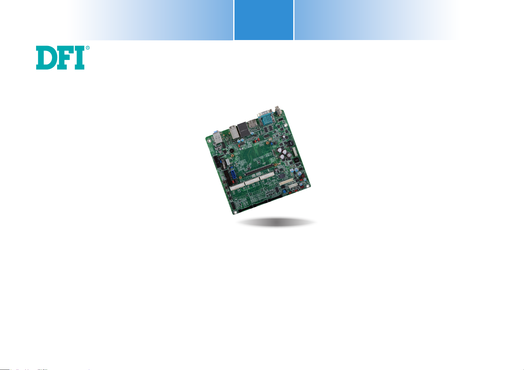
• One COM100-B board
• One SATA data cable
• One SATA power cable
• One IO shield
• One DVD
• One QR (Quick Reference)
Optional Items
• SATA data cable
• SATA power cable
• I/O shield
• Power adapter (60W, 12V)
The board and accessories in the package may not come similar to the information listed
above. This may differ in accordance with the sales region or models in which it was sold. For
more information about the standard package in your region, please contact your dealer or
sales representative.
Before Using the System Board
Before using the system board, prepare basic system components.
If you are installing the system board in a new system, you will need at least the following
internal components.
• A CPU
• Memory module
• Storage devices such as hard disk drive, CD-ROM, etc.
You will also need external system peripherals you intend to use which will normally include at
least a keyboard, a mouse and a video display monitor.
5
www.dfi .comChapter 1 Introduction
Page 6
Chapter 1 - Introduction
Specifications
Graphics
Audio
Storage
Digital I/O
Damage Free
Intelligence
Temperature
Humidity
Rear Panel IO
Ports
I/O Connectors
• Display pots
- 1 DisplayPort
- 1 24-bit single channel LVDS
• Realtek ALC886 7.1-channel High Defi nition Audio
• Audio outputs: Mic-in/Center+Subwoofer, line-in/surround and line out
• S/PDIF audio interface
• 1 SATA 3.0 ports with data transfer rate up to 6Gb/s
• 8-bit Digital I/O connector
- 4-bit GPI (General Purpose Input)
- 4-bit GPO (General Purpose Output)
• Legacy Super I/O support (optional)
- Monitors 5V/1.5V/12V/3.3V
- Monitors SIO_Fan
• Operating: 0oC to 60oC
• Storage: -20
• Operating: 10% to 90%
• 5V~19V DC-in jack
• 2 DB-9 RS232 serial ports
• 1 DisplayPort
• 1 RJ45 LAN port
• 2 USB 3.0 ports
• 4 USB 2.0 ports
• Line-in/Surround, Line out, and Mic-in/Center+Subwoofer jacks
• 1 serial interface for 2 serial ports (TX/RX)
• 1 LVDS LCD panel connector
• 1 LCD/inverter power connector
• 1 8-bit Digital I/O connector
• 1 front audio connector for line-out and mic-in jacks
• 1 S/PDIF connector
• 1 SATA 3.0 port
• 1 SATA power connector
• 1 Smart Battery charger connector
• 1 LPC connector
2
• 1 I
• 1 SMBus connector
• 1 front panel connector
• 2 fan connectors
o
C to 85oC
C connectors
Chapter 1
Expansion Slots
Supported COM
Express Module
ROM Interface
Power Output
PCB
• 1 PCIe x1 slot (PCIe 2.0)
• 3 Mini PCIe slots (PCIe 2.0)
- 1 slot supports PCIe and USB signals for 3G module
- 1 slot supports PCIe and USB signals
- 1 slot supports PCIe or mSATA signal
- Supports half/full size Mini PCIe card
• 1 SIM card socket
• Mini form factor
• 1 SPI interface
- Supports up to 64Mbit
• 12V, 5VSB, VCC_RTC (ATX Mode)
12V, 5V, VCC_RTC (AT mode)
12V, VCC_RTC (AT mode)
• Dimensions
- Mini-ITX form factor
- 170mm (6.7") x 170mm (6.7")
• Compliance
- PICMG COM Express
®
R2.1, Type 10
6
www.dfi .comChapter 1 Introduction
Page 7
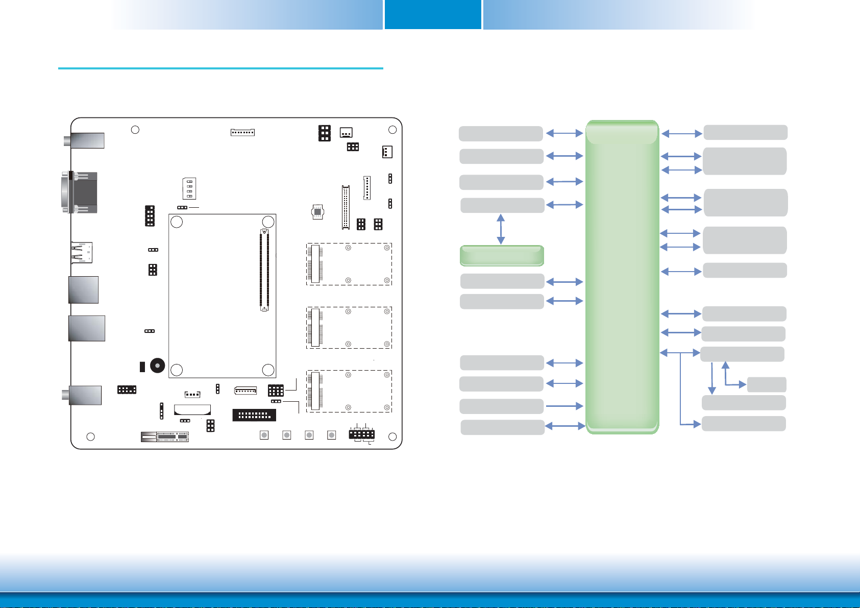
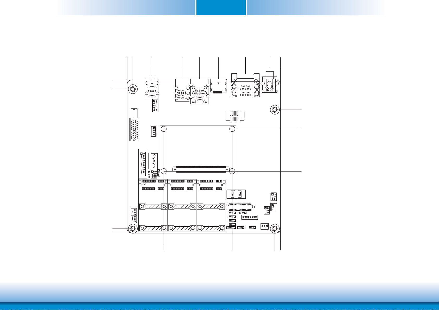
Chapter 2 - Hardware Installation
Board Layout
8
1
ON
4
1
Smart Battery Charge
Super I/O
Enable/Disable
(JP5)
1
USB Mode
Select (JP11)
56
SM
Bus
12
1
SATA 3.0
2
1
A110
B110
COM express connector
B1
A1
Mini PCIe3
Signal Select
(JP12)
3
12
1
10
1
DIO
Mini PCIe3
19
Power Select(JP13)
Sleep
Lid
DC-in jack
COM2
COM1
COM1
COM1
COM2
COM2
Display Port
LAN
USB 3.0
(0-1)
USB 2.0
(2-5)
Line-in
Line-out
Mic-in
910
12
USB 0-1 Power
Select (JP3)
1
1
2
5
6
VCC5_IN Power
Select (JP4)
USB 2-5 Power
Select (JP2)
1
Buzzer
Standby
Power LED
210
1
9
Front Audio
PCIe x1
S/PDIF
Clear CMOS (JP6)
Switch 5
1
234
1
LPC
HDD Power
1
Battery
1
1
2
I C
56
LVDS LCD
Panel
SPI
Flash
BIOS
Reset Power
2
SIO_Fan
1
6
2
Panel
Power
Select
5
1
(JP14)
8
4039
1
LCD/
Inverter
Power
1
4
3
Serial Interface 0/1
6
(Rx/Tx)
Mini PCIe 1
Mini PCIe 2
Mini PCIe3 mSATA
RESET HD-LED
11
ATX-SW
System_Fan
LCD/Inverter
Power Select
(JP18)
Backlight
Brightness
Power Select
(JP19)
1
4
BIOS
Select
(JP20)
3
6
RSVDRSVD
Front Panel
1
2
PWR-LED
1
1
1
Chapter 2
Block Diagram
GLAN
Audio Codec
SATA 3.0
SMBus
Smart Charger
I2C
Serial Port 2x
SYS Fan
Display Port
SLP & LID
USB 3.0 2x
TYPE 10
Connector
Row AB
PCIE
USB
PCIE
USB
PCIE
SATA
PCIE x1
Mini PCIE x1
Mini PCIE x1
Mini PCIE x1
(mSATA Opt.)
USB 2.0 4x
LVDS
GPIO
LPC Super IO
Fan
COM 2x
LPC
7
www.dfi .comChapter 2 Hardware Installation
Page 8
Mechanical Diagram
10.16
0.00
6.35
0.00
21.23
54.83
Chapter 2
73.83
94.89
124.83
151.76
163.65
22.86
44.14
154.94
159.84
34.21
8
110.21
157.48
91.14
163.65
www.dfi .comChapter 2 Hardware Installation
Page 9
Chapter 2
Jumper Settings
USB Power Select
COM2
COM1
COM1
COM2
USB 0-1
(JP3)
USB 2-5
(JP2)
312
1-2 On: +5V
(default)
312
2-3 On:
+5V_standby
USB Mode Select
COM2
COM1
COM1
COM2
JP11
JP3 (for USB 0-1) and JP2 (for USB 2-5) are used to select the power of USB ports. Selecting
+5V_standby will allow you to use a USB keyboard to wake up the system.
Important:
If you are using the Wake-On-USB Keyboard/Mouse function for 2 USB ports, the
+5V_standby power source of your power supply must support ≥1.5A. For 3 or more
USB ports, the +5V_standby power source of your power supply must support ≥2A.
The JP11 is used to select the USB mode.
9
3
2
1
1-2 On: NC
3
2
1
2-3 On: Host
(default)
www.dfi .comChapter 2 Hardware Installation
Page 10
Chapter 2
Clear CMOS Data
COM2
COM1
COM1
COM2
If you encounter the following situations,
JP6
312
1-2 On: Normal
(default)
312
2-3 On:
Clear CMOS Data
Mini PCIe3 Signal Select
COM2
COM1
COM1
COM2
3
1
1-4-7-10, 2-5-8-11 On:
JP12
3
1
2-5-8-11, 3-6-9-12 On:
mSATA (default)
The JP12 is used to select the Mini PCIe signal.
PCIe
12
10
12
10
a) CMOS data becomes corrupted.
b) You forgot the supervisor or user password.
you can reconfigure the system with the default values stored in the ROM BIOS.
To load the default values stored in the ROM BIOS, please follow the steps below:
1. Power-off the system and unplug the power cord.
2. Set JP6 pins 2 and 3 to On. Wait for a few seconds and set JP6 back to its default setting,
pins 1 and 2 On.
3. Now plug the power cord and power-on the system.
10
www.dfi .comChapter 2 Hardware Installation
Page 11

Chapter 2
Mini PCIe3 Power Select Panel Power Select
COM2
COM1
COM1
COM2
JP13
312
1-2 On: +3.3V
(default)
312
COM2
COM1
COM1
COM2
JP14
2
4
6
51
3
1-2 On: +12V
2
4
6
5
1
3
3-4 On:+5V
2
4
6
5
1
3
5-6 On: +3.3V
(default)
The JP13 is used to select the power supplied with the Mini PCIe.
2-3 On:
+3.3V_standby
The JP14 is used to select the power supplied with the LCD panel.
Important:
Before powering-on the system, make sure that the power settings of JP14 match
the LCD panel’s specification. Selecting the incorrect voltage will seriously damage the
LCD panel.
11
www.dfi .comChapter 2 Hardware Installation
Page 12

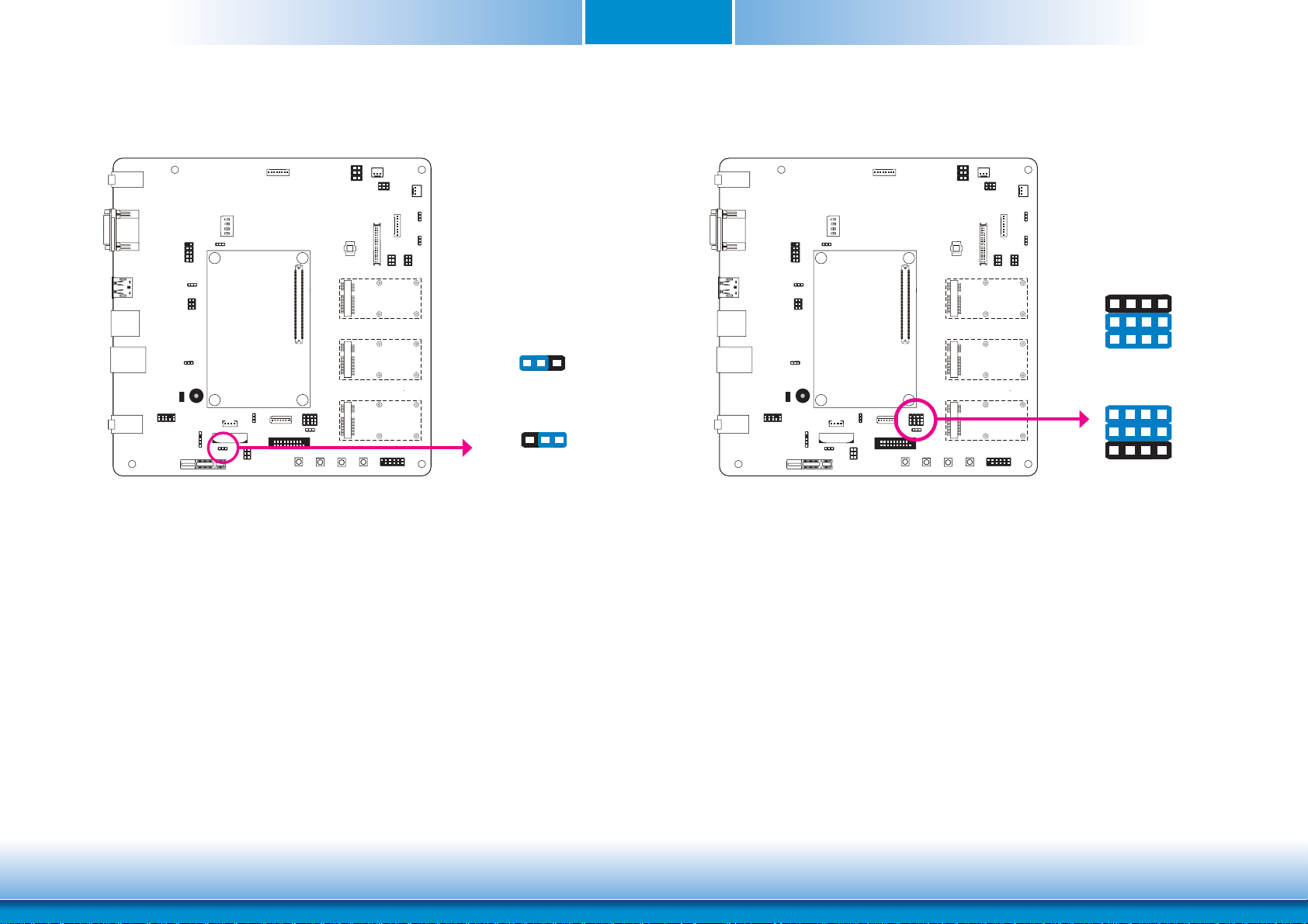
Chapter 2
VCC5_In Power Select
COM2
COM1
COM1
COM2
JP4
The JP4 is used to select the power of the COM Express connectors.
2
1
3
5
1-2 On: 5VSB
3
5
1
4
6
(default)
2
4
6
3-4 On: 5V
2
1
3
5
4
6
5-6 On: NC
Super I/O Enable/Disable
COM2
COM1
COM1
COM2
The JP5 is used to enable or disable the selection of Super I/O.
JP5
312
1-2 On: Enable
312
2-3 On: Disable
(default)
12
www.dfi .comChapter 2 Hardware Installation
Page 13

Chapter 2
LCD/Inverter Power Select
COM2
COM1
COM1
COM2
The JP18 is used to select the power level of LCD inverter connector.
JP18
1
2
3
1-2 On: +12V
1
2
3
2-3 On:
+5V (default)
BIOS Select
COM2
COM1
COM1
COM2
The JP20 is used to determine the BIOS boot device.
JP20
1
4
2
3
5
6
1-2 On, 4-5 On:
Module SPI BIOS
1
4
2
3
5
6
2-3 On, 4-5 On:
NC
1
2
3
4
5
6
1-2 On, 5-6 On:
Carrier SPI0
1
4
2
3
5
6
2-3 On, 5-6 On:
Module SPI0 (default)
13
www.dfi .comChapter 2 Hardware Installation
Page 14

Chapter 2
DC-in Voltage Level
on
1
1 On: 19V
2 On: 12V
2
(default)
3 On: 5V
3
4 On: NC
4
The Switch5 is used to select the voltage level of 5V~9V DC-in jack.
SW5
on on
on
COM2
COM1
COM1
COM2
Backlight Brightness Power Select
1
JP19
COM2
COM1
COM1
COM2
The JP19 is used to select the power level of backlight brightness control: +5V or +3.3V.
2
3
1-2 On: +5V
1
2
3
2-3 On: +3.3V
(default)
Important:
Before powering-on the system, make sure that the power settings of JP19 match the
power specification of backlight control. Selecting the incorrect voltage will seriously
damage the backlight.
14
www.dfi .comChapter 2 Hardware Installation
Page 15

Chapter 2
I C
Rear Panel I/O Ports
COM 1
DC-in jack
COM 2
The rear panel I/O ports consist of the following:
• 5V~19V DC-in jack
• 2 Serial COM ports
• 1 DisplayPort
• 1 LAN port
• 2 USB 3.0 ports
• 4 USB 2.0 ports
• Line-in/Surround, Line-out and Mic-in/Center+Subwoofer jacks
DisplayPort
LAN
USB 3.0
0-1
USB 2.0
2-5
Line-in/Surround
Line-out
Mic-in/
Center+Subwoofer
5V~19V DC-in
DC-in
This jack provides maximum of 60W power and is considered a low power solution. Connect
a DC power cord to this jack. Use a power adapter with 19V DC output voltage. Using a voltage higher than the recommended one may fail to boot the system or cause damage to the
system board.
COM2
COM1
COM1
COM2
15
www.d.comChapter 2 Hardware Installation
Page 16

Chapter 2
I C
I C
Serial (COM) Ports
COM 1
COM 2
COM 1 and COM 2:
RS232
The serial COM ports are RS232 asynchronous communication ports with 16C550A-compatible
UARTs that can be used with modems, serial printers, remote display terminals, and other serial devices.
COM2
COM1
COM1
COM2
DisplayPort
COM2
COM1
COM1
COM2
DisplayPort
DisplayPort is a digital display interface used to connect a display device such as a computer
monitor. It is used to transmit audio and video simultaneously. The interface, which is developed by VESA, delivers higher performance features than any other digital interface.
16
www.d.comChapter 2 Hardware Installation
Page 17

Chapter 2
I C
I C
RJ45 LAN Port
COM2
COM1
COM1
COM2
LAN
The onboard RJ45 LAN port allows the system board to connect to a local area network by
means of a network hub.
USB Ports
COM2
COM1
COM1
COM2
USB 0
USB 1
USB 3.0
USB 2
USB 3
USB 4
USB 5
USB 2.0
USB allows data exchange between your computer and a wide range of simultaneously accessible external Plug and Play peripherals.
The system board is equipped with two onboard USB 3.0/2.0/1.1 ports (USB 0-1) and four
onboard USB 2.0/1.2 ports (USB 2-5).
Driver Installation
You may need to install the proper drivers in your operating system to use the USB device.
Refer to your operating system’s manual or documentation for more information.
Wake-On-USB Keyboard/Mouse
The Wake-On-USB Keyboard/Mouse function allows you to use a USB keyboard or USB mouse
to wake up a system from the S3 (STR - Suspend To RAM) state. To use this function:
• Jumper Setting
JP3 (USB 0-1) and JP2 (USB 2-5) must be set to “2-3 On: +5V_standby”. Refer to “USB Power
Select” in this chapter for more information.
Important:
If you are using the Wake-On-USB Keyboard/Mouse function for 2 USB ports, the
+5V_standby power source of your power supply must support ≥1.5A. For 3 or more
USB ports, the +5V_standby power source of your power supply must support ≥2A.
17
www.d.comChapter 2 Hardware Installation
Page 18

Chapter 2
I C
I C
Audio
COM2
COM1
COM1
COM2
Line-in/Surround
Line-out
Center+Subwoofer
The system board is equipped with 3 audio jacks. A jack is a one-hole connecting interface for
inserting a plug.
• Line-in/Surround Jack (Light Blue)
This jack is used to connect any audio devices such as Hi-fi set, CD player, tape player, AM/FM
radio tuner, synthesizer, etc.
Mic-in/
2
1
AUD_GND
AUD_GND
AUD_HPRET_R
AUD_MIC
AUD_HPOUT_R
AUD_MIC_BIAS
Key
AUD_HPRET_L
10
9
5V Analog
AUD-HPOUT-L
Front Audio
I/O Connectors
S/PDIF Connector
COM2
COM1
COM1
COM2
+5V
SPDIF out
Ground
SPDIF in
The S/PDIF connectors are used to connect external S/PDIF ports. Your S/PDIF ports may be
mounted on a card-edge bracket. Install the card-edge bracket to an available slot at the rear
of the system chassis then connect the audio cable to the S/PDIF connector. Make sure pin 1
of the audio cable is aligned with pin 1 of the connector.
1
Key
S/PDIF
5
• Line-out Jack (Lime)
This jack is used to connect a headphone or external speakers.
• Mic-in/Center+Subwoofer (Pink)
This jack is used to connect to the center and subwoofer speakers of the audio system.
18
www.d.comChapter 2 Hardware Installation
Page 19

Chapter 2
I C
I C
Cooling Fan Connector
COM2
COM1
COM1
COM2
Power
Ground
Sense
1 3
SIO Fan
1
Ground
Sense
3
System Fan
Power
Digital I/O Connector
COM2
COM1
COM1
COM2
2
1
The 8-bit Digital I/O connector (4-bit GPI and 4-bit GPO) provides powering-on function to
external devices that are connected to these connectors. The pin functions of these connectors
are listed as the followings:
Pins Pin Assignment Pins Pin Assignment
DIO
19
The fan connectors are used to connect cooling fans. The cooling fans will provide adequate
airflow throughout the chassis to prevent overheating the CPU and system board components.
1
3
5
7
9
11
13
15
17
19
19
GND
DIO7
DIO6
DIO5
DIO4
DIO3
DIO2
DIO1
DIO0
GND
2
4
6
8
10
12
14
16
18
+12V
+12V
GND
+5V
+5V
GND
+5V_Standby
+5V_Standby
GND
www.d.comChapter 2 Hardware Installation
Page 20

Chapter 2
I C
LVDS LCD Panel Connector
LCD/Inverter Power Connector
LCD/Inverter power
8
COM2
COM1
COM1
COM2
The system board allows you to connect a LCD Display Panel by means of the LVDS
LCD panel connectors and the LCD/Inverter power connectors. These connectors transmit video signals and power from the system board to the LCD Display Panel.
Refer to the right side for the pin functions of these connectors.
Jumper Settings
Refer to the “Jumper Settings” section in this chapter for settings relevant to the LCD
panel.
1
LVDS LCD Panel
39
40
1
2
LVDS LCD Panel Connector
Pins Function Pins Function
1
3
5
7
9
11
13
15
17
19
21
23
25
27
29
31
33
35
37
39
GND
LVDS_Out3+
2
4
GND
LVDS_Out7+
LVDS_Out3- 6 LVDS_Out7-
GND 8 GND
LVDS_Out2+ 10 LVDS_Out6+
LVDS_Out2- 12 LVDS_Out6-
GND 14 GND
LVDS_Out1+ 16 LVDS_Out5+
LVDS_Out1- 18 LVDS_Out5-
GND 20 GND
LVDS_Out0+ 22 LVDS_Out4+
LVDS_Out0- 24 LVDS_Out4-
GND 26 GND
LVDS_CLK1+ 28 LVDS_CLK2+
LVDS_CLK1- 30 LVDS_CLK2-
GND 32 GND
LVDS_DDCCLK 34 N.C.
LVDS_DDCDAA 36 N.C.
Panel Power 38 Panel Power
Panel Power 40 Panel Power
LCD/Inverter Power Connector
Pins Function
1
2
Panel Inverter Brightness Voltage Control
3
4
5
6
Panel Backlight On/Off Control
7
8
GND
GND
Panel Power
+3.3V
+12V
+12V
Note:
DFI board's LVDS connector: Hirose DF13-40DP-1.25V(91)/40P/1.25mm; cable side
connector: Hirose DF13-40DS-1.25C.
20
www.d.comChapter 2 Hardware Installation
Page 21

Chapter 2
I C
I C
SATA (Serial ATA) Connector
COM2
COM1
COM1
COM2
TXN
TXP
RXN
GND
71
RXP
GND
GND
SATA 3.0
The Serial ATA connectors are used to connect Serial ATA devices. Connect one end of the Serial ATA cable to a SATA connector and the other end to your Serial ATA device.
LPC connector
COM2
COM1
COM1
LPC
10
LAD2
LAD3
FRAME#
RST#
CLK
GND
VCC3
LAD0
LAD1
291
The Low Pin Count Interface was defined by Intel® Corporation to facilitate the industry’s transition towards legacy free systems. It allows the integration of low-bandwidth legacy I/O components within the system, which are typically provided by a Super I/O controller. Furthermore,
it can be used to interface firmware hubs, Trusted Platform Module (TPM) devices and embedded controller solutions. Data transfer on the LPC bus is implemented over a 4 bit serialized
data interface, which uses a 33MHz LPC bus clock. For more information about LPC bus refer
to the Intel® Low Pin Count Interface Specification Revision 1.1’.
COM2
21
www.d.comChapter 2 Hardware Installation
Page 22

Chapter 2
I C
Expansion Slots
COM2
COM1
COM1
COM2
PCIe x1
Mini PCIe 1
(PCIe x1 and
USB Signal)
Mini PCIe 2
(PCIe x1, USB
and 3G Signal)
Mini PCIe 3
(PCIe x1/mSATA
Signal)
Mini PCIe Slot
The Mini PCIe socket is used to install a Mini PCIe card. Mini PCIe card is a small form factor
PCI card with the same signal protocol, electrical definitions, and configuration definitions as
the conventional PCI.
PCI Express x1 Slot
Install PCI Express cards such as network cards or other cards that comply to the PCI Express
specifications into the PCI Express x1 slot.
SIM Card Socket
The SIM slot on the system board is used to insert a SIM card.
SIM Card
Socket
22
www.d.comChapter 2 Hardware Installation
Page 23

Chapter 2
I C
I C
Front Audio Connector
GND
NC
Key
Line OUT-JD
Mic-JD
2
1
Mic IN-L
Mic IN-R
10
9
Front
GND
Line OUT-R
Audio
Line OUT-L
COM2
COM1
COM1
COM2
Standby Power LED
COM2
COM1
COM1
COM2
Standby Power LED
This LED will lit red when the system is in the standby mode. It indicates that there is power
on the system board. Power-off the PC then unplug the power cord prior to installing any devices. Failure to do so will cause severe damage to the motherboard and components.
The front audio connectors allow you to connect to the second line-out and mic-in jacks that
are at the front panel of your system.
23
www.d.comChapter 2 Hardware Installation
Page 24

Chapter 2
I C
Front Panel Connector
COM2
COM1
COM1
COM2
HDD-LED - HDD LED
This LED will light when the hard drive is being accessed.
RESET SW - Reset Switch
Front
Panel
RESET-SW
11
12
ATX-SW
HDD-LED
PWR-LED
Pin Pin Assignment Pin Pin Assignment
N.C.
HDD-LED
RESET SW
N.C.
1 N.C.
3
HDD Power
Signal
5 6 Signal
7
Ground
RST Signal
9 10 Ground
11 N.C. Key 12 Key
PWR-LED
2 LED Power
4 LED Power
PWR-BTN 8 Signal
1
2
This switch allows you to reboot without having to power off the system.
ATX-SW: ATX Power Switch
Depending on the setting in the BIOS setup, this switch is a “dual function power button” that
will allow your system to enter the Soft-Off or Suspend mode.
PWR-LED - Power/Standby LED
When the system’s power is on, this LED will light. When the system is in the S1 (POS - Power
On Suspend) state, it will blink every second. When the system is in the S3 (STR - Suspend To
RAM) state, it will blink every 4 seconds.
24
www.d.comChapter 2 Hardware Installation
Page 25

COM Express Connector
I C
Signal Descriptions
4.6.7 Type 6
Modules implementing Pin-out Type 6
shall
shall use the pin-out shown in this table. Refer to
Table 3.2 for minimum requirements and Table 3.4 for the order in which interfaces
shall
shall be
implemented.
Table 4.45: Pin List for Pin-out Type 6
COM2
COM1
COM1
COM2
The COM Express connectors are used to interface the carrier board with a COM Express
board. Refer to the following pages for the pin functions of these connectors.
COM Express
Connectors (Type 10)
Chapter 2
Pin Row A Row B Row C Row D
1 GND(FIXED) GND(FIXED) GND( FIXED) GND(FIXED)
2 GBE0_MDI3- GBE0_ACT# GND GND
3 GBE0_MDI3+ LPC_FRAME# USB_SSRX0- USB_SSTX0-
4 GBE0_LINK100# LPC_AD0 USB_SSRX0+ USB_SSTX0+
5 GBE0_LINK1000# LPC_AD 1 GND GND
6 GBE0_MDI2- LPC_AD2 USB_SSRX1- USB_SST X1-
7 GBE0_MDI2+ LPC_AD3 USB_SSRX1+ USB_SSTX1+
8 GBE0_LINK# LPC_DRQ0# GND GND
9 GBE0_MDI1- LPC_DRQ1# USB_SSRX2- USB_SSTX2-
10 GBE0_MDI1+ LPC_CLK USB_SSRX2+ USB_SSTX2+
11 GND(FIXED) GND(FIXED) GND(FIXED) GND(FIXED)
12 GBE0_MDI0- PWRBTN# USB_SSRX3- USB_SSTX3-
13 GBE0_MDI0+ SMB_CK USB_SSRX3+ USB_SSTX3+
14 GBE0_CTREF SMB_DAT GND GND
15 SUS_S3# SMB_ALERT# DDI1_PAIR6+ DDI1_CTRLCLK_AUX+
16 SATA0_TX+ SATA1_TX+ DDI1_PAIR6- DDI1_CTRLDATA_AUX-
17 SATA0_TX- SATA1_TX- RSVD
18 SUS_S4# SUS_STAT# RSVD
19 SATA0_RX+ SATA1_RX + PCIE_RX6+ PCIE_TX6+
20 SATA0_RX- SATA1_RX- PCIE_RX6- PCIE_TX6-
21 GND(FIXED) GND(FIXED) GND(FIXED) GND(FIXED)
22 SATA2_TX+ SATA3_TX+ PCIE_RX7+ PCIE_TX7+
23 SATA2_TX- SATA3_TX- PCIE_RX7- PCIE_TX7-
24 SUS_S5# PWR_OK DDI1_HPD RSVD
25 SATA2_RX+ SATA3_RX + DDI1_PAIR4 + RSVD
26 SATA2_RX- SATA3_RX- DDI1_PAIR4- DDI1_PAIR0+
27 BATLOW# W DT RSVD
28 (S)ATA_ACT# AC/HDA_SDIN2 RSVD
29 AC/HDA_SYNC AC/HDA_SDIN1 DDI1_PAIR5+ DDI1_PAIR1+
30 AC/HDA_RST# AC/HDA_SDIN0 DDI1_PAIR5- DDI1_PAIR1-
31 GND(FIXED) GND(FIXED) GND(FIXED) GND(FIXED)
32 AC/HDA_BITCLK SPKR DDI2_CTRLCLK_AUX+ DDI1_PAIR2+
33 AC/HDA_SDOUT I2C_CK DDI2_CTRLDATA_AUX- DDI1_PAIR2-
34 BIOS_DIS0# I2C_DAT DDI2_DDC_AUX_SEL DDI1_DDC_AUX_SEL
35 THRMTRIP# T HRM# RSVD
36 USB6- USB7- DDI3_CTRLCLK_AUX+ DDI1_PAIR3+
37 USB6+ USB7+ DDI3_CTRLDATA_AUX- DDI1_PAIR3-
38 USB_6_7_OC# USB_4_5_OC# DDI3_DDC_AUX_SEL RSVD
39 USB4- USB5- DDI3_PAIR0+ DDI2_PAIR 0+
40 USB4+ USB5+ DDI3_PAIR0- DDI2_PAIR0-
41 GND(FIXED) GND(FIXED) GND(FIXED) GND(FIXED)
19
19
19
19
19
19
RSVD
19
RSVD
19
19
DDI1_PAIR0-
19
RSVD
19
RSVD
19
25
www.d.comChapter 2 Hardware Installation
Page 26

Chapter 2
Signal Descriptions
Signal Descriptions
Pin Row A Row B Row C Row D
42 USB2- USB3- DDI3_PAIR1+ DDI2_PAIR1+
43 USB2+ USB3+ DDI3_PAIR1- DDI2_PAIR1-
44 USB_2_3_OC# USB_0_1_OC# DDI3_HPD DDI2_HPD
45 USB0- USB1- RSVD
46 USB0+ USB1+ DDI3_PAIR2+ DDI2_PAIR2+
47 VCC_RTC EXCD1_PERST# DDI3_PAIR2- DDI2_PAIR2-
48 EXCD0_PERST# EXCD1_CPP E# RSVD
49 EXCD0_CPPE# SYS_RESET# DDI3_PAIR3+ DDI2_PAIR 3+
50 LPC_SERIRQ CB_RESET# DDI3_PAIR3- DDI2_PAIR3-
51 GND(FIXED) GND(FIXED) GND(FIXED) GND(FIXED)
52 PCIE_TX5+ PCIE_R X5+ PEG_RX0+ PEG_TX0+
53 PCIE_TX5- PCIE_RX5- PEG_RX0- PEG_TX0-
54 GPI0 GPO1 TYPE0# PEG_LANE_RV#
55 PCIE_TX4+ PCIE_R X4+ PEG_RX1+ PEG_TX1+
56 PCIE_TX4- PCIE_RX4- PEG_RX1- PEG_TX1-
57 GND GPO2 TYPE1# T YPE2#
58 PCIE_TX3+ PCIE_R X3+ PEG_RX2+ PEG_TX2+
59 PCIE_TX3- PCIE_RX3- PEG_RX2- PEG_TX2-
60 GND(FIXED) GND(FIXED) GND(FIXED) GND(FIXED)
61 PCIE_TX2+ PCIE_R X2+ PEG_RX3+ PEG_TX3+
62 PCIE_TX2- PCIE_RX2- PEG_RX3- PEG_TX3-
63 GPI1 GPO3 RSVD
64 PCIE_TX1+ PCIE_R X1+ RSVD
65 PCIE_TX1- PCIE_RX1- PEG_RX4+ PEG_TX4+
66 GND WAKE0# PEG_RX4- PEG_TX4-
67 GPI2 WAKE1# RSVD
68 PCIE_TX0+ PCIE_R X0+ PEG_RX5+ PEG_TX5+
69 PCIE_TX0- PCIE_RX0- PEG_RX5- PEG_TX5-
70 GND(FIXED) GND(FIXED) GND(FIXED) GND(FIXED)
71 LVDS_A0+ LVDS_B0+ PEG_RX6+ PEG_TX6+
72 LVDS_A0- LVDS_B0- PEG_RX6- PEG_TX6-
73 LVDS_A1+ LVDS_B1+ GND GND
74 LVDS_A1- LVDS_B1- PEG_RX7+ PEG_TX7+
75 LVDS_A2+ LVDS_B2+ PEG_RX7- PEG_TX7-
76 LVDS_A2- LVDS_B2- GND GND
77 LVDS_VDD_EN LVDS_B3+ RSVD
78 LVDS_A3+ LVDS_B3- PEG_RX8+ PEG_TX8+
79 LVDS_A3- LVDS_BKLT_EN PEG_RX8- PEG_TX8-
80 GND(FIXED) GND(FIXED) GND(FIXED) GND(FIXED)
81 LVDS_A_CK+ LVDS_ B_CK+ PEG_RX 9+ PEG_TX9+
82 LVDS_A_CK- LVDS_B_CK- PEG_RX9- PEG_TX9-
83 LVDS_I2C_CK LVDS_BKLT_CT RL RSVD
84 LVDS_I2C_DAT VCC_5V_SBY GND GND
85 GPI3 VCC_5V_SBY PEG _RX10+ PEG_TX 10+
19
86 RSVD
VCC_5V_SBY PEG _RX10- PEG_TX 10-
87 eDP_HPD VCC_5V_SBY GND GND
88 PCIE_CLK_REF+ BIOS_DIS1 # PEG_RX11+ PEG_TX11+
89 PCIE_CLK_REF- VGA_RED PEG_RX11- PEG_TX11-
90 GND(FIXED) GND(FIXED) GND(FIXED) GND(FIXED)
19
19
19
19
19
19
19
RSVD
RSVD
RSVD
RSVD
GND
RSVD
RSVD
19
19
19
19
19
19
Pin Row A Row B Row C Row D
91 SPI_POWER VGA_GRN PEG_RX12+ PEG_TX12+
92 SPI_MISO VGA_BLU PEG_RX12- PEG_TX12-
93 GPO0 VGA_HSYNC GND GND
94 SPI_CLK VGA_VSYNC P EG_RX13+ PEG_TX13+
95 SPI_MOSI VGA_I 2C_CK PEG_RX13- PEG_TX13-
96 TPM_PP VGA_I2C_DAT GND GND
97 TYPE10# SPI_CS# RSVD
98 SER0_TX RSVD
99 SER0_RX RSVD
19
19
100 GND(FIXED) GND(FIXED) GND(FIXED) GND(FIXED)
101 SER1_TX FAN_PWNOUT PEG_RX15+ PEG_T X15+
102 SER1_RX FAN_TACHIN PEG_RX15- PEG_TX15-
103 LID# SLEEP# GND GND
104 VCC_12V VCC_12V VCC_12V VCC_12V
105 VCC_12V VCC_12V VCC_12V VCC_12V
106 VCC_12V VCC_12V VCC_12V VCC_12V
107 VCC_12V VCC_12V VCC_12V VCC_12V
108 VCC_12V VCC_12V VCC_12V VCC_12V
109 VCC_12V VCC_12V VCC_12V VCC_12V
110 GND(FIXED) GND(FIXED) GND(FIXED) GND(FIXED)
19
RSVD
19
PEG_RX14+ PEG_TX14+
PEG_RX14- PEG_TX14-
26
www.d.comChapter 2 Hardware Installation
Page 27

Chapter 2
Switches
COM2
COM1
COM1
COM2
Sleep
Lid
Reset
Power
Serial Interface Connector
COM2
COM1
COM1
COM2
GND
Serial Interface 0/1 (Rx/Tx)
The serial interface connector is used for 2 serial ports supported by Tx and Rx signals.
TX0
RX0
14
3
6
TX1
RX1
GND
Note:
The Sleep and Lid functions are supported only when your operating system supports
ACPI.
• Lid: it is used to turn the LVDS on or off.
• Sleep: it is used to set the system to “sleep” or “wake-up” mode.
27
www.dfi .comChapter 2 Hardware Installation
Page 28

Chapter 2
I C
I C
I2C Connector
COM2
COM1
COM1
COM2
3V3 Standby
I2C_Clock
NC
The 1-channel I2C bus interface conforms to the version 2.1 I2C bus specification. It operates
as a master or slave device and supports a multi-master bus.
1 2
5
I2C
6
GND
I2C_DATA
NC
SMBus Connector
COM2
COM1
COM1
COM2
SMBus
6 5
NC
SMB_DATA
GND
The SMBus (System Management Bus) connectors are used to connect the SMBus device. It is
a multiple device bus that allows multiple chips to connect to the same bus and enable each
one to act as a master by initiating data transfer.
SMB_ALERT
SMB_CLK
3V3SB
2
1
28
www.d.comChapter 2 Hardware Installation
Page 29

Chapter 2
I C
I C
HDD Power Connector
COM2
COM1
COM1
COM2
Ground
Ground
+12V +5V
1
The HDD power connectors supply power to the SATA drive. Connect one end of the provided
power cable to the HDD power connector and the other end to your storage device.
HDD Power
Battery
COM2
COM1
COM1
COM2
Battery
The lithium ion battery powers the real-time clock and CMOS memory. It is an auxiliary source
of power when the main power is shut off.
Safety Measures
• Danger of explosion if battery incorrectly replaced.
• Replace only with the same or equivalent type recommend by the manufacturer.
• Dispose of used batteries according to local ordinance.
29
www.d.comChapter 2 Hardware Installation
Page 30

Smart Battery Charger Connector
COM2
COM1
COM1
COM2
Smart Battery
Charger connector
18
Chapter 2
The smart batery charger connectors are used for the function of power mamgement and
determines the accurate battery capacity in the system operation. The functions of each pin
are listed as the followings:
Pins Function
1
2
3
4
5
6
7
8
V+
V+
NC
SMBus_CLK
SMBus_DATA
NC
V- (GND)
V- (GND)
30
www.dfi .comChapter 2 Hardware Installation
Page 31

Chapter 3 - Supported Software
The CD that came with the system board contains drivers, utilities and software applications
required to enhance the performance of the system board.
Insert the CD into a CD-ROM drive. The autorun screen (Mainboard Utility CD) will appear. If
after inserting the CD, “Autorun” did not automatically start (which is, the Mainboard Utility
CD screen did not appear), please go directly to the root directory of the CD and double-click
“Setup”.
Chapter 3
Audio Drivers
To install the driver, click “Audio Drivers” on the main menu.
1. Setup is now ready to install the
audio driver. Click Next.
2. Follow the remainder of the steps
on the screen; clicking “Next”
each time you finish a step.
3. Click “Yes, I want to restart my
computer now” then click Finish.
Restarting the system will allow
the new software installation to
take effect.
31
www.d.comChapter 3 Supported Software
Page 32

Adobe Acrobat Reader 9.3
To install the reader, click “Adobe Acrobat Reader 9.3” on the main menu.
1. Click Next to install or click
Change Destination Folder to
select another folder.
2. Click Install to begin installation.
Chapter 3
3. Click Finish to exit installation.
32
www.d.comChapter 3 Supported Software
 Loading...