

Page 1
www.dfi .comChapter 1 Introduction
1
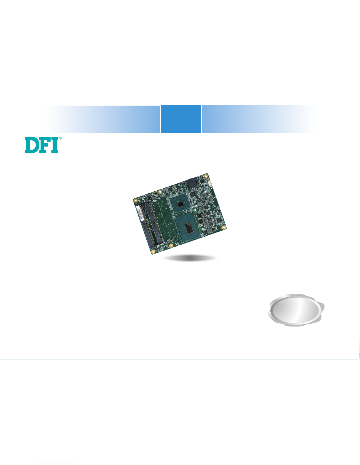
CH960-CM246/QM370/HM370
COM Express Basic Module
User’s Manual
A48600910
Preliminary
Version
Page 2

www.dfi .comChapter 1 Introduction
2
Copyright
This publication contains information that is protected by copyright. No part of it may be reproduced in any form or by any means or used to make any transformation/adaptation without
the prior written permission from the copyright holders.
This publication is provided for informational purposes only. The manufacturer makes no
representations or warranties with respect to the contents or use of this manual and specifically disclaims any express or implied warranties of merchantability or fitness for any particular
purpose. The user will assume the entire risk of the use or the results of the use of this document. Further, the manufacturer reserves the right to revise this publication and make changes
to its contents at any time, without obligation to notify any person or entity of such revisions
or changes.
Changes after the publication’s first release will be based on the product’s revision. The website
will always provide the most updated information.
© 2019. All Rights Reserved.
Trademarks
Product names or trademarks appearing in this manual are for identification purpose only and
are the properties of the respective owners.
COM Express Specification Reference
PICMG® COM Express ModuleTM Base Specification.
https://www.picmg.org/
FCC and DOC Statement on Class B
This equipment has been tested and found to comply with the limits for a Class B digital
device, pursuant to Part 15 of the FCC rules. These limits are designed to provide reasonable protection against harmful interference when the equipment is operated in a residential
installation. This equipment generates, uses and can radiate radio frequency energy and, if not
installed and used in accordance with the instruction manual, may cause harmful interference
to radio communications. However, there is no guarantee that interference will not occur in a
particular installation. If this equipment does cause harmful interference to radio or television
reception, which can be determined by turning the equipment off and on, the user is encouraged to try to correct the interference by one or more of the following measures:
• Reorient or relocate the receiving antenna.
• Increase the separation between the equipment and the receiver.
• Connect the equipment into an outlet on a circuit different from that to which the receiver
is connected.
• Consult the dealer or an experienced radio TV technician for help.
Notice:
1. The changes or modifications not expressly approved by the party responsible for compliance could void the user’s authority to operate the equipment.
2. Shielded interface cables must be used in order to comply with the emission limits.
Page 3

www.dfi .comChapter 1 Introduction
3
Table of Contents
Copyright ........................................................................................................... ..2
Trademarks ........................................................................................................2
COM Express Specification Reference ................................................... 2
FCC and DOC Statement on Class B ..................................................... 2
Warranty .............................................................................................................. 4
Static Electricity Precautions ...................................................................... 4
Safety Measures ..............................................................................................4
About the Package .........................................................................................5
Optional Items..................................................................................................5
Before Using the System Board ............................................................... 5
Chapter 1 - Introduction .............................................................................6
Specifications ................................................................................................6
Features ..........................................................................................................7
Chapter 2 - Concept ....................................................................... 8
COM Express Module Standards .............................................................. 8
Specification Comparison Table ...............................................................9
Chapter 3 - Hardware Installation .............................................. 10
Board Layout ............................................................................................... 10
Block Diagram ............................................................................................. 11
System Memory .......................................................................................... 12
Installing the SODIMM Module ...................................................................12
Connectors ................................................................................................... 13
CPU Fan Connector ..................................................................................... 13
COM Express Connectors ............................................................................14
COM Express Connectors Signals and Descriptions ....................................... 16
Standby Power LED ................................................................................... 27
Cooling Option ............................................................................................ 27
Heat Sink with Fan .....................................................................................27
Installing CH960-CM246/QM370/HM370 onto a Carrier Board .... 28
Chapter 4 - BIOS Setup ............................................................... 30
Overview....................................................................................................... 30
AMI BIOS Setup Utility ............................................................................. 31
Main .......................................................................................................... 31
Advanced ................................................................................................... 32
Chipset ...................................................................................................... 44
Security ...................................................................................................... 47
Boot........................................................................................................... 48
Save & Exit ................................................................................................49
Updating the BIOS .................................................................................... 49
Notice: BIOS SPI ROM ............................................................................. 50
Chapter 5 - Supported Software ........................................................... 51
Chapter 6 - RAID (CH960-CM246/QM370 only)........................58
Chapter 7 - Intel AMT Settings (CH960-CM246/QM370 only)
............................................................................................................................... 60
Page 4

www.dfi .comChapter 1 Introduction
4
Warranty
1. Warranty does not cover damages or failures that arised from misuse of the product, inability to use the product, unauthorized replacement or alteration of components and product specifications.
2. The warranty is void if the product has been subjected to physical abuse, improper installation, modification, accidents or unauthorized repair of the product.
3. Unless otherwise instructed in this user’s manual, the user may not, under any circumstances, attempt to perform service, adjustments or repairs on the product, whether in or
out of warranty. It must be returned to the purchase point, factory or authorized service
agency for all such work.
4. We will not be liable for any indirect, special, incidental or consequential damages to the
product that has been modified or altered.
Static Electricity Precautions
It is quite easy to inadvertently damage your PC, system board, components or devices even
before installing them in your system unit. Static electrical discharge can damage computer
components without causing any signs of physical damage. You must take extra care in handling them to ensure against electrostatic build-up.
1. To prevent electrostatic build-up, leave the system board in its anti-static bag until you are
ready to install it.
2. Wear an antistatic wrist strap.
3. Do all preparation work on a static-free surface.
4. Hold the device only by its edges. Be careful not to touch any of the components, contacts
or connections.
5. Avoid touching the pins or contacts on all modules and connectors. Hold modules or connectors by their ends.
Safety Measures
To avoid damage to the system:
• Use the correct AC input voltage range.
To reduce the risk of electric shock:
• Unplug the power cord before removing the system chassis cover for installation or servicing. After installation or servicing, cover the system chassis before plugging the power
cord.
Important:
Electrostatic discharge (ESD) can damage your processor, disk drive and other components. Perform the upgrade instruction procedures described at an ESD workstation only. If such a station is not available, you can provide some ESD protection by
wearing an antistatic wrist strap and attaching it to a metal part of the system chassis. If a wrist strap is unavailable, establish and maintain contact with the system
chassis throughout any procedures requiring ESD protection.
Page 5

www.dfi .comChapter 1 Introduction
5
About the Package
The package contains the following items. If any of these items are missing or damaged,
please contact your dealer or sales representative for assistance.
• One CH960-CM246/QM370/HM370 board
• One Cooler (Height: 36.58mm)
Optional Items
• COM332-B carrier board kit
• Heat spreader (Height: 11mm)
The board and accessories in the package may not come similar to the information listed
above. This may differ in accordance with the sales region or models in which it was sold. For
more information about the standard package in your region, please contact your dealer or
sales representative.
Before Using the System Board
Before using the system board, prepare basic system components.
If you are installing the system board in a new system, you will need at least the following
internal components.
• Memory module
• Storage devices such as hard disk drive, etc.
You will also need external system peripherals you intend to use which will normally include at
least a keyboard, a mouse and a video display monitor.
Page 6

www.dfi .comChapter 1 Introduction
6
Chapter 1 - Introduction
Specifications
Chapter 1
AUDIO Interface HD Audio
ETHERNET Controller CH960-CM246/QM370:
1 x Intel® I219LM with iAMT12.0 PCIe (10/100/1000Mbps)
CH960-HM370:
1 x Intel® I219LM PCIe (10/100/1000Mbps)
I/O USB 4 x USB 3.1
8 x USB 2.0
SATA CH960-CM246/QM370:
4 x SATA 3.0 (up to 6Gb/s)
RAID 0/1/5/10
CH960-HM370:
4 x SATA 3.0 (up to 6Gb/s)
DIO 1 x 8-bit DIO (Default 4 inputs and 4 outputs)
WATCHDOG
TIMER
Output &
Interval
System Reset, Programmable via Software from 1 to 255 Seconds
SECURITY TPM Available upon request
POWER Type 12V, 5VSB, VCC_RTC (ATX mode)
12V, VCC_RTC (AT mode)
OS SUPPORT Windows: Windows 10 IoT Enterprise 64-bit
Linux: Ubuntu 18.04
ENVIRONMENT Temperature Operating: 0 to 60°C or -40 to 85°C (with heat spreader)
Storage: -40 to 85°C
Humidity Operating: 5 to 90% RH
Storage: 5 to 90% RH
MECHANICAL Dimensions COM Express® Basic
95mm (3.74") x 125mm (4.9")
Compliance PICMG COM Express
®
R2.1, Type 6
SYSTEM Processor CH960-CM246/QM370:
8th Generation Intel
®
Core™ Processors, BGA 1440
Intel
®
Xeon® E-2176M Processor, 6 Cores, 12M Cache, 2.7GHz (4.4GHz), 45W
Intel
®
Core™ i7-8850H Processor, 6 Cores, 12M Cache, 2.6GHz (4.3GHz), 45W
Intel
®
Core™ i5-8400H Processor, 4 Cores, 8M Cache, 2.5GHz (4.2GHz), 45W
CH960-HM370:
8th Generation Intel
®
Core™ Processors, BGA 1440
Intel
®
Core™ i5-8400H Processor, 4 Cores, 8M Cache, 2.5GHz (4.2GHz), 45W
Chipset Intel
®
CM246/QM370/HM370 Chipset
Memory CH960-CM246/QM370:
Two 260-pin SODIMM up to 32GB
Dual Channel DDR4 2666MHz (ECC Support with CM246)
CH960-HM370:
Two 260-pin SODIMM up to 32GB
Dual Channel DDR4 2666MHz
BIOS AMI SPI 128Mbit
GRAPHICS Controller Intel® HD Graphics
Feature OpenGL up to 4.5, DirectX 11, OpenCL 2.1
HW Decode: HEVC/H.265, H.264, M/JPEG, MPEG2, VC1/WMV9, VP8 (8-bit), VP9 (10-bit)
HW Encode: HEVC/H.265, M/JPEG, MPEG2, VP8
Display 1 x VGA/DDI (DDI available upon request)
1 x LVDS/eDP (eDP available upon request)
2 x DDI (HDMI/DVI/DP++)
VGA: resolution up to 1920x1200 @ 60Hz
LVDS: dual channel 24-bit, resolution up to 1920x1200 @ 60Hz
HDMI: resolution up to 4096x2160 @ 30Hz 24bpp
DVI: resolution up to 1920x1200 @ 60Hz
DP++/eDP: resolution up to 4096x2304 @ 60Hz
Triple
Displays
VGA + LVDS + DDI or VGA + DDI1 + DDI2
eDP + 2 DDI (available upon request)
EXPANSION Interface 1 x PCIe x16 or 2 x PCIe x8 (Gen 3)
8 x PCIe x1 or 2 x PCIe x4 or 4 x PCIe x2 (Gen 3)
1 x LPC
1 x I²C
1 x SMBus
2 x UART (TX/RX)
Page 7

www.dfi .comChapter 1 Introduction
7
Chapter 1
Features
• Watchdog Timer
The Watchdog Timer function allows your application to regularly “clear” the system at the set
time interval. If the system hangs or fails to function, it will reset at the set time interval so
that your system will continue to operate.
• DDR4
DDR4 delivers increased system bandwidth and improves performance at a lower power than
DDR3/DDR2.
• Graphics
The integrated Intel® HD engine delivers an excellent blend of graphics performance and features to meet business needs. It delivers enhanced media conversion rates and higher frame
rates on 4K Ultra HD videos. These enhancements deliver the performance and compatibility
to meet the demand for business and home entertainment applications. The system supports 1
x VGA/DDI (DDI available upon request), 1 x LVDS/eDP (eDP available upon request) and 2 x
DDI (HDMI/DVI/DP++) display outputs.
• Serial ATA
Serial ATA is a storage interface that is compliant with SATA 1.0a specification. With speed of
up to 6Gb/s (SATA 3.0), it improves hard drive performance faster than the standard parallel ATA whose data transfer rate is 100MB/s. However, the bandwidth of the SATA 3.0 will be
limited by carrier board design.
• Gigabit LAN
The Intel® I219LM Gigabit LAN PHY controller features up to 1Gbps data transmission.
• USB
The system board supports the new USB 3.1 Gen2. It is capable of running at a maximum
transmission speed of up to 10 Gbit/s (1280 MB/s) and is faster than USB 3.1 Gen1 (5 Gbit/s,
or 625 MB/s), USB 2.0 (480 Mbit/s, or 60 MB/s) and USB 1.1 (12 Mbit/s). USB 3.1 reduces the
time required for data transmission, reduces power consumption, and is backward compatible
with USB 2.0. It is a marked improvement in device transfer speeds between your computer
and a wide range of simultaneously accessible external Plug and Play peripherals.
Page 8
www.dfi .comChapter 2 Concept
8
Chapter 2
Chapter 2 - Concept
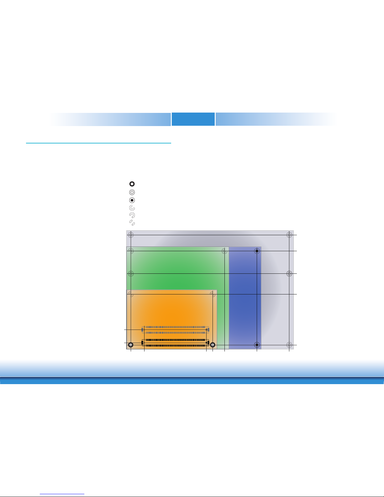
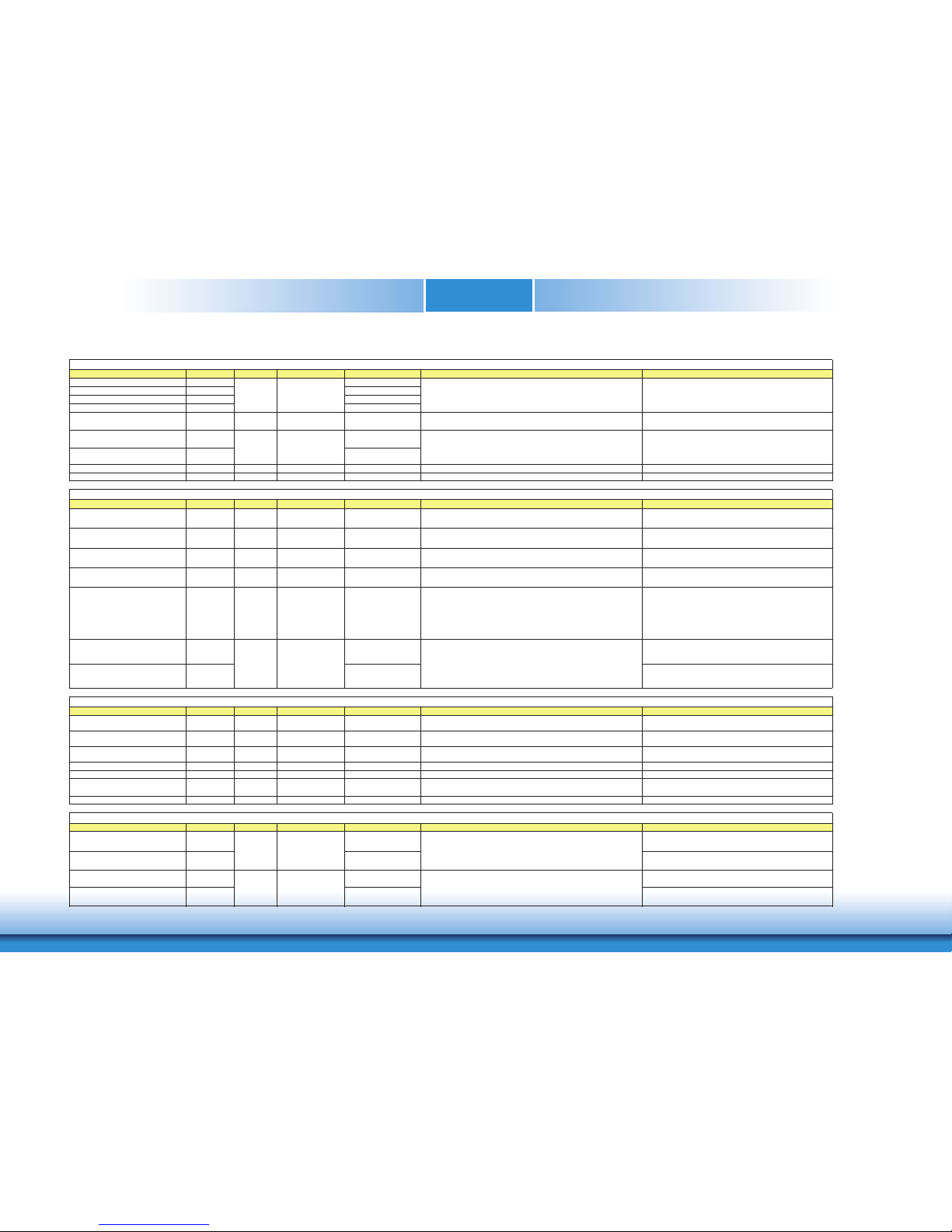
COM Express Module Standards
The figure below shows the dimensions of the different types of COM Express modules.
CH960-CM246/QM370/HM370 is a COM Express Basic module. Its dimension is 95mm x 125mm.
106.00
91.00
70.00
51.00
4.00
18.00
6.00
0.00
16.50
4.00
0.00
Extended
BasicCompact
Mini
74.20
80.00
91.00
121.00
151.00
Common for all Form Factors
Extended only
Basic only
Compact only
Compact and Basic only
Mini only
Page 9

www.dfi .comChapter 2 Concept
9
Chapter 2
Specification Comparison Table
• 5 Indicates 12V-tolerant features on former VCC_12V signals.
•
6
Cells in the connected columns spanning rows provide a rough approximation of features
sharing connector pins.
The table below shows the COM Express standard specifications and the corresponding specifications supported on the CH960-CM246/QM370/HM370 module.
Connector Feature
COM Express Module Base Specification
Type 6
(No IDE or PCI, add DDI+ USB3) Min / Max
DFI CH960
Type 6
A-B
A-B PCI Express Lanes 0 - 5 1 / 6 6
A-B LVDS Channel A 0 / 1 1
A-B LVDS Channel B 0 / 1 1
A-B eDP on LVDS CH A pins 0 / 1 1
A-B VGA Port 0 / 1 1
A-B TV-Out NA NA
A-B DDI 0 NA NA
A-B
5
Serial Ports 1 - 2 0 / 2 2
A-B CAN interface on SER1 0 / 1 0
A-B SATA / SAS Ports 1 / 4 4
A-B AC’97 / HDA Digital Interface 0 / 1 1
A-B USB 2.0 Ports 4 / 8 8
A-B USB Client 0 / 1 0
A-B USB 3.0 Ports NA NA
A-B LAN Port 0 1 / 1 1
A-B Express Card Support 1 / 2 2
A-B LPC Bus 1 / 1 1
A-B SPI 1 / 2 1
A-B
SDIO (muxed on GPIO) 0 / 1 NA
General Purpose I/O 8 / 8 8
A-B SMBus 1 / 1 1
A-B I2C 1 / 1 1
A-B Watchdog Timer 0 / 1 1
A-B Speaker Out 1 / 1 1
A-B External BIOS ROM Support 0 / 2 1
A-B Reset Functions 1 / 1 1
A-B
6
System I/O
System Management
Module Pin-out - Required and Optional Features C-D Connector.
Module Pin-out - Required and Optional Features A-B Connector.
Connector Feature
COM Express Module Base Specification
Type 6
(No IDE or PCI, add DDI+ USB3) Min / Max
DFI CH960
Type 6
A-B
A-B Thermal Protection 0 / 1 1
A-B Battery Low Alarm 0 / 1 1
A-B Suspend/Wake Signals 0 / 3 2
A-B Power Button Support 1 / 1 1
A-B Power Good 1 / 1 1
A-B VCC_5V_SBY Contacts 4 / 4 4
A-B
5
Sleep Input 0 / 1 1
A-B
5
Lid Input 0 / 1 1
A-B
5
Fan Control Signals 0 / 2 1
A-B Trusted Platform Modules 0 / 1 1 (optional)
A-B
A-B VCC_12V Contacts 12 / 12 12
Power Management
Power
Connector Feature
COM Express Module Base Specification
Type 6
(No IDE or PCI, add DDI+ USB3) Min / Max
DFI CH960
Type 6
C-D
PCI Express Lanes 16 - 31 0 / 16 16
PCI Express Graphics (PEG) 0 / 1 1
Muxed SDVO Channels 1 - 2 NA NA
PCI Express Lanes 6 - 15 0 / 2 2
PCI Bus - 32 Bit NA NA
PATA Port NA NA
LAN Ports 1 - 2 NA NA
DDIs 1 - 3 0 / 3 3 (DDI3 option)
USB 3.1 Ports 0 / 4 4
C-D
C-D VCC_12V Contacts 12 / 12 12
Power
C-D
6
C-D
6
System I/O
qp
Page 10
www.dfi .comChapter 3 Hardware Installation
10
Chapter 3
Chapter 3 - Hardware Installation
Board Layout
Top View
Bottom View
SPI Flash BIOS
BGA 1440
Core
Intel
CPU fan
Standby Power LED
Intel
CM246/QM370/HM370
DDR4_1 SODIMM
DDR4_2 SODIMM
Standby
Power LED
CPU fan
1
Intel
I219LM
CH7517
PTN3460
D110
D1
C110
C1
B110
B1
TPM (optional)
iTE
IT8528E
A110
A1
COM Express Connector
COM Express Connector
Page 11
www.dfi .comChapter 3 Hardware Installation
11
Chapter 3
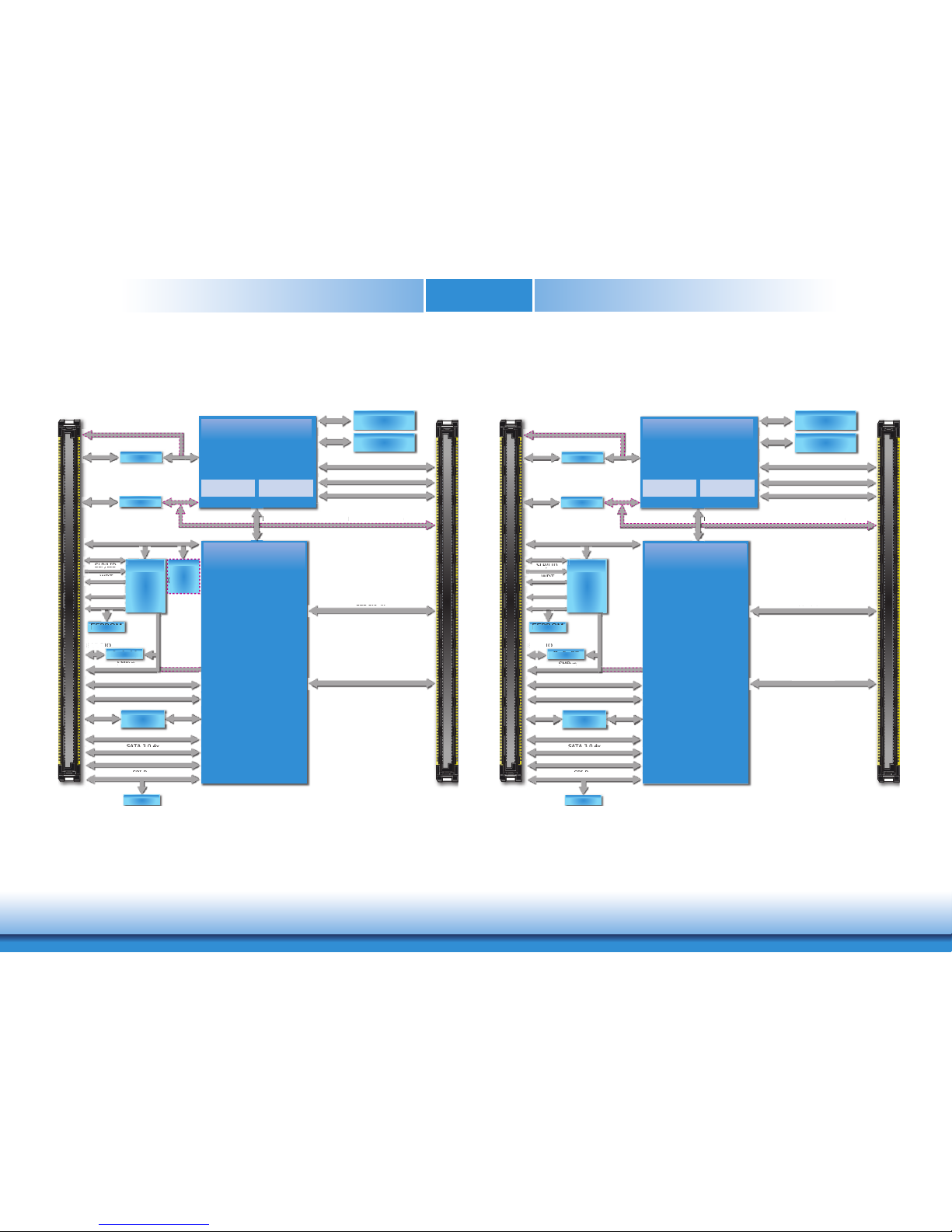
Block Diagram
Mobile
Intel
®
HM370
Chipset
USB 3.0 4x
Processor
2x Graphics
CORES
Memory
Controller
A / B
8th Generation
Intel
®
Core™ i7 (6 CORE)
DMI
DDI Port 1
USB 3.0 4x
PCIe (2 x1/1 x2)
C / D
PCIe (2 x1/1 x2)
DDR4 2666MHz
SODIMM
Channel A
DDR4 2666MHz
SODIMM
Channel B
DDI Port 2
EEPROM
SMBus
LPC Bus
LPC Bus
8-bit DIO
WDT
I
2
C Bus
Serial Port 0,1
Fan PWM/
TACH_IN
SLP/LID
SLP/LID
TCA6408A
Embedded
Controller
IT8528E
,
EEPROM
SMBus
t DIO8
O
TCA6408A
SPI Flash
SPI Bus
SATA 3.0 4x
SATA 3.0 4x
Intel®GLAN
I219LM
MDI
PCIe x1
PCIe (4 x1/1 x4)
PCIe (4 x1/1 x4)
HDA
HDA
USB 2.0 8x
USB 2.0 8x
DDI Port 3 (optional)
PCIe x16 (PEG)
CH7517
VGA
PCIe (2 x1/1 x2)
PCIe
(2
x1/1
x2)
D
MI
D
DI Port 3 (optional
)
D
eDP
PTN3460
LVDS
(optional)
8th Generation
Intel
®
Core™ i5/i3 (4 CORE)
Mobile
Intel
®
CM246/QM370
Chipset
USB 3.1 4x
Processor
2x Graphics
CORES
Memory
Controller
A / B
8th Generation
Intel
®
Xeon® E3 / Core™ i7 (6 CORE)
DMI
DDI Port 1
USB 3.1 4x
PCIe (2 x1/1 x2)
C / D
PCIe (2 x1/1 x2)
DDR4 2666MHz
SODIMM
Channel A
DDR4 2666MHz
SODIMM
Channel B
DDI Port 2
EEPROM
SMBus
LPC Bus
LPC Bus
8-bit DIO
WDT
I
2
C Bus
TPM 1.2/2.0
(optional)
Serial Port 0,1
Fan PWM/
TACH_IN
SLP/LID
SLP/LID
TCA6408A
T
T
(
Embedded
Controller
IT8528E
,
EEPROM
SMBus
t DIO8
O
TCA
640
8A
SPI Flash
SPI Bus
SATA 3.0 4x
SATA 3.0 4x
Intel®GLAN
I219LM
MDI
PCIe x1
PCIe (4 x1/1 x4)
PCIe(4x1/1
x4)
HDA
HDA
USB 2.0 8x
USB 2.0 8x
DDI Port 3 (optional)
PCIe x16 (PEG)
CH7517
VGA
PCIe (2 x1/1 x2)
PCIe (2 x1/1 x2)
D
MI
D
DI Port
3 (
opti
onal
)
D
eDP
PTN3460
LVDS
(optional)
8th Generation
Intel
®
Core™ i5/i3 (4 CORE)
CH960-HM370
CH960-CM246/QM370
Page 12

Chapter 3 Hardware Installation
12
Chapter 3
CPU fan
Standby Power LED
System Memory
DDR4_2
Standby
Power LED
DDR4_1
Important:
Electrostatic discharge (ESD) can damage your board, processor, disk drives, add-in
boards, and other components. Perform installation procedures at an ESD workstation
only. If such a station is not available, you can provide some ESD protection by wearing an antistatic wrist strap and attaching it to a metal part of the system chassis. If
a wrist strap is unavailable, establish and maintain contact with the system chassis
throughout any procedures requiring ESD protection.
Important:
When the Standby Power LED is red, it indicates that there is power on the board.
Power off the PC then unplug the power cord prior to installing any devices. Failure to
do so will cause severe damage to the board and components.
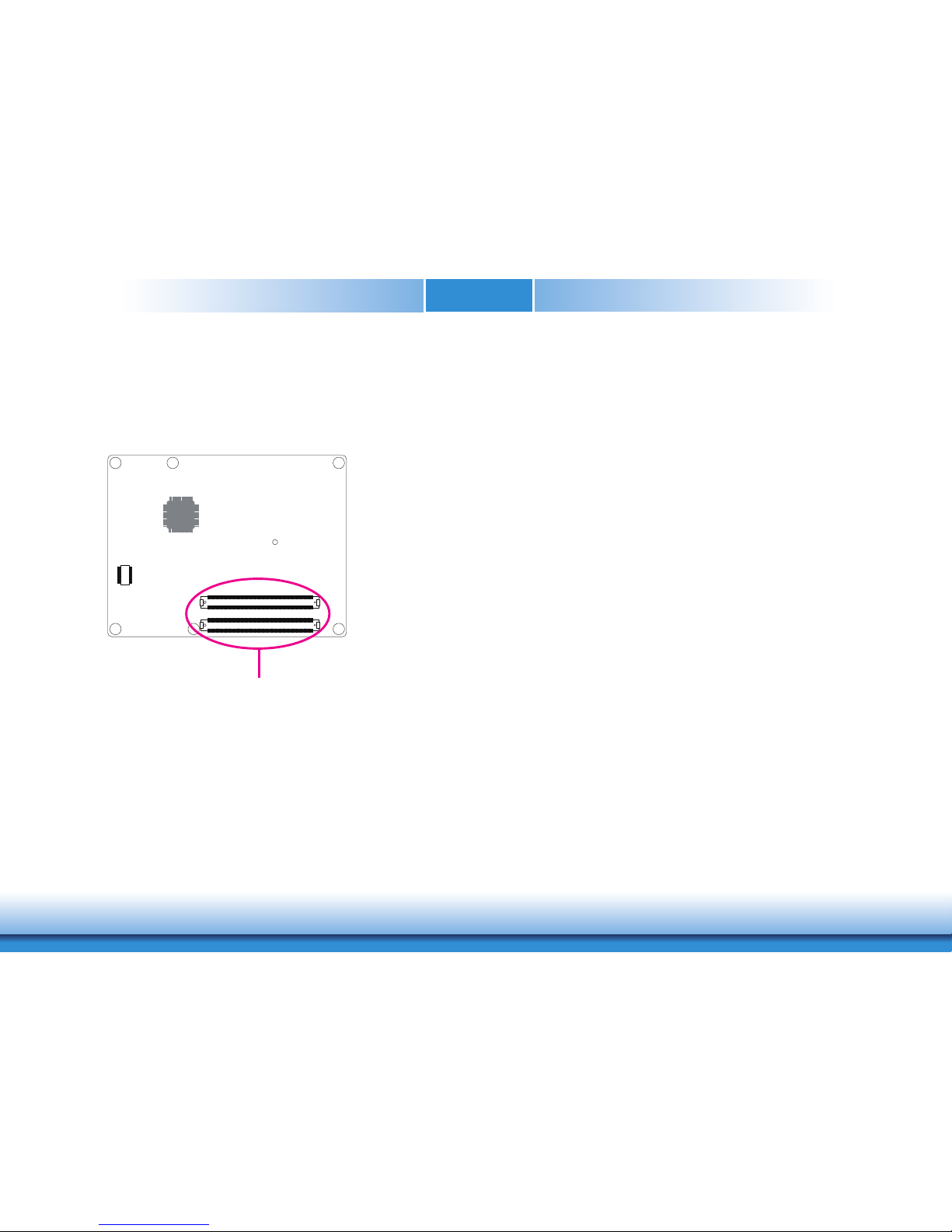
Installing the SODIMM Module
1. Make sure the PC and all other peripheral devices connected to it has been powered down.
2. Disconnect all power cords and cables.
3. Locate the SODIMM socket on the system board.
4. Note the key on the socket. The key ensures that the module can be plugged into the
socket in only one direction.
Note:
The system board used in the following illustrations may not resemble the actual one.
These illustrations are for reference only.
Page 13

www.dfi .comChapter 3 Hardware Installation
13
Chapter 3
CPU fan
Standby Power LED
Connectors
CPU Fan Connector
Connect the CPU fan’s cable connector to the CPU fan connector on the board. The cooling fan
will provide adequate airflow throughout the chassis to prevent overheating the CPU and board
components.
BIOS Setting
Configure the speed of the CPU fan in the “PC Health Status” submenu in the Advanced menu
of the BIOS.
3
1
Sense
+12V
Ground
6. Push down the module until the clips at each end of the socket lock into position. You will
hear a distinctive “click”, indicating the module is correctly locked into position.
Clip
Clip
5. Grasping the module by its edges, align the module into the socket at an approximately 30
degrees angle. Apply firm even pressure to each end of the module until it slips down into
the socket. The contact fingers on the edge of the module will almost completely disappear
inside the socket.
Page 14
www.dfi .comChapter 3 Hardware Installation
14
Chapter 3
COM Express Connectors
The COM Express connectors are used to interface the CH960-CM246/QM370/HM370 COM
Express board to a carrier board. Connect the COM Express connectors (located on the solder
side of the board) to the COM Express connectors on the carrier board.
Refer to the “Installing CH960-CM246/QM370/HM370 onto a Carrier Board” section for more
information.
COM Express Connectors
Refer to the following page for the pin functions of these connectors.
Page 15

www.dfi .comChapter 3 Hardware Installation
15
Chapter 3
COM Express Connectors-Continued
A1 GND (FIXED) B1 GND (FIXED) A56 PCIE_TX4- B56 PCIE_RX4- C1 GND (FIXED) D1 GND (FIXED) C56 PEG_RX1- D56 PEG_TX1A2 GBE0_MDI3- B2 GBE0_ACT# A57 GND B57 GPO2 C2 GND D2 GND C57 NC D57 GND
A3 GBE0_MDI3+ B3 LPC_FRAME# A58 PCIE_TX3+ B58 PCIE_RX3+ C3 USB_SSRX0- D3 USB_SSTX0- C58 PEG_RX2+ D58 PEG_TX2+
A4 GBE0_LINK100# B4 LPC_AD0 A59 PCIE_TX3- B59 PCIE_RX3- C4 USB_SSRX0+ D4 USB_SSTX0+ C59 PEG_RX2- D59 PEG_TX2A5 GBE0_LINK1000# B5 LPC_AD1 A60 GND (FIXED) B60 GND (FIXED) C5 GND D5 GND C60 GND (FIXED) D60 GND (FIXED)
A6 GBE0_MDI2- B6 LPC_AD2 A61 PCIE_TX2+ B61 PCIE_RX2+ C6 USB_SSRX1- D6 USB_SSTX1- C61 PEG_RX3+ D61 PEG
_TX3+
A7 GBE0_MDI2+ B7 LPC_AD3 A62 PCIE_TX2- B62 PCIE_RX2- C7 USB_SSRX1+ D7 USB_SSTX1+ C62 PEG_RX3- D62 PEG_TX3A8 GBE0_LINK# B8 LPC_DRQ0# A63 GPI1 B63 GPO3 C8 GND D8 GND C63 RSVD D63 RSVD
A9 GBE0_MDI1- B9 LPC_DRQ1# A64 PCIE_TX1+ B64 PCIE_RX1+ C9 USB_SSRX2- D9 USB_SSTX2- C64 RSVD D64 RSVD
A10 GBE0_MDI1+ B10 LPC_CLK A65 PCIE_TX1- B65 PCIE_RX1- C10 USB_SSRX2+ D10 USB_SSTX2+ C65 PEG_RX4+ D65 PEG_TX4+
A11 GND (FIXED) B11 GND (FIXED) A66 GND B66 WAKE0# C11 GND (FIXED) D11 GND (FIXED) C66 PEG_RX4- D66 PEG_TX4A12 GBE0_MDI0- B12 PWRBTN# A67 GPI2 B67 WAKE1# C12 USB_SSRX3- D12 USB_SSTX3- C67 RSVD D67 GND
A13 GBE0_MDI0+ B13 SMB_CK A68 PCIE_TX0+ B68 PCIE_RX0+ C13 USB_SSRX3+ D13 USB_SSTX3+ C68 PEG_RX5+ D68 PEG_TX5+
A14 NC B14 SMB_DAT A69 PCIE_TX0- B69 PCIE_RX0- C14 GND D14 GND C69 PEG_RX5- D69 PEG_TX5-
A15 SUS_S3# B15 SMB_ALERT# A70 GND (FIXED) B70 GND (FIXED) C15 NA, no support D15 DDI1_CTRLCLK_AUX+ C70 GND (FIXED) D70 GND (FIXED)
A16 SATA0_TX+ B16 SATA1_TX+ A71 LVDS_A0+/eDP_TX2+ B71 LVDS_B0+ C16 NA, no support D16 DDI1_CTRLDATA_AUX- C71 PEG_RX6+ D71 PEG_TX6+
A17 SATA0_TX- B17 SATA1_TX- A72 LVDS_A0-/eDP_TX2- B72 LVDS_B0- C17 RSVD D17 RSVD C72 PEG_RX6- D72 PEG_TX6A18 SUS_S4# B18 SUS_STAT# A73 LVDS_A1+/eDP_TX1+ B73 LVDS_B1+ C18 RSVD D18 RSVD C73 GND D73 GND
A19 SATA0_RX+ B19 SATA1_RX+ A74 LVDS_A1-/eDP_TX1- B74 LVDS_B1- C19 PCIE_RX6+ D19 PCIE_TX6+ C74 PEG_RX7+ D74 PEG_TX7+
A20 SATA0_RX- B20 SATA1_RX- A75 LVDS_A2+/eDP_TX0+ B75 LVDS_B2+ C20 PCIE_RX6- D20 PCIE_TX6- C75 PEG_RX7- D75 PEG_TX7A21 GND (FIXED) B21 GND (FIXED) A76 LVDS_A2-/eDP_TX0- B76 LVDS_B2- C21 GND (FIXED) D21 GND (FIXED) C76 GND D76 GND
A22 SATA2_TX+ B22 SATA3_TX+ A77 LVDS_VDD_EN/eDP_VDD_EN B77 LVDS_B3+ C22 PCIE_RX7+ D22 PCIE_TX7+ C77 RSVD D77 RSVD
A23 SATA2_TX- B23 SATA3_TX- A78 LVDS_A3+ B78 LVDS_B3- C23 PCIE_RX7- D23 PCIE_TX7- C78 PEG_RX8+ D78 PEG_TX8+
A24 SUS_S5# B24 PWR_OK A79 LVDS_A3- B79 LVDS_BKLT_EN/eDP_BKLT_EN C24 DDI1_HPD D24 RSVD C79 PEG_RX8- D79 PEG_TX8A25 SATA2_RX+ B25 SATA3_RX+ A80 GND (FIXED) B80 GND (FIXED) C25 NA, no support D25 RSVD C80 GND (FIXED) D80 GND (FIXED)
A26 SATA2_RX- B26 SATA3_RX- A81 LVDS_A_CK+/eDP_TX3+ B81 LVDS_B_CK+ C26 NA, no support D26 DDI1_PAIR0+ C81 PEG_RX9+ D81 PEG_TX9+
A27 BATLOW# B27 WDT A82 LVDS_A_CK-/eDP_TX3- B82 LVDS_B_CK- C27 RSVD D27 DDI1_PAIR0- C82 PEG_RX9- D82 PEG_TX9A28 (S)ATA_ACT# B28 NC A83 LVDS_I2C_CK/eDP_AUX+ B83 LVDS_BKLT_CTRL/eDP_BKLT_CTRL C28 RSVD D28 RSVD C83 RSVD D83 RSVD
A29 AC/HDA_SYNC B29 AC/HDA _SDIN1 A84 LVDS_I2C_DAT/eDP_AUX- B84 VCC_5V_SBY C29 NA, no support D29 DDI1_PAIR1+ C84 GND D84 GND
A30 AC/HDA _RST# B30 AC/HDA _SDIN0 A85 GPI3 B85 VCC_5V_SBY C30 NA, no support D30 DDI1_PAIR1- C85 PEG_RX10+ D85 PEG_TX10+
A31 GND (FIXED) B31 GND (FIXED) A86 RSVD B86 VCC_5V_SBY C31 GND (FIXED) D31 GND (FIXED) C86 PEG_RX10- D86 PEG_TX10A32 AC/HDA _BITCLK B32 SPKR A87 RSVD/eDP_HPD B87 VCC_5V_SBY C32 DDI2_CTRLCLK_AUX+ D32 DDI1_PAIR2+ C87 GND D87 GND
A33 AC/HDA _SDOUT B33 I2C_CK A88 PCIE0_CLK_REF+ B88 BIOS_DIS1# C33 DDI2_CTRLDATA_AUX- D33 DDI1_PAIR2- C88 PEG_RX11+ D88 PEG_TX11+
A34 BIOS_DIS0# B34 I2C_DAT A89 PCIE0_CLK_REF- B89 VGA_RED C34 DDI2_DDC_AUX_SEL D34 DDI1_DDC_AUX_SEL C89 PEG_RX11- D89 PEG_TX11A35 THRMTRIP# B35 THRM# A90 GND (FIXED) B90 GND (FIXED) C35 RSVD D35 RSVD C90 GND (FIXED) D90 GND (FIXED)
A36 USB6- B36 USB7- A91 SPI_POWER B91 VGA_GRN C36 DDI3_CTRLCLK_AUX+ D36 DDI1_PAIR3+ C91 PEG_RX12+ D91 PEG_TX12+
A37 USB6+ B37 USB7+ A92 SPI_MISO B92 VGA_BLU C37 DDI3_CTRLDATA_AUX- D37 DDI1_PAIR3- C92 PEG_RX12- D92 PEG_TX12A38 USB_6_7_OC# B38 USB_4_5_OC# A93 GPO0 B93 VGA_HSYNC C38 DDI3_DDC_AUX_SEL D38 RSVD C93 GND D93 GND
A39 USB4- B39 USB5- A94 SPI_CLK B94 VGA_VSYNC C39 DDI3_PAIR0+ D39 DDI2_PAIR0+ C94 PEG_RX13+ D94 PEG_TX13+
A40 USB4+ B40 USB5+ A95 SPI_MOSI B95 VGA_I2C_CK C40 DDI3_PAIR0- D40 DDI2_PAIR0- C95 PEG_RX13- D95 PEG_TX13A41 GND (FIXED) B41 GND (FIXED) A96 TPM_PP B96 VGA_I2C_DAT C41 GND (FIXED) D41 GND (FIXED) C96 GND D96 GND
A42 USB2- B42 USB3- A97 NC B97 SPI_CS# C42 DDI3_PAIR1+ D42 DDI2_PAIR1+ C97 RSVD D97 RSVD
A43 USB2+ B43 USB3+ A98 SER0_TX B98 RSVD C43 DDI3_PAIR1- D43 DDI2_PAIR1- C98 PEG_RX14+ D98 PEG_TX14+
A44 USB_2_3_OC# B44 USB_0_1_OC# A99 SER0_RX B99 RSVD C44 DDI3_HPD D44 DDI2_HPD C99 PEG_RX14- D99 PEG_TX14A45 USB0- B45 USB1- A100 GND (FIXED) B100 GND (FIXED) C45 RSVD D45 RSVD C100 GND (FIXED) D100 GND (FIXED)
A46 USB0+ B46 USB1+ A101 SER1_TX B101 FAN_PWMOUT C46 DDI3_PAIR2+ D46 DDI2_PAIR2+ C101 PEG_RX15+ D101 PEG_TX15+
A47 VCC_RTC B47 EXCD1_PERST# A102 SER1_RX B102 FAN_TACHIN C47 DDI3_PAIR2- D47 DDI2_PAIR2- C102 PEG_RX15- D102 PEG_TX15A48 EXCD0_PERST# B48 EXCD1_CPPE# A103 LID# B103 SLEEP# C48 RSVD D48 RSVD C103 GND D103 GND
A49 EXCD0_CPPE# B49 SYS_RESET# A104 VCC_12V B104 VCC_12V C49 DDI3_PAIR3+ D49 DDI2_PAIR3+ C104 VCC_12V D104 VCC_12V
A50 LPC_SERIRQ B50 CB_RESET# A105 VCC_12V B105 VCC_12V C50 DDI3_PAIR3- D50 DDI2_PAIR3- C105 VCC_12V D105 VCC_12V
A51 GND (FIXED) B51 GND (FIXED) A106 VCC_12V B106 VCC_12V C51 GND (FIXED) D51 GND (FIXED) C106 VCC_12V D106 VCC_12V
A52 PCIE_TX5+ B52 PCIE_RX5+ A107 VCC_12V B107 VCC_12V C52 PEG_RX0+ D52 PEG_TX0+ C107 VCC_12V D107 VCC_12V
A53 PCIE_TX5- B53 PCIE_RX5- A108 VCC_12V B108 VCC_12V C53 PEG_RX0- D53 PEG_TX0- C108 VCC_12V D108 VCC_12V
A54 GPI0 B54 GPO1 A109 VCC_12V B109 VCC_12V C54 NC D54 PEG_LANE_RV# C109 VCC_12V D109 VCC_12V
A55 PCIE_TX4+ B55 PCIE_RX4+ A110 GND (FIXED) B110 GND (FIXED) C55 PEG_RX1+ D55 PEG_TX1+ C110 GND (FIXED) D110 GND (FIXED)
Row C Row DRow A Row B Row C Row DRow A Row B
Page 16
www.dfi .comChapter 3 Hardware Installation
16
Chapter 3
COM Express Connectors Signals and Descriptions
Signal Pin# Pin Type Pwr Rail /Tolerance CH960 PU/PD Module Base Specification R2.1 Description COM Express Carrier Design Guide R2.0 Description
AC/HDA_RST# A30 O CMOS 3.3V Suspend/3.3V series 33 ɏ
resistor Reset output to CODEC, active low. CODEC Reset.
AC/HDA_SYNC A29 O CMOS 3.3V/3.3V series 33ɏ
resistor Sample-synchronization signal to the CODEC(s). Serial Sample Rate Synchronization.
AC/HDA_BITCLK A32 I/O CMOS 3.3V/3.3V series 33ɏ resistor Serial data clock generated by the external CODEC(s). 24 MHz Serial Bit Clock for HDA CODEC.
AC/HDA_SDOUT A33 O CMOS 3.3V/3.3V series 33ɏ
resistor Serial TDM data output to the CODEC. Audio Serial Data Output Stream.
AC/HDA_SDIN0 B30 I/O CMOS 3.3V Suspend/3.3V
AC/HDA_SDIN1 B29 I/O CMOS 3.3V Suspend/3.3V
AC/HDA_SDIN2 B28 I/O CMOS 3.3V Suspend/3.3V NC
Signal Pin# Pin Type Pwr Rail /Tolerance CH960 PU/PD Module Base Specification R2.1 Description COM Express Carrier Design Guide R2.0 Description
GBE0_MDI0+ A13 I/O Analog 3.3V max Suspend
GBE0_MDI0- A12 I/O Analog 3.3V max Suspend
GBE0_MDI1+ A10 I/O Analog 3.3V max Suspend
GBE0_MDI1- A9 I/O Analog 3.3V max Suspend
GBE0_MDI2+ A7 I/O Analog 3.3V max Suspend
GBE0_MDI2- A6 I/O Analog 3.3V max Suspend
GBE0_MDI3+ A3 I/O Analog 3.3V max Suspend
GBE0_MDI3-
A
2I
/
O Analog3.3V max Suspend
GBE0_ACT# B2 OD CMO
S
3.3V Suspend/3.3V Gigabit Ethernet Controller 0 activity indicator, active low. Ethernet controller 0 activity indicator, active low.
GBE0_LINK# A8 OD CMOS 3.3V Suspend/3.3V Gigabit Ethernet Controller 0 link indicator, active low. Ethernet controller 0 link indicator, active low.
GBE0_LINK100#
A
4OD CMOS3.3V Suspend/3.3V Gigabit Ethernet Controller 0 100 Mbit / sec link indicator, active low. Ethernet controller 0 100Mbit/sec link indicator, active low.
GBE0_LINK1000#
A
5OD CMOS3.3V Suspend/3.3V Gigabit Ethernet Controller 0 1000 Mbit / sec link indicator, active low. Ethernet controller 0 1000Mbit/sec link indicator, active low.
GBE0_CTREF A14 REF GND min 3.3V max NC
Reference voltage for Carrier Board Ethernet channel 0 magnetics center
tap. The reference voltage is determined by the requirements of the
Module PHY and may be as low as 0V and as high as 3.3V.
The reference voltage output shall be current limited on the Module. In
the case in which the reference is shorted to ground, the current shall be
limited to 250 mA or less.
Reference voltage for Carrier Board Ethernet channel 0
magnetics center tap.
Signal Pin# Pin Type Pwr Rail /Tolerance CH960 PU/PD Module Base Specification R2.1 Description COM Express Carrier Design Guide R2.0 Description
SATA0_TX+ A16 O SATA AC coupled on Module AC Coupling capacitor
SATA0_TX- A17 O SATA AC coupled on Module AC Coupling capacitor
SATA0_RX+ A19 I SATA AC coupled on Module AC Coupling capacitor
SATA0_RX- A20 I SATA AC coupled on Module AC Coupling capacitor
SATA1_TX+ B16 O SATA AC coupled on Module AC Coupling capacitor
SATA1_TX- B17 O SATA AC coupled on Module AC Coupling capacitor
SATA1_RX+ B19 I SATA AC coupled on Module AC Coupling capacitor
SATA1_RX- B20 I SATA AC coupled on Module AC Coupling capacitor
SATA2_TX+ A22 O SATA AC coupled on Module AC Coupling capacitor
SATA2_TX- A23 O SATA AC coupled on Module AC Coupling capacitor
SATA2_RX+ A25 I SATA AC coupled on Module AC Coupling capacitor
SATA2_RX- A26 I SATA AC coupled on Module AC Coupling capacitor
SATA3_TX+ B22 O SATA AC coupled on Module AC Coupling capacitor
SATA3_TX- B23 O SATA AC coupled on Module AC Coupling capacitor
SATA3_RX+ B25 I SATA AC coupled on Module AC Coupling capacitor
SATA3_RX- B26 I SATA AC coupled on Module AC Coupling capacitor
(S)ATA_ACT# A28 I/O CMOS 3.3V / 3.3V PU 10K: to 3.3V ATA (parallel and serial) or SAS activity indicator, active low.
Serial ATA activit
y
LED. Open collector output pin driven durin
g
SATA command activity.
Pin Types
I Input to the Module
O Output from the Module
I/O Bi-directional input / output signal
OD Open drain output
RSVD pins are reserved for future use and should be no connect. Do not tie the RSVD pins together.
Serial ATA channel 2
Transmit output differential pair.
Serial ATA channel 0
Transmit output differential pair.
Serial ATA channel 0
Receive input differential pair.
Serial ATA channel 1
Transmit output differential pair.
Serial ATA channel 3
Receive input differential pair.
Serial ATA channel 2
Receive input differential pair.
Serial ATA channel 3
Transmit output differential pair.
A
C97/HDA Signals Description
s
Serial TDM data inputs from up to 3 CODECs.
Gigabit Ethernet Signals Description
s
Serial ATA or SAS Channel 0 transmit differential pair.
Serial ATA or SAS Channel 0 receive differential pair.
Serial ATA or SAS Channel 3 transmit differential pair.
Serial ATA or SAS Channel 3 receive differential pair.
Serial ATA or SAS Channel 2 receive differential pair.
Serial ATA or SAS Channel 2 transmit differential pair.
Gigabit Ethernet Controller 0: Media Dependent Interface Differential
Pairs 0,1,2,3. The MDI can operate in 1000, 100 and 10 Mbit / sec
modes. Some pairs are unused in some modes, per the following:
1000BASE-T 100BASE-TX 10BASE-T
MDI[0]+/- B1_DA+/- TX+/- TX+/ MDI[1]+/- B1_DB+/- RX+/- RX+/ MDI[2]+/- B1_DC+/ MDI[3]+/- B1_DD+/-
Serial ATA or SAS Channel 1 receive differential pair.
SATA Signals Description
s
Serial ATA or SAS Channel 1 transmit differential pair.
Audio Serial Data Input Stream from CODEC[0:2].
Media Dependent Interface (MDI) differential pair 0.
Media Dependent Interface (MDI) differential pair 1.
Media Dependent Interface (MDI) differential pair 2.
Only used for 1000Mbit/sec Gigabit Ethernet mode.
Media Dependent Interface (MDI) differential pair 3.
Only used for 1000Mbit/sec Gigabit Ethernet mode.
Serial ATA channel 1
Receive input differential pair.
Page 17
www.dfi .comChapter 3 Hardware Installation
17
Chapter 3
Signal Pin# Pin Type Pwr Rail /Tolerance CH960 PU/PD Module Base Specification R2.1 Description COM Express Carrier Design Guide R2.0 Description
PCIE_TX0+ A68 AC Coupling capacitor
PCIE_TX0- A69 AC Coupling capacitor
PCIE_RX0+ B68
PCIE_RX0- B69
PCIE_TX1+ A64 AC Coupling capacitor
PCIE_TX1- A65 AC Coupling capacitor
PCIE_RX1+ B64
PCIE_RX1- B65
PCIE_TX2+ A61 AC Coupling capacitor
PCIE_TX2- A62 AC Coupling capacitor
PCIE_RX2+ B61
PCIE_RX2- B62
PCIE_TX3+ A58 AC Coupling capacitor
PCIE_TX3- A59 AC Coupling capacitor
PCIE_RX3+ B58
PCIE_RX3- B59
PCIE_TX4+ A55 AC Coupling capacitor
PCIE_TX4- A56 AC Coupling capacitor
PCIE_RX4+ B55
PCIE_RX4- B56
PCIE_TX5+ A52 AC Coupling capacitor
PCIE_TX5- A53 AC Coupling capacitor
PCIE_RX5+ B52
PCIE_RX5- B53
PCIE_TX6+ D19 AC Coupling capacitor
PCIE_TX6- D20 AC Coupling capacitor
PCIE_RX6+ C19
PCIE_RX6- C20
PCIE_TX7+ D22 AC Coupling capacitor
PCIE_TX7- D23 AC Coupling capacitor
PCIE_RX7+ C22
PCIE_RX7- C23
PCIE_CLK_REF+ A88
PCIE_CLK_REF- A89
Signal Pin# Pin Type Pwr Rail /Tolerance CH960 PU/PD Module Base Specification R2.1 Description COM Express Carrier Design Guide R2.0 Description
PEG_TX0+ D52 AC Coupling capacitor
PEG_TX0- D53 AC Coupling capacitor
PEG_RX0+ C52
PEG_RX0- C53
PEG_TX1+ D55 AC Coupling capacitor
PEG_TX1- D56 AC Coupling capacitor
PEG_RX1+ C55
PEG_RX1- C56
PEG_TX2+ D58 AC Coupling capacitor
PEG_TX2- D59 AC Coupling capacitor
PEG_RX2+ C58
PEG_RX2- C59
PEG_TX3+ D61 AC Coupling capacitor
PEG_TX3- D62 AC Coupling capacitor
PEG_RX3+ C61
PEG_RX3- C62
PEG_TX4+ D65 AC Coupling capacitor
PEG_TX4- D66 AC Coupling capacitor
PEG_RX4+ C65
PEG_RX4- C66
PEG_TX5+ D68 AC Coupling capacitor
PEG_TX5- D69 AC Coupling capacitor
PEG_RX5+ C68
PEG_RX5- C69
PCIe channel 4. Receive Input differential pair.
PCIe channel 5. Transmit Output differential pair.
PCIe channel 6. Transmit Output differential pair.
PCIe channel 6. Receive Input differential pair.
PCIe channel 7. Transmit Output differential pair.
PCIe channel 7. Receive Input differential pair.
PCIe Reference Clock for all COM Express PCIe lanes, and for
PEG lanes.
PEG channel 5, Receive Input differential pair.I PCIE AC coupled off Module PCI Express Graphics receive differential pairs 5
PEG channel 5, Transmit Output differential pair.O PCIE AC coupled on Module
PCI Express Graphics transmit differential pairs 4
I PCIE AC coupled off Module
I PCIE AC coupled off Module PCI Express Graphics receive differential pairs 3
PCI Express Graphics transmit differential pairs 5
I PCIE AC coupled off Module PCI Express Graphics receive differential pairs 2
O PCIE AC coupled on Module PCI Express Graphics transmit differential pairs 3
PCI Express Graphics receive differential pairs 4
O PCIE AC coupled on Module
PEG channel 2, Receive Input differential pair.
PEG channel 3, Transmit Output differential pair.
PEG channel 3, Receive Input differential pair.
PEG channel 4, Transmit Output differential pair.
PEG channel 4, Receive Input differential pair.
PCI Express Graphics transmit differential pairs 2
PEG Signals Description
s
O PCIE AC coupled on Module PCI Express Graphics transmit differential pairs 0
I PCIE AC coupled off Module PCI Express Graphics receive differential pairs 0
O PCIE AC coupled on Module PCI Express Graphics transmit differential pairs 1
AC coupled off Module PCI Express Graphics receive differential pairs 1
PEG channel 0, Transmit Output differential pair.
PEG channel 0, Receive Input differential pair.
PEG channel 1, Transmit Output differential pair.
PEG channel 1, Receive Input differential pair.
PEG channel 2, Transmit Output differential pair.O PCIE AC coupled on Module
I PCIE
PCI Express Differential Receive Pairs 7
O PCIE PCIE Reference clock output for all PCI Express and PCI Express Graphics lanes.
PCI Express Differential Receive Pairs 6
O PCIE AC coupled on Module PCI Express Differential Transmit Pairs 7
PCI Express Differential Transmit Pairs 4
PCIe channel 5. Receive Input differential pair.
PCIe channel 4. Transmit Output differential pair.
I PCIE AC coupled off Module
I PCIE AC coupled off Module
O PCIE AC coupled on Module PCI Express Differential Transmit Pairs 6
I PCIE AC coupled off Module PCI Express Differential Receive Pairs 5
O PCIE AC coupled on Module PCI Express Differential Transmit Pairs 5
PCI Express Differential Receive Pairs 4
O PCIE AC coupled on Module
I PCIE AC coupled off Module
PCIe channel 3. Receive Input differential pair.
O PCIE AC coupled on Module PCI Express Differential Transmit Pairs 1
PCI Express Differential Receive Pairs 1
PCI Express Differential Receive Pairs 3
I PCIE AC coupled off Module PCI Express Differential Receive Pairs 2
PCI Express Differential Transmit Pairs 3O PCIE AC coupled on Module PCIe channel 3. Transmit Output differential pair.
PCIe channel 2. Transmit Output differential pair.
PCIe channel 2. Receive Input differential pair.
PCIe channel 1. Transmit Output differential pair.
PCIe channel 1. Receive Input differential pair.
I PCIE AC coupled off Module
O PCIE AC coupled on Module PCI Express Differential Transmit Pairs 0
O PCIE AC coupled on Module PCI Express Differential Transmit Pairs 2
I PCIE AC coupled off Module
I PCIE AC coupled off Module PCI Express Differential Receive Pairs 0
PCIe channel 0. Transmit Output differential pair.
PCIe channel 0. Receive Input differential pair.
PCI Express Lanes Signals Description
s
Page 18

www.dfi .comChapter 3 Hardware Installation
18
Chapter 3
Signal Pin# Pin Type Pwr Rail /Tolerance CH960 PU/PD Module Base Specification R2.1 Description COM Express Carrier Design Guide R2.0 Description
PEG Signals Description
s
PEG_TX6+ D71 AC Coupling capacitor
PEG_TX6- D72 AC Coupling capacitor
PEG_RX6+ C71
PEG_RX6- C72
PEG_TX7+ D74 AC Coupling capacitor
PEG_TX7- D75 AC Coupling capacitor
PEG_RX7+ C74
PEG_RX7- C75
PEG_TX8+ D78 AC Coupling capacitor
PEG_TX8- D79 AC Coupling capacitor
PEG_RX8+ C78
PEG_RX8- C79
PEG_TX9+ D81 AC Coupling capacitor
PEG_TX9- D82 AC Coupling capacitor
PEG_RX9+ C81
PEG_RX9- C82
PEG_TX10+ D85 AC Coupling capacitor
PEG_TX10- D86 AC Coupling capacitor
PEG_RX10+ C85
PEG_RX10- C86
PEG_TX11+ D88 AC Coupling capacitor
PEG_TX11- D89 AC Coupling capacitor
PEG_RX11+ C88
PEG_RX11- C89
PEG_TX12+ D91 AC Coupling capacitor
PEG_TX12- D92 AC Coupling capacitor
PEG_RX12+ C91
PEG_RX12- C92
PEG_TX13+ D94 AC Coupling capacitor
PEG_TX13- D95 AC Coupling capacitor
PEG_RX13+ C94
PEG_RX13- C95
PEG_TX14+ D98 AC Coupling capacitor
PEG_TX14- D99 AC Coupling capacitor
PEG_RX14+ C98
PEG_RX14- C99
PEG_TX15+ D101 AC Coupling capacitor
PEG_TX15- D102 AC Coupling capacitor
PEG_RX15+ C101
PEG_RX15- C102
PEG_LANE_RV# D54 I CMOS 3.3V / 3.3V PU 10Kɏ
to 3V3
PCI Express Graphics lane reversal input strap.
Pull low on the Carrier board to reverse lane order.
PCI Express Graphics lane reversal input strap.
Pull low on the carrier board to reverse lane order.
Signal Pin# Pin Type Pwr Rail /Tolerance CH960 PU/PD Module Base Specification R2.1 Description COM Express Carrier Design Guide R2.0 Description
EXCD0_CPPE# A49 I CMOS 3.3V /3.3V PU 10k to 3.3V
PCI Ex
p
ressCard: PCI Express capable card request, active low, one per
card
PCI ExpressCard0: PCI Express capable card request, active low,
one
p
er card
EXCD0_PERST#
A
48 O CMOS3.3V /3.3V PCI ExpressCard: reset, active low, one per card PCI ExpressCard0: reset, active low, one per card
EXCD1_CPPE# B48 I CMOS 3.3V /3.3V PU 10k to 3.3V PCI ExpressCard: PCI Express capable card request, active low, one percard
PCI Ex
p
ressCard1: PCI Express capable card request, active low,
one
p
er card
EXCD1_PERST# B47 O CMO
S
3.3V /3.3V PCI ExpressCard: reset, active low, one per card PCI ExpressCard1: reset, active low, one per card
Signal Pin# Pin Type Pwr Rail /Tolerance CH960 PU/PD Module Base Specification R2.1 Description COM Express Carrier Design Guide R2.0 Description
USB0+ A46 USB Port 0, data + or D+
USB0- A45 USB Port 0, data - or D-
USB1+ B46 USB Port 1, data + or D+
USB1- B45 USB Port 1, data - or D-
I PCIE
PEG channel 15, Transmit Output differential pair.
PCI Express Graphics transmit differential pairs 12
O PCIE AC coupled on Module PCI Express Graphics transmit differential pairs 11
PEG channel 15, Receive Input differential pair.
I PCIE AC coupled off Module
O PCIE AC coupled on Module
I/O USB
PEG channel 12, Transmit Output differential pair.
3.3V Suspend/3.3V USB differential pairs, channel 1
I PCIE AC coupled off Module
PCI Express Graphics receive differential pairs 14
PCI Express Graphics receive differential pairs 12
ExpressCard Signals Description
s
O PCIE AC coupled on Module PCI Express Graphics transmit differential pairs 14
I PCIE AC coupled off Module PCI Express Graphics receive differential pairs 15
PEG channel 12, Receive Input differential pair.
PEG channel 13 Transmit Output differential pair.
PEG channel 13, Receive Input differential pair.
USB Signals Description
s
I/O USB 3.3V Suspend/3.3V USB differential pairs, channel 0
PEG channel 14, Transmit Output differential pair.
PEG channel 14, Receive Input differential pair.
PEG channel 9, Transmit Output differential pair.
PEG channel 9, Receive Input differential pair.
PEG channel 10, Transmit Output differential pair.O PCIE AC coupled on Module
PCI Express Graphics receive differential pairs 13
O PCIE AC coupled on Module PCI Express Graphics transmit differential pairs 15
I PCIE AC coupled off Module
O PCIE AC coupled on Module PCI Express Graphics transmit differential pairs 13
AC coupled off Module
I PCIE AC coupled off Module PCI Express Graphics receive differential pairs 11
PCI Express Graphics receive differential pairs 10 PEG channel 10, Receive Input differential pair.
PEG channel 11, Transmit Output differential pair.
PEG channel 11, Receive Input differential pair.
O PCIE
O PCIE AC coupled on Module PCI Express Graphics transmit differential pairs 6
PCI Express Graphics transmit differential pairs 10
I PCIE AC coupled off Module PCI Express Graphics receive differential pairs 9
O PCIE AC coupled on Module PCI Express Graphics transmit differential pairs 9
PEG channel 6, Transmit Output differential pair.
PEG channel 6, Receive Input differential pair.
PEG channel 7, Transmit Output differential pair.
PEG channel 7, Receive Input differential pair.
PEG channel 8, Transmit Output differential pair.O PCIE AC coupled on Module
PCI Express Graphics receive differential pairs 8
I PCIE AC coupled off Module PCI Express Graphics receive differential pairs 7
AC coupled on Module PCI Express Graphics transmit differential pairs 7
I PCIE AC coupled off Module PCI Express Graphics receive differential pairs 6
PEG channel 8, Receive Input differential pair.I PCIE AC coupled off Module
PCI Express Graphics transmit differential pairs 8
Page 19

www.dfi .comChapter 3 Hardware Installation
19
Chapter 3
USB2+ A43 USB Port 2, data + or D+
USB2- A42 USB Port 2, data - or D-
USB3+ B43 USB Port 3, data + or D+
USB3- B42 USB Port 3, data - or D-
USB4+ A40 USB Port 4, data + or D+
USB4- A39 USB Port 4, data - or D-
USB5+ B40 USB Port 5, data + or D+
USB5- B39 USB Port 5, data - or D-
USB6+ A37 USB Port 6, data + or D+
USB6- A36 USB Port 6, data - or D-
USB7+ B37 USB Port 7, data + or D+
USB7- B36 USB Port 7, data - or D-
USB_0_1_OC# B44 I CMOS 3.3V Suspend/3.3V
PU 10K: to 3.3V
Suspend
USB over-current sense, USB channels 0 and 1. A pull-up for this line
shall be present on the Module. An open drain driver from a USB
current monitor on the Carrier Board may drive this line low. Do not
pull this line high on the Carrier Board.
USB over-current sense, USB ports 0 and 1.
USB_2_3_OC# A44 I CMOS 3.3V Suspend/3.3V
PU 10K: to 3.3V
Suspend
USB over-current sense, USB channels 2 and 3. A pull-up for this line
shall be present on the Module. An open drain driver from a USB
current monitor on the Carrier Board may drive this line low. Do not
pull this line high on the Carrier Board.
USB over-current sense, USB ports 2 and 3.
USB_4_5_OC# B38 I CMOS 3.3V Suspend/3.3V
PU 10K: to 3.3V
Suspend
USB over-current sense, USB channels 4 and 5. A pull-up for this line
shall be present on the Module. An open drain driver from a USB
current monitor on the Carrier Board may drive this line low. Do not
pull this line high on the Carrier Board.
USB over-current sense, USB ports 4 and 5.
USB_6_7_OC# A38 I CMOS 3.3V Suspend/3.3V
PU 10K: to 3.3V
Suspend
USB over-current sense, USB channels 6 and 7. A pull-up for this line
shall be present on the Module. An open drain driver from a USB
current monitor on the Carrier Board may drive this line low. Do not
pull this line high on the Carrier Board.
USB over-current sense, USB ports 6 and 7.
USB_SSTX0+ D4 AC Coupling capacitor USB Port 0, SuperSpeed TX +
USB_SSTX0- D3 AC Coupling capacitor USB Port 0, SuperSpeed TX -
USB_SSRX0+ C4 USB Port 0, SuperSpeed RX +
USB_SSRX0- C3 USB Port 0, SuperSpeed RX -
USB_SSTX1+ D7 AC Coupling capacitor USB Port 1, SuperSpeed TX +
USB_SSTX1- D6 AC Coupling capacitor USB Port 1, SuperSpeed TX -
USB_SSRX1+ C7 USB Port 1, SuperSpeed RX +
USB_SSRX1- C6 USB Port 1, SuperSpeed RX -
USB_SSTX2+ D10 AC Coupling capacitor USB Port 2, SuperSpeed TX +
USB_SSTX2- D9 AC Coupling capacitor USB Port 2, SuperSpeed TX -
O PCIE AC coupled on Module
Additional receive signal differential pairs for the SuperSpeed USB data
path.
I/O USB 3.3V Suspend/3.3V USB differential pairs, channel 2
Additional transmit signal differential pairs for the SuperSpeed USB data
path.
O PCIE AC coupled on Module
Additional transmit signal differential pairs for the SuperSpeed USB data
path.
I PCIE AC coupled off Module
O PCIE AC coupled on Module
Additional transmit signal differential pairs for the SuperSpeed USB data
path.
I/O USB 3.3V Suspend/3.3V USB differential pairs, channel 6
Additional receive signal differential pairs for the SuperSpeed USB data
path.
I PCIE AC coupled off Module
I/O USB 3.3V Suspend/3.3V USB differential pairs, channel 5
I/O USB 3.3V Suspend/3.3V
USB differential pairs, channel 7.
USB7 may be configured as a USB client or as a host, or both, at the
Module designer's discretion. (CH960 default set as a host)
3.3V Suspend/3.3V USB differential pairs, channel 4
I/O USB 3.3V Suspend/3.3V USB differential pairs, channel 3
I/O USB
Signal Pin# Pin Type Pwr Rail /Tolerance CH960 PU/PD Module Base Specification R2.1 Description COM Express Carrier Design Guide R2.0 Description
USB Signals Description
s
Page 20
www.dfi .comChapter 3 Hardware Installation
20
Chapter 3
USB_SSRX2+ C10 USB Port 2, SuperSpeed RX +
USB_SSRX2- C9 USB Port 2, SuperSpeed RX -
USB_SSTX3+ D13 AC Coupling capacitor USB Port 3, SuperSpeed TX +
USB_SSTX3- D12 AC Coupling capacitor USB Port 3, SuperSpeed TX -
USB_SSRX3+ C13 USB Port 3, SuperSpeed RX +
USB_SSRX3- C12 USB Port 3, SuperSpeed RX -
Signal Pin# Pin Type Pwr Rail /Tolerance CH960 PU/PD Module Base Specification R2.1 Description COM Express Carrier Design Guide R2.0 Description
LVDS_A0+/eDP_TX2+ A71
LVDS_A0-/eDP_TX2- A72
LVDS_A1+/eDP_TX1+ A73
LVDS_A1-/eDP_TX1- A74
LVDS_A2+/eDP_TX0+ A75
LVDS_A2-/eDP_TX0- A76
LVDS_A3+ A78
LVDS_A3- A79
LVDS_A_CK+/eDP_TX3+ A81
LVDS_A_CK-/eDP_TX3- A82
LVDS_B0+ B71
LVDS_B0- B72
LVDS_B1+ B73
LVDS_B1- B74
LVDS_B2+ B75
LVDS_B2- B76
LVDS_B3+ B77
LVDS_B3- B78
LVDS_B_CK+ B81
LVDS_B_CK- B82
LVDS_VDD_EN/eDP_VDD_EN A77 O CMOS 3.3V / 3.3V LVDS/eDP: PD 100K : LVDS panel power enable
LVDS flat panel power enable.
eDP power enable
LVDS_BKLT_EN/eDP_BKLT_EN B79 O CMOS 3.3V / 3.3V LVDS/eDP: PD 100K: LVDS panel backlight enable
LVDS flat panel backlight enable high active signal
eDP backlight enable
LVDS_BKLT_CTRL/eDP_BKLT_CTRL B83 O CMOS 3.3V / 3.3V LVDS/eDP: PD 100K : LVDS panel backlight brightness control
LVDS flat panel backlight brightness control
EDP backlight brightness control
LVDS_I2C_CK/eDP_AUX+ A83 I/O OD CMOS 3.3V / 3.3V PU 4.7K: to 3.3V I2C clock output for LVDS display use
DDC I2C clock signal used for flat panel detection and control.
eDP auxiliary lane +
LVDS_I2C_DAT/eDP_AUX- A84 I/O OD CMOS 3.3V / 3.3V PU 4.7K: to 3.3V I2C data line for LVDS display use
DDC I2C data signal used for flat panel detection and control.
eDP auxiliary lane -
RSVD/eDP_HPD A87 I CMOS 3.3V / 3.3V
LVDS: RSV series resistor
to PCH EDP HPD
eDP: Connect to PCH
EDP HPD w
/
PD 100K:
eDP_HPD:Detection of Hot Plug / Unplug and notification of the link layer
eDP_HPD: Detection of Hot Plug / Unplug and notification of the
link layer
O LVDS LVDS
O PCIE
I PCIE AC coupled off Module
LVDS
O LVDS LVDS
Additional receive signal differential pairs for the SuperSpeed USB data
path.
LVDS Signals Description
s
O LVDS
LVDS
EDP: AC coupled off
Module
LVDS channel A differential signal pair 0
eDP lane 2, TXƲ
differential signal pair
LVDS Channel A differential pairs
Ther LVDS flat panel differential pairs (LVDS_A[0:3]+/-, LVDS_B[0:3]+/-.
LVDS_A_CK+/-, LVDS_B_CK+/-) shall have 100ƻ terminations across the
pairs at the destination. These terminations may be on the Carrier Board if
the Carrier Board implements a LVDS deserializer on-board.
eDP: eDP differential pairs
O LVDS
LVDS channel A differential signal pair 1
eDP lane 1, TXƲ
differential signal pair
O LVDS
LVDS
EDP: AC coupled off
Module
LVDS channel A differential signal pair 3
LVDS
EDP: AC coupled off
Module
LVDS channel A differential signal pair 2
eDP lane 0, TX Ʋ
differential signal pair
O LVDS
LVDS
EDP: AC coupled off
Module
LVDS channel B differential signal pair 2
LVDS Channel A differential clockO LVDS LVDS
LVDS channel A differential clock pair
eDP lane 3, TXƲ
differential pair
O LVDS
LVDS channel B differential signal pair 0
LVDS channel B differential signal pair 1
LVDS Channel B differential clock
LVDS Channel B differential pairs
Ther LVDS flat panel differential pairs (LVDS_A[0:3]+/-, LVDS_B[0:3]+/-.
LVDS_A_CK+/-, LVDS_B_CK+/-) shall have 100ƻ terminations across the
pairs at the destination. These terminations may be on the Carrier Board if
the Carrier Board implements a LVDS deserializer on-board.
O LVDS LVDS LVDS channel B differential signal pair 3
O LVDS LVDS LVDS channel B differential clock pair
AC coupled on Module
Additional transmit signal differential pairs for the SuperSpeed USB data
path.
I PCIE AC coupled off Module
Additional receive signal differential pairs for the SuperSpeed USB data
path.
Signal Pin# Pin Type Pwr Rail /Tolerance CH960 PU/PD Module Base Specification R2.1 Description COM Express Carrier Design Guide R2.0 Description
USB Signals Description
s
Page 21
www.dfi .comChapter 3 Hardware Installation
21
Chapter 3
Signal Pin# Pin Type Pwr Rail /Tolerance CH960 PU/PD Module Base Specification R2.1 Description COM Express Carrier Design Guide R2.0 Description
LPC_AD0 B4
LPC_AD1 B5
LPC_AD2 B6
LPC_AD3 B7
LPC_FRAME# B3 O CMOS 3.3V / 3.3V LPC frame indicates the start of an LPC cycle
LPC frame indicates start of a new cycle or termination of a
broken cycle.
LPC_DRQ0# B8
PU 10K to 3.3V, not
support.
LPC_DRQ1# B9
PU 10K to 3.3V, not
support.
LPC_SERIRQ A50 I/O CMOS 3.3V / 3.3V PU 10K to 3.3V LPC serial interrupt LPC serialized IRQ.
LPC_CLK B10 O CMOS 3.3V / 3.3V series 22ƻ resistor LPC clock output - 33MHz nominal LPC clock output 33MHz.
Signal Pin# Pin Type Pwr Rail /Tolerance CH960 PU/PD Module Base Specification R2.1 Description COM Express Carrier Design Guide R2.0 Description
SPI_CS# B97 O CMOS 3.3V Suspend/3.3V
Chip select for Carrier Board SPI - may be sourced from chipset SPI0 or
SPI1
Chip select for Carrier Board SPI – may be sourced from chipset
SPI0 or SPI1
SPI_MISO A92 I CMOS 3.3V Suspend/3.3V Data in to Module from Carrier SPI
Data in to Module from Carrier SPI
SPI_MOSI A95 O CMOS 3.3V Suspend/3.3V Data out from Module to Carrier SPI
Data out from Module to Carrier SPI
SPI_CLK A94 O CMOS 3.3V Suspend/3.3V Clock from Module to Carrier SPI
Clock from Module to Carrier SPI
SPI_POWER A91 O 3.3V Suspend/3.3V
Power supply for Carrier Board SPI – sourced from Module – nominally
3.3V. The Module shall provide a minimum of 100mA on SPI_POWER.
Carriers shall use less than 100mA of SPI_POWER. SPI_POWER
shall only be used to power SPI devices on the Carrier Board.
Power supply for Carrier Board SPI – sourced from Module –
nominally 3.3V. The Module shall provide a minimum of 100mA
on SPI_POWER. Carriers shall use less than 100mA of
SPI_POWER. SPI_POWER shall only be used to power SPI
devices on the Carrier.
BIOS_DIS0# A34 PU 10Kɏ
to 3V3 Suspend.
Selection strap to determine the BIOS boot device.
The Carrier should only float these or pull them low, please refer
to for strapping options of BIOS disable signals.
BIOS_DIS1# B88 PU 10Kɏ
to 3V3 Suspend.
Selection strap to determine the BIOS boot device.
The Carrier should only float these or pull them low.
Signal Pin# Pin Type Pwr Rail /Tolerance CH960 PU/PD Module Base Specification R2.1 Description COM Express Carrier Design Guide R2.0 Description
VGA_RED B89 O Analog Analog PD 150: to GND
Red for monitor. Analo
g
DAC output, designed to drive a 37.5ƻ equivalent
load.
Red component of analog DAC monitor output, designed to drive
a 37.5ƻ e
q
uivalent load.
VGA_GRN B91 O Analog Analog PD 150: to GND
Green for monitor. Analo
g
DAC output, designed to drive a 37.5ƻ
e
q
uivalent load.
Green com
p
onent of analog DAC monitor output, designed to
drive a 37.5ƻ e
q
uivalent load.
VGA_BLU B92 O Analog Analog PD 150: to GND
Blue for monitor. Analo
g
DAC output, designed to drive a 37.5ƻ equivalent
load.
Blue component of analog DAC monitor output, designed to
drive a 37.5ƻ e
q
uivalent load.
VGA_HSYNC B93 O CMOS 3.3V / 3.3V Horizontal sync output to VGA monitor Horizontal sync output to VGA monitor.
VGA_VSYNC B94 O CMOS 3.3V / 3.3V Vertical sync output to VGA monitor Vertical sync output to VGA monitor.
VGA_I2C_CK B95 I/O OD CMOS 3.3V / 3.3V PU 2.2K: to 3.3V DDC clock line (I2C port dedicated to identify VGA monitor capabilities)
DDC clock line (I2C port dedicated to identify VGA monitor
capabilities).
VGA_I2C_DAT B96 I/O OD CMOS 3.3V / 3.3V PU 2.2K: to 3.3V DDC data line. DDC data line.
Signal Pin# Pin Type Pwr Rail /Tolerance CH960 PU/PD Module Base Specification R2.1 Description COM Express Carrier Design Guide R2.0 Description
DDI1_PAIR0+ D26 DP1_LANE0+ for DP / TMDS1_DATA2+ for HDMI or DVI
DDI1_PAIR0- D27 DP1_LANE0- for DP / TMDS1_DATA2- for HDMI or DVI
DDI1_PAIR1+ D29 DP1_LANE1+ for DP / TMDS1_DATA1+ for HDMI or DVI
DDI1_PAIR1- D30 DP1_LANE1- for DP / TMDS1_DATA1- for HDMI or DVI
DDI for Display Port: DP1_LANE 0 differential pairs
DDI for SDVO: SDVO1_RED± differential pair (Serial Digital Video red
output)
DDI for HDMI/DVI: TMDS1_DATA lanes 2 differential pairs
O PCIE AC coupled off Module
LPC multiplexed command, address and data.
LPC encoded DMA/Bus master request.
SPI Signals Description
s
3.3V / 3.3V LPC serial DMA request
I/O CMOS 3.3V / 3.3V
V
GA Signals Description
s
NA
Selection straps to determine the BIOS boot device.
The Carrier should only float these or pull them low, please refer to
COM Express Module Base Specification Revision 2.1 for strapping options
of BIOS disable signals.
LPC Signals Description
s
I CMOS
I CMOS
LPC multiplexed address, command and data bus.
O PCIE AC coupled off Module
DDI Signals Description
s
DDI for Display Port: DP1_LANE 1 differential pairs
DDI for SDVO: SDVO1_GRN± differential pair (Serial Digital Video green
output)
DDI for HDMI/DVI: TMDS1_DATA lanes 1 differential pairs
Page 22
www.dfi .comChapter 3 Hardware Installation
22
Chapter 3
DDI1_PAIR2+ D32 DP1_LANE2+ for DP / TMDS1_DATA0+ for HDMI or DVI
DDI1_PAIR2- D33 DP1_LANE2- for DP / TMDS1_DATA0- for HDMI or DVI
DDI1_PAIR3+ D36 DP1_LANE3+ for DP / TMDS1_CLK+
DDI1_PAIR3- D37 DP1_LANE3- for DP / TMDS1_CLK-
DDI1_PAIR4+ C25 NA,no spport NA
DDI1_PAIR4- C26 NA,no spport NA
DDI1_PAIR5+ C29 NA,no spport NA
DDI1_PAIR5- C30 NA,no spport NA
DDI1_PAIR6+ C15 NA,no spport NA
DDI1_PAIR6- C16 NA,no spport NA
I/O PCIE AC coupled on Module
PD 100K to GND
(S/W IC between
Rpu/PCH)
DDI for Display Port: DP1_AUX+ Differetial pairs
(DP AUX+ function if DDI1_DDC_AUX_SEL is no connect)
Half-duplex bi-directional AUX channel for services such as link
configuration or maintenance and EDID access
DP1_AUX+ for DP
I/O OD CMOS 3.3V / 3.3V
PU 2.2K to 3.3V, PD 100K
to GND
(S/W IC between
Rpu/Rpd resistor)
DDI for SDVO: SDVO1_CTRLCLK (SDVO I2C clock line - to set up SDVO
peripherals.)
DDI for HDMI/DVI: HDMI1_CTRLCLK
(HDMI/DVI I2C CTRLCLK if DDI1_DDC_AUX_SEL is pulled high)
HDMI1_CTRLCLK for HDMI or DVI
I/O PCIE AC coupled on Module
PU 100K to 3.3V
(S/W IC between
Rpu/PCH)
DDI for Display Port: DP1_AUX- Differetial pairs
(DP AUX- function if DDI1_DDC_AUX_SEL is no connect)
Half-duplex bi-directional AUX channel for services such as link
configuration or maintenance and EDID access
DP1_AUX- for DP
I/O OD CMOS 3.3V / 3.3V
PU 2.2K to 3.3V/PU 100K
to 3.3V
(S/W IC between
2.2K/100K resistor)
DDI for SDVO: SDVO1_CTRLDATA (SDVO I2C data line - to set up SDVO
peripherals.)
DDI for HDMI/DVI: HDMI1_CTRLDATA
(HDMI/DVI I2C CTRLDATA if DDI1_DDC_AUX_SEL is pulled high)
HDMI1_CTRLDATA for HDMI or DVI
DDI1_HPD C24 I CMOS 3.3V / 3.3V PD 1M to GND
DDI for Display Port: DP1_HPD (DP Hot-Plug Detect)
DDI for HDMI/DVI: HDMI1_HPD (HDMI Hot-Plug Detect)
DP1_HPD for DP / HDMI1_HPD for HDMI or DVI
DDI1_DDC_AUX_SEL D34 I CMOS 3.3V / 3.3V PD 1M to GND
Selects the function of DDI1_CTRLCLK_AUX+ and
DDI1_CTRLDATA_AUX-. This pin shall have a 1M pull-down to
logic ground on the Module. If this input is floating the AUX pair is
used for the DP AUX+/- signals. If pulled-high the AUX pair contains the
CRTLCLK and CTRLDATA signals.
Selects the function of DP1 AUXƲ(Low) or HDMI1 DDC
CLK/DATA(High)
The DDC_AUX_SEL pin should be routed to pin 13 of the
DisplayPort connector, to enable Dual-Mode.
When HDMI/DVI is directly done on the Carrier Board, this pin
shall be pulled to 3.3V with a 100k Ohm resistor to configure the
AUX pairs as DDC channels.
DDI2_PAIR0+ D39 DP2_LANE0+ for DP / TMDS2_DATA2+ for HDMI or DVI
DDI2_PAIR0- D40 DP2_LANE0- for DP / TMDS2_DATA2- for HDMI or DVI
DDI2_PAIR1+ D42 DP2_LANE1+ for DP / TMDS2_DATA1+ for HDMI or DVI
DDI2_PAIR1- D43 DP2_LANE1- for DP / TMDS2_DATA1- for HDMI or DVI
DDI2_PAIR2+ D46 DP2_LANE2+ for DP / TMDS2_DATA0+ for HDMI or DVI
DDI2_PAIR2- D47 DP2_LANE2- for DP / TMDS2_DATA0- for HDMI or DVI
DDI2_PAIR3+ D49 DP2_LANE3+ for DP / TMDS2_CLK+
DDI2_PAIR3- D50 DP2_LANE3- for DP / TMDS2_CLK-
I/O PCIE AC coupled on Module
PD 100K to GND
(S/W IC between
Rpu/PCH)
DDI for Display Port: DP2_AUX+ Differetial pairs
(DP AUX+ function if DDI2_DDC_AUX_SEL is no connect)
Half-duplex bi-directional AUX channel for services such as link
configuration or maintenance and EDID access
DP2_AUX+ for DP
I/O OD CMOS 3.3V / 3.3V
PU 2.2K to 3.3V, PD 100K
to GND
(S/W IC between
Rpu/Rpd resistor)
DDI for HDMI/DVI: HDMI2_CTRLCLK
(HDMI/DVI I2C CTRLCLK if DDI2_DDC_AUX_SEL is pulled high)
HDMI2_CTRLCLK for HDMI or DVI
I PCIE
O PCIE AC coupled off Module
DDI for Display Port: DP2_LANE 2 differential pairs
DDI for HDMI/DVI: TMDS2_DATA lanes 0 differential pairs
O PCIE AC coupled off Module
AC coupled off Module
DDI for SDVO: SDVO1_FLDSTALL± differential pair
(Serial Digital Video Field Stall input differential pair.)
O PCIE
O PCIE AC coupled off Module
I PCIE
I PCIE AC coupled off Module
DDI for SDVO: SDVO1_TVCLKIN± differential pair
(Serial Digital Video TVOUT synchronization clock input differential pair.)
AC coupled off Module
DDI for Display Port: DP2_LANE 1 differential pairs
DDI for HDMI/DVI: TMDS2_DATA lanes 1 differential pairs
DDI for Display Port: DP2_LANE 3 differential pairs
DDI for HDMI/DVI: TMDS2_CLK differential pairs
DDI1_CTRLCLK_AUX+ D15
DDI1_CTRLDATA_AUX- D16
DDI2_CTRLCLK_AUX+ C32
DDI for Display Port: DP2_LANE 0 differential pairs
DDI for HDMI/DVI: TMDS2_DATA lanes 2 differential pairs
AC coupled off Module
DDI for SDVO: SDVO1_INT± differential pair
(Serial Digital Video B interrupt input differential pair)
O PCIE AC coupled off Module
O PCIE AC coupled off Module
DDI for Display Port: DP1_LANE 2 differential pairs
DDI for SDVO: SDVO1_BLU± differential pair (Serial Digital Video blue
output)
DDI for HDMI/DVI: TMDS1_DATA lanes 0 differential pairs
DDI for Display Port: DP1_LANE 3 differential pairs
DDI for SDVO: SDVO1_CK± differential pair (Serial Digital Video clock
output)
DDI for HDMI/DVI: TMDS1_CLK differential pairs
Signal Pin# Pin Type Pwr Rail /Tolerance CH960 PU/PD Module Base Specification R2.1 Description COM Express Carrier Design Guide R2.0 Description
DDI Signals Description
s
Page 23

www.dfi .comChapter 3 Hardware Installation
23
Chapter 3
I/O PCIE AC coupled on Module
PU 100K to 3.3V
(S/W IC between
Rpu/PCH)
DDI for Display Port: DP2_AUX- Differetial pairs
(DP AUX- function if DDI2_DDC_AUX_SEL is no connect)
Half-duplex bi-directional AUX channel for services such as link
configuration or maintenance and EDID access
DP2_AUX- for DP
I/O OD CMOS 3.3V / 3.3V
PU 2.2K to 3.3V/PU 100K
to 3.3V
(S/W IC between
2.2K/100K resistor)
DDI for HDMI/DVI: HDMI2_CTRLDATA
(HDMI/DVI I2C CTRLDATA if DDI2_DDC_AUX_SEL is pulled high)
HDMI2_CTRLDATA for HDMI or DVI
DDI2_HPD D44 I CMOS 3.3V / 3.3V PD 1M to GND
DDI for Display Port: DP2_HPD (DP Hot-Plug Detect)
DDI for HDMI/DVI: HDMI2_HPD (HDMI Hot-Plug Detect)
DP2_HPD for DP / HDMI1_HPD for HDMI or DVI
DDI2_DDC_AUX_SEL C34 I CMOS 3.3V / 3.3V PD 1M to GND
Selects the function of DDI2_CTRLCLK_AUX+ and
DDI2_CTRLDATA_AUX-. This pin shall have a 1M pull-down to
logic ground on the Module. If this input is floating the AUX pair is
used for the DP AUX+/- signals. If pulled-high the AUX pair contains the
CRTLCLK and CTRLDATA signals.
Selects the function of DP2 AUXƲ(Low) or HDMI2 DDC
CLK/DATA(High)
The DDC_AUX_SEL pin should be routed to pin 13 of the
DisplayPort connector, to enable Dual-Mode.
When HDMI/DVI is directly done on the Carrier Board, this pin
shall be pulled to 3.3V with a 100k Ohm resistor to configure the
AUX pairs as DDC channels.
DDI3_PAIR0+ C39 DP3_LANE0+ for DP / TMDS3_DATA2+ for HDMI or DVI
DDI3_PAIR0- C40 DP3_LANE0- for DP / TMDS3_DATA2- for HDMI or DVI
DDI3_PAIR1+ C42 DP3_LANE1+ for DP / TMDS3_DATA1+ for HDMI or DVI
DDI3_PAIR1- C43 DP3_LANE1- for DP / TMDS3_DATA1- for HDMI or DVI
DDI3_PAIR2+ C46 DP3_LANE2+ for DP / TMDS3_DATA0+ for HDMI or DVI
DDI3_PAIR2- C47 DP3_LANE2- for DP / TMDS3_DATA0- for HDMI or DVI
DDI3_PAIR3+ C49 DP3_LANE3+ for DP / TMDS3_CLK+
DDI3_PAIR3- C50 DP3_LANE3- for DP / TMDS3_CLK-
I/O PCIE AC coupled on Module
PD 100K to GND
(S/W IC between
Rpu/PCH)
DDI for Display Port: DP3_AUX+ Differetial pairs
(DP AUX+ function if DDI3_DDC_AUX_SEL is no connect)
Half-duplex bi-directional AUX channel for services such as link
configuration or maintenance and EDID access
DP3_AUX+ for DP
I/O OD CMOS 3.3V / 3.3V
PU 2.2K to 3.3V, PD 100K
to GND
(S/W IC between
Rpu/Rpd resistor)
DDI for HDMI/DVI: HDMI3_CTRLCLK
(HDMI/DVI I2C CTRLCLK if DDI3_DDC_AUX_SEL is pulled high)
HDMI3_CTRLCLK for HDMI or DVI
I/O PCIE AC coupled on Module
PU 100K to 3.3V
(S/W IC between
Rpu/PCH)
DDI for Display Port: DP3_AUX- Differetial pairs
(DP AUX- function if DDI3_DDC_AUX_SEL is no connect)
DP3_AUX- for DP
I/O OD CMOS 3.3V / 3.3V
PU 2.2K to 3.3V/PU 100K
to 3.3V
(S/W IC between
2.2K/100K resistor)
DDI for HDMI/DVI: HDMI3_CTRLDATA
(HDMI/DVI I2C CTRLDATA if DDI3_DDC_AUX_SEL is pulled high)
HDMI3_CTRLDATA for HDMI or DVI
DDI3_HPD C44 I CMOS 3.3V / 3.3V
PD 1Mɏ to GND
DDI for Display Port: DP3_HPD (DP Hot-Plug Detect)
DDI for HDMI/DVI: HDMI3_HPD (HDMI Hot-Plug Detect)
DP3_HPD for DP / HDMI1_HPD for HDMI or DVI
DDI3_DDC_AUX_SEL C38 I CMOS 3.3V / 3.3V
PD 1Mɏ to GND
Selects the function of DDI3_CTRLCLK_AUX+ and
DDI3_CTRLDATA_AUX-. This pin shall have a 1M pull-down to
logic ground on the Module. If this input is floating the AUX pair is
used for the DP AUX+/- signals. If pulled-high the AUX pair contains the
CRTLCLK and CTRLDATA signals.
Selects the function of DP3 AUXƲ(Low) or HDMI3 DDC
CLK/DATA(High)
The DDC_AUX_SEL pin should be routed to pin 13 of the
DisplayPort connector, to enable Dual-Mode.
When HDMI/DVI is directly done on the Carrier Board, this pin
shall be pulled to 3.3V with a 100k Ohm resistor to configure the
AUX pairs as DDC channels.
Si
g
nal Pin# Pin Type Pwr Rail /Tolerance CH960 PU/PD Module Base Specification R2.1 Description COM Express Carrier Design Guide R2.0 Description
SER0_TX A98 O CMOS 5V/12V General purpose serial port 0 transmitter Transmit Line for Serial Port 0 ; PD 4.7Kɏ
SER0_RX A99 I CMOS 5V/12V PU 10Kɏ to 3.3V General purpose serial port 0 receiver Receive Line for Serial Port 0
SER1_TX A101 O CMOS 5V/12V General purpose serial port 1 transmitter Transmit Line for Serial Port 1 ; PD 4.7Kƻ
SER1_RX A102 I CMOS 5V/12V PU 10Kɏ to 3.3V General purpose serial port 1 receiver Receive Line for Serial Port 1
DDI for Display Port: DP3_LANE 3 differential pairs
DDI for HDMI/DVI: TMDS3_CLK differential pairs
O PCIE AC coupled off Module
AC coupled off Module
DDI for Display Port: DP3_LANE 0 differential pairs
DDI for HDMI/DVI: TMDS3_DATA lanes 2 differential pairs
DDI3_CTRLDATA_AUX- C37
O PCIE AC coupled off Module
DDI for Display Port: DP3_LANE 1 differential pairs
DDI for HDMI/DVI: TMDS3_DATA lanes 1 differential pairs
DDI for Display Port: DP3_LANE 2 differential pairs
DDI for HDMI/DVI: TMDS3_DATA lanes 0 differential pairs
DDI3_CTRLCLK_AUX+ C36
DDI2_CTRLDATA_AUX-
O PCIE AC coupled off Module
C33
O PCIE
Serial Interface Signals Description
s
Signal Pin# Pin Type Pwr Rail /Tolerance CH960 PU/PD Module Base Specification R2.1 Description COM Express Carrier Design Guide R2.0 Description
DDI Signals Description
s
Page 24

www.dfi .comChapter 3 Hardware Installation
24
Chapter 3
Signal Pin# Pin Type Pwr Rail /Tolerance CH960 PU/PD Module Base Specification R2.1 Description COM Express Carrier Design Guide R2.0 Description
I2C_CK B33 I/O OD CMOS 3.3V Suspend/3.3V PU 2.2K to 3.3V Suspend General purpose I2C port clock output General Purpose I2C Clock output
I2C_DAT B34 I/O OD CMOS 3.3V Suspend/3.3V PU 2.2K to 3.3V Suspend General purpose I2C port data I/O line General Purpose I2C data I/O line.
Signal Pin# Pin Type Pwr Rail /Tolerance CH960 PU/PD Module Base Specification R2.1 Description COM Express Carrier Design Guide R2.0 Description
SPKR B32 O CMOS 3.3V / 3.3V
Output for audio enunciator - the "speaker" in PC-AT systems.
This port provides the PC beep signal and is mostly intended for
debugging purposes.
Output used to control an external FET or a logic gate to drive
an external PC speaker.
WDT B27 O CMOS 3.3V / 3.3V PD 100Kɏ Output indicating that a watchdog time-out event has occurred. Output indicating that a watchdog time-out event has occurred.
FAN_PWMOUT B101 O CMOS 3.3V / 12V RSV PD 100Kɏ to GND
Fan s
p
eed control. Uses the Pulse Width Modulation (PWM) technique to
control the fan's RPM.
Fan speed control. Uses the Pulse Width Modulation (PWM
)
technique to control the fan’s RPM.
FAN_TACHIN B102 I OD CMOS 3.3V / 12V PU 47Kɏ to 3.3V Fan tachometer input for a fan with a two pulse output. Fan tachometer input for a fan with a two pulse output.
TPM_PP A96 I CMOS 3.3V / 3.3V PD 100Kɏ
to GND.
Trusted Platform Module (TPM) Physical Presence pin. Active high.
TPM chip has an internal pull down. This signal is used to indicate Physical
Presence to the TPM.
Trusted Platform Module (TPM) Physical Presence pin. Active
high. TPM chip has an internal pull down. Thissignal is used to
indicate Physical Presence to the TPM.
Signal Pin# Pin Type Pwr Rail /Tolerance CH960 PU/PD Module Base Specification R2.1 Description COM Express Carrier Design Guide R2.0 Description
PWRBTN# B12 I CMOS 3.3V Suspend/3.3V
PU 10Kɏ to 3.3V Suspend
A falling edge creates a power button event. Power button events can
be used to bring a system out of S5 soft off and other suspend states,
as well as powering the system down.
Power button low active signal used to wake up the system from
S5 state (soft off). This signal is triggered on the falling edge.
SYS_RESET# B49 I CMOS 3.3V Suspend/3.3V PU 10Kɏ to 3.3V Suspend
Reset button input. Active low request for Module to reset and reboot.
May be falling edge sensitive. For situations when SYS_RESET# is
not able to reestablish control of the system, PWR_OK or a power
cycle may be used.
Reset button input. Active low request for Module to reset and
reboot. May be falling edge sensitive. For situations when
SYS_RESET# is not able to reestablish control of the system,
PWR_OK or a power cycle may be used.
CB_RESET# B50 O CMOS 3.3V Suspend/3.3V
PD 100Kɏ to GND
Reset output from Module to Carrier Board. Active low. Issued by
Module chipset and may result from a low SYS_RESET# input, a low
PWR_OK input, a VCC_12V power input that falls below the minimum
specification, a watchdog timeout, or may be initiated by the Module
software.
Reset output signal from Module to Carrier Board. This signal
may be driven low by the Module to reset external components
located on the Carrier Board.
PWR_OK B24 I CMOS 3.3V / 3.3V
Both PU 10Kɏ to 5V and
PD20K
Power OK from main power supply. A high value indicates that the
power is good. This signal can be used to hold off Module startup to
allow Carrier based FPGAs or other configurable devices time to be
programmed.
Power OK status signal generated by the ATX power supply to
notify the Module that the DC operating voltages are within the
ranges required for proper operation.
I2C Signal Description
s
Miscellaneous Signal Description
s
Power and System Management Signals Description
s
SUS_STAT# B18 O CMOS 3.3V Suspend/3.3V PD 100Kɏ to GND Indicates imminent suspend operation; used to notify LPC devices.
Sus
p
end status signal to indicate that the system will be
entering a low power state soon. It can be used by other
peripherals on the Carrier Board as an indication that they
should
g
o into power-down mode.
SUS_S3# A15 O CMOS 3.3V Suspend/3.3V PD 100Kƻ to GND
Indicates system is in Suspend to RAM state. Active low output. An inverted
copy of SUS_S3# on the Carrier Board may be used to enable the nonstandby power on a typical ATX supply.
S3 Sleep control signal indicating that the system resides in S3
state (Suspend to RAM).
SUS_S4# A18 O CMOS 3.3V Suspend/3.3V PD 100Kƻ to GND Indicates system is in Suspend to Disk state. Active low output.
S4 Sleep control signal indicating that the system resides in S4
state (Suspend to Disk).
SUS_S5# A24 O CMOS 3.3V Suspend/3.3V PD 100Kƻ to GND Indicates system is in Soft Off state.
S5 Sleep Control signal indicating that the system resides in S5
State (Soft Off).
WAKE0# B66 I CMOS 3.3V Suspend/3.3V PU 1Kɏ to 3.3V Suspend PCI Express wake up signal. PCI Express wake-up event signal.
WAKE1# B67 I CMOS 3.3V Suspend/3.3V
PU 10Kɏ to 3.3V Suspend
General purpose wake up signal. May be used to implement wake-up
on PS2 keyboard or mouse activity.
General purpose wake-up signal.
BATLOW# A27 I CMOS 3.3V Suspend/ 3.3V PU 10Kƻ to 3.3V Suspend
Indicates that external battery is low.
This port provides a battery-low signal to the Module for orderly
transitioning to power saving or power cut-off ACPI modes.
Battery low input. This signal may be driven low by external
circuitry to signal that the system battery is low. It also can be
used to signal some other external power management event.
LID# A103 I OD CMOS 3.3V Suspend/12V
PU 47Kɏ to 3.3V Suspend
LID switch. Low active signal used by the ACPI operating system for a LID
switch.
LID switch.
Low active signal used by the ACPI operating system for a LID
switch.
SLEEP# B103 I OD CMOS 3.3V Suspend/12V
PU 47Kɏ to 3.3V Suspend
Sleep button. Low active signal used by the ACPI operating system to bring
the
system to sleep state or to wake it up again.
Sleep button.
Low active signal used by the ACPI operating system to bring the
system to sleep state or to wake it up again.
Page 25

www.dfi .comChapter 3 Hardware Installation
25
Chapter 3
Signal Pin# Pin Type Pwr Rail /Tolerance CH960 PU/PD Module Base Specification R2.1 Description COM Express Carrier Design Guide R2.0 Description
THRM# B35 I CMOS 3.3V / 3.3V PU 10Kɏ
to 3.3V
Input from off-Module temp sensor indicating an over-temp situation.
Thermal Alarm active low signal generated by the external
hardware to indicate an over temperature situation. This signal
can be used to initiate thermal throttling.
THRMTRIP# A35 O CMOS 3.3V / 3.3V
PU 10Kɏ to 3.3V
Active low output indicating that the CPU has entered thermal shutdown.
Thermal Trip indicates an overheating condition of the
processor. If 'THRMTRIP#' goes active the system immediately
transitions to the S5 State (Soft Off).
Signal Pin# Pin Type Pwr Rail /Tolerance CH960 PU/PD Module Base Specification R2.1 Description COM Express Carrier Design Guide R2.0 Description
SMB_CK B13 I/O OD CMOS 3.3V Suspend/3.3V
PU 2.2
K
ɏ to 3.3V
Sus
p
end
System Management Bus bidirectional clock line. System Management Bus bidirectional clock line
SMB_DAT B14 I/O OD CMOS 3.3V Suspend/3.3V
PU 2.2Kɏ to 3.3V
Sus
p
end
System Management Bus bidirectional data line. System Management bidirectional data line.
SMB_ALERT# B15 I CMOS 3.3V Suspend/3.3V
PU 2.2Kɏ to 3.3V
Suspend
System Management Bus Alert – active low input can be used to generate
an SMI# (System Management Interrupt) or to wake the system.
System Management Bus Alert
Signal Pin# Pin Type Pwr Rail /Tolerance CH960 PU/PD Module Base Specification R2.1 Description COM Express Carrier Design Guide R2.0 Description
GPO0 A93
GPO1 B54
GPO2 B57
GPO3 B63
GPI0 A54 PU 47Kɏ to 3.3V
GPI1 A63 PU 47Kɏ to 3.3V
GPI2 A67 PU 47Kɏ to 3.3V
GPI3 A85 PU 47Kɏ to 3.3V
Signal Pin# Pin Type Pwr Rail /Tolerance CH960 PU/PD Module Base Specification R2.1 Description COM Express Carrier Design Guide R2.0 Description
VCC_12V
A104~A109
B104~B109
C104~C109
D104~D109
Power
Primary power input: +12V nominal. All available VCC_12V pins on the
connector(s) shall be used.
VCC_5V_SBY B84~B87 Power
Standby power input: +5.0V nominal. If VCC5_SBY is used, all
available VCC_5V_SBY pins on the connector(s) shall be used. Only
used for standby and suspend functions. May be left unconnected if
these functions are not used in the system design.
VCC_RTC A47 Power Real-time clock circuit-power input. Nominally +3.0V.
Thermal Protection Signals Description
s
SMBUS Signals Description
s
General Purpose Outputs for system specific usage.
General Purpose Input for system specific usage. The signals are
pulled up by the Module.
Power and GND Signal Description
s
I CMOS 3.3V / 3.3V General purpose input pins. Pulled high internally on the Module.
GPIO Signals Description
s
O CMOS
General purpose output pins. Upon a hardware reset, these outputs should
be low.
3.3V / 3.3V
Page 26

www.dfi .comChapter 3 Hardware Installation
26
Chapter 3
GND
A1, A11, A21,
A31, A41, A51,
A57, A60, A66,
A70, A80, A90,
A100, A110,
B1, B11, B21
,B31, B41, B51,
B60, B70, B80,
B90, B100,
B110, C1, C2,
C5, C8, C11,
C14, C21, C31,
C41, C51, C60,
C70, C73, C76,
C80, C84, C87,
C90, C93, C96,
C100, C103,
C110, D1, D2,
D5, D8, D11,
D14, D21, D31,
D41, D51, D60,
D67, D70, D73,
D76, D80, D84,
D87, D90, D93,
D96, D100,
D103, D110
Power
Ground - DC power and signal and AC signal return path.
All available GND connector pins shall be used and tied to Carrier Board
GND plane.
Signal Pin# Pin Type Pwr Rail /Tolerance CH960 PU/PD Module Base Specification R2.1 Description COM Express Carrier Design Guide R2.0 Description
TYPE0# C54 PDS N.C.
TYPE1# C57 PDS N.C.
TYPE2# D57 PDS PD 0ɏ
to GND
TYPE10# A97 PDS N.C.
Dual use pin. Indicates to the Carrier Board that a Type 10 Module is
installed. Indicates to the Carrier that a Rev 1.0/2.0 Module is installed
TYPE10#
NC Pin-out R2.0
PD Pin-out Type 10 pull down to ground with 47K resistor
12V Pin-out R1.0
This pin is reclaimed from the VCC_12V pool. In R1.0 Modules this pin will
connect to other VCC_12V pins. In R2.0 this pin is defined as a no connect
for types 1-6. A Carrier can detect a R1.0 Module by the presence of 12V on
this pin. R2.0 Module types 1-6 will no connect this pin. Type 10 Modules
shall pull this pin to ground through a 47K resistor.
Indicates to the Carrier Board that a Type 10 Module is installed.
Indicates to the Carrier Board, that a Rev 1.0/2.0 Module is
installed.
TYPE10#
NC Pin-out R2.0
PD Pin-out Type 10 pull down to ground with 47k
12V Pin-out R1.0
TYPE2# TYPE1# TYPE0#
X X X pin out Type 1
NC NC NC pin out Type 2
NC NC GND pin out Type 3 (no IDE)
NC GND NC pin out Type 4 (no PCI)
NC GND GND pin out Type 5 (no IDE, no PCI)
GND NC NC pin out Type 6 (no IDE, no PCI)
Module type Signal Description
s
The Type pins indicate the COM Express pin-out type of the
Module. To indicate the Module's pin-out type, the pins are
either not connected or strapped to ground on the Module.
The Carrier Board has to implement additional logic, which
prevents the system to switch power on, if a Module with an
incompatible pin-out type is detected.
Signal Pin# Pin Type Pwr Rail /Tolerance CH960 PU/PD Module Base Specification R2.1 Description COM Express Carrier Design Guide R2.0 Description
Power and GND Signal Description
s
Page 27

www.dfi .comChapter 3 Hardware Installation
27
Chapter 3
CPU fan
Standby Power LED
Standby Power LED
Standby
Power LED
This LED will light when the system is in the standby mode.
Cooling Option
Heat Sink with Fan
• “1” and “2” denote the locations of the thermal pads designed to contact
the corresponding components on CH960-CM246/QM370/HM370.
Important:
Remove the plastic covering from the thermal pads prior to mounting the heat sink
onto CH960-CM246/QM370/HM370.
Note:
The system board used in the following illustrations may not resemble the actual
board. These illustrations are for reference only.
Top View of the Heat Sink
Bottom View of the Heat Sink
1
2
Page 28

www.dfi .comChapter 3 Hardware Installation
28
Chapter 3
Installing CH960-CM246/QM370/HM370 onto a Carrier Board
Important:
The carrier board used in this section is for reference purpose only and may not
resemble your carrier board. These illustrations are mainly to guide you on how to
install CH960-CM246/QM370/HM370 onto the carrier board of your choice.
1. Grasp CH960-CM246/QM370/HM370 by its edges and position it on top of the carrier board
with its mounting holes aligned with the standoffs on the carrier board. This helps align
the COM Express connectors of the two boards to each other.
COM Express connectors on
CH960-CM246/QM370/HM370
COM Express connectors on the
carrier board
2. Apply firm even pressure to the side with the COM Express connectors first and push down
the entire board. You will hear a “click”, indicating the module is correctly seated in the
COM Express connectors of the carrier board.
Note:
The illustrations above show the pressing points of the module onto the carrier board.
Be careful when pressing the module, it may damage the socket.
Pressing
points
BIOS ROM socket
Page 29

www.dfi .comChapter 3 Hardware Installation
29
Chapter 3
4. Connect the heat sink and fan’s cable to the fan connector on CH960.
Fan connector
3. Install a heat sink onto the CH960 with the carrier board. First align the mounting holes of
the heat sink with the mounting holes of the module.
3
4
6
2
5
1
Side View of the Heat sink, Module, and Carrier Board
Carrier board
Heat sink
CH960
Note:
Install the heat sink according to the sequence of the screws shown in the image
above to avoid damages to the CPU. Turn each screw half way down first to initially
stabilize the heat sink onto the board, then finally tighten each screw. This is to avoid
imbalance which might cause cracks or fractures to the CPU and/or heatsink assembly.
Page 30

www.dfi .com
30
Chapter 3 BIOS Setup www.dfi .comChapter 4 BIOS Setup
30
Chapter 4
Overview
The BIOS is a program that takes care of the basic level of communication between the CPU
and peripherals. It contains codes for various advanced features found in this system board.
The BIOS allows you to configure the system and save the configuration in a battery-backed
CMOS so that the data retains even when the power is off. In general, the information stored
in the CMOS RAM of the EEPROM will stay unchanged unless a configuration change has been
made such as a hard drive replaced or a device added.
It is possible that the CMOS battery will fail causing CMOS data loss. If this happens, you need
to install a new CMOS battery and reconfigure the BIOS settings.
Default Configuration
Most of the configuration settings are either predefined according to the Load Optimal Defaults
settings which are stored in the BIOS or are automatically detected and configured without
requiring any actions. There are a few settings that you may need to change depending on
your system configuration.
Entering the BIOS Setup Utility
The BIOS Setup Utility can only be operated from the keyboard and all commands are keyboard commands. The commands are available at the right side of each setup screen.
The BIOS Setup Utility does not require an operating system to run. After you power up the
system, the BIOS message appears on the screen and the memory count begins. After the
memory test, the message “Press DEL to run setup” will appear on the screen. If the message
disappears before you respond, restart the system or press the “Reset” button. You may also
restart the system by pressing the <Ctrl> <Alt> and <Del> keys simultaneously.
Note:
The BIOS is constantly updated to improve the performance of the system board;
therefore the BIOS screens in this chapter may not appear the same as the actual
one. These screens are for reference purpose only.
KEYs Function
Right and Left Arrows Moves the highlight left or right to select a menu.
Up and Down Arrows Moves the highlight up or down between submenus or fi elds.
<Enter> Press <Enter> to enter the highlighted submenu
+ (plus key) Scrolls forward through the values or options of the hightlighted fi eld.
- (minus key) Scolls backward through the values or options of the hightlighted fi eld.
<F1> Displays general help
<F2> Displays previous values
<F9> Optimized defaults
<F10> Saves and reset the setup program.
<Esc> Exits to the BIOS setup utility
Scroll Bar
When a scroll bar appears to the right of the setup screen, it indicates that there are more
available fields not shown on the screen. Use the up and down arrow keys to scroll through all
the available fields.
Submenu
When “” appears on the left of a particular field, it indicates that a submenu which contains
additional options are available for that field. To display the submenu, move the highlight to
that field and press <Enter>.
Legends
Chapter 4 - BIOS Setup
Page 31

www.dfi .com
31
Chapter 3 BIOS Setup www.dfi .comChapter 4 BIOS Setup
31
Chapter 4
AMI BIOS Setup Utility
Main
The Main menu is the first screen that you will see when you enter the BIOS Setup Utility.
Set the Date. Use Tab
to switch between Date
elements.
Default Ranges:
Year: 2005-2099
Months: 1-12
Days: dependent on month
Aptio Setup Utility - Copyright (C) 2019 American Megatrends, Inc.
Save & ExitChipset
Version 2.20.1271. Copyright (C) 2019 American Megatrends, Inc.
Select Screen
Select Item
Enter: Select
+/
- :
Change Opt.
F1: General Help
F2: Previous Values
F9: Optimized Defaults
F10: Save & Exit
ESC: Exit
Project Name
BIOS Version
EC Version
FSP version
RC version
Intel(R) Core(TM) i7-8850H CPU @ 2.60GHz
ID
Stepping
L1 Data Cache
L1 Instruction Cache
L2 Cache
L3 Cache
Number of Processors
Microcode Revision
Memory RC Version
Total Memory
Memory Frequency
PCH SKU
ME FW Version
ME Firmware SKU
CH960
B191.25A
2019.01.22 v0.8
07.00.4E.20
07.00.4E.20
Advanced
Security Boot
Main
0x906EA
U0
32 KB x 6
32 KB x 6
256 KB x 6
9 MB
6Core(s) / 12Thread(s)
9A
0.7.1.95
16384 MB
2667 MHz
QM370
12.0.7.1122
Corporate SKU
System Time
The time format is <hour>, <minute>, <second>. The time is based on the 24-hour
military-time clock. For example, 1 p.m. is 13:00:00. Hour displays hours from 00 to
23. Minute displays minutes from 00 to 59. Second displays seconds from 00 to 59.
Set the Time. Use Tab
to switch between Time
elements.
Aptio Setup Utility - Copyright (C) 2019 American Megatrends, Inc.
Save & ExitChipset
Version 2.20.1271. Copyright (C) 2019 American Megatrends, Inc.
Select Screen
Select Item
Enter: Select
+/
- :
Change Opt.
F1: General Help
F2: Previous Values
F9: Optimized Defaults
F10: Save & Exit
ESC: Exit
EC Version
FSP version
RC version
Intel(R) Core(TM) i7-8850H CPU @ 2.60GHz
ID
Stepping
L1 Data Cache
L1 Instruction Cache
L2 Cache
L3 Cache
Number of Processors
Microcode Revision
Memory RC Version
Total Memory
Memory Frequency
PCH SKU
ME FW Version
ME Firmware SKU
System Date
System Time
2019.01.22 v0.8
07.00.4E.20
07.00.4E.20
Advanced
Security Boot
Main
0x906EA
U0
32 KB x 6
32 KB x 6
256 KB x 6
9 MB
6Core(s) / 12Thread(s)
9A
0.7.1.95
16384 MB
2667 MHz
QM370
12.0.7.1122
Corporate SKU
[Wed 02/20/2019]
[10:22:33]
System Date
The date format is <day>, <month>, <date>, <year>. Day displays a day, from
Sunday to Saturday. Month displays the month, from 01 to 12. Date displays the date,
from 01 to 31. Year displays the year, from 2005 to 2099.
Set the Date. Use Tab
to switch between Date
elements.
Default Ranges:
Year: 2005-2099
Months: 1-12
Days: dependent on month
Aptio Setup Utility - Copyright (C) 2019 American Megatrends, Inc.
Save & ExitChipset
Version 2.20.1271. Copyright (C) 2019 American Megatrends, Inc.
Select Screen
Select Item
Enter: Select
+/
- :
Change Opt.
F1: General Help
F2: Previous Values
F9: Optimized Defaults
F10: Save & Exit
ESC: Exit
BIOS Version
EC Version
FSP version
RC version
Intel(R) Core(TM) i7-8850H CPU @ 2.60GHz
ID
Stepping
L1 Data Cache
L1 Instruction Cache
L2 Cache
L3 Cache
Number of Processors
Microcode Revision
Memory RC Version
Total Memory
Memory Frequency
PCH SKU
ME FW Version
ME Firmware SKU
System Date
B191.25A
2019.01.22 v0.8
07.00.4E.20
07.00.4E.20
Advanced
Security Boot
Main
0x906EA
U0
32 KB x 6
32 KB x 6
256 KB x 6
9 MB
6Core(s) / 12Thread(s)
9A
0.7.1.95
16384 MB
2667 MHz
QM370
12.0.7.1122
Corporate SKU
[Wed 02/20/2019]
::::::
::::::
::::::
Page 32

www.dfi .com
32
Chapter 3 BIOS Setup www.dfi .comChapter 4 BIOS Setup
32
Chapter 4
System ACPI Parameters.
Aptio Setup Utility - Copyright (C) 2019 American Megatrends, Inc.
Version 2.20.1271. Copyright (C) 2019 American Megatrends, Inc.
RC ACPI Settings
CPU Confi guration
Power & Performance
PCH-FW Confi guration
Trusted Computing
PTN3460 Confi guration
WatchDog Confi guration
IT8528 Super IO Confi guration
Serial Port Console Redirection
USB Confi guration
Network Stack Confi guration
CSM Confi guration
PC Health Status
Save & ExitChipset Security Boot
Main
Advanced
Select Screen
Select Item
Enter: Select
+/
- :
Change Opt.
F1: General Help
F2: Previous Values
F9: Optimized Defaults
F10: Save & Exit
ESC: Exit
Advanced
The Advanced menu allows you to configure your system for basic operation. Some entries are
defaults required by the system board, while others, if enabled, will improve the performance
of your system or let you set some features according to your preference.
Important:
Setting incorrect field values may cause the system to malfunction.
RC ACPI Settings
This section is used to configure the system ACPI parameters.
Enable or disable System wake on alarm
event. When enabled,
System will wake on the
hr::min::sec specifi ed
Aptio Setup Utility - Copyright (C) 2019 American Megatrends, Inc.
Version 2.20.1271. Copyright (C) 2019 American Megatrends, Inc.
RC ACPI Settings
Wake system from S5
Advanced
[Disabled]
Wake system from S5
When Enabled, the system uses the RTC to generate a wakeup event.
Select Screen
Select Item
Enter: Select
+/
- :
Change Opt.
F1: General Help
F2: Previous Values
F9: Optimized Defaults
F10: Save & Exit
ESC: Exit
Page 33

www.dfi .com
33
Chapter 3 BIOS Setup www.dfi .comChapter 4 BIOS Setup
33
Chapter 4
select 0-23 For example
enter 3 for 3am and 15
for 3pm
Aptio Setup Utility - Copyright (C) 2019 American Megatrends, Inc.
Version 2.20.1271. Copyright (C) 2019 American Megatrends, Inc.
RC ACPI Settings
Wake system from S5
Wake up hour
Wake up minute
Wake up second
Advanced
[Enabled]
0
0
Wake up hour
Select hour from 0 to 23.
Wake up minute
Select minute from 0 to 59.
Wake up second
Select second from 0 to 59.
Select Screen
Select Item
Enter: Select
+/
- :
Change Opt.
F1: General Help
F2: Previous Values
F9: Optimized Defaults
F10: Save & Exit
ESC: Exit
0
CPU Configuration
This section is used to configure the CPU.
When enabled, a VMM
can utilize the additional
hardware capabilities
provided by Vanderpool
Technology.
Aptio Setup Utility - Copyright (C) 2019 American Megatrends, Inc.
Version 2.20.1271. Copyright (C) 2019 American Megatrends, Inc.
Advanced
Select Screen
Select Item
Enter: Select
+/
- :
Change Opt.
F1: General Help
F2: Previous Values
F9: Optimized Defaults
F10: Save & Exit
ESC: Exit
[Enabled]
[All]
[Enabled]
CPU Confi guration
Intel (VMX) Virtualization
Technology
Active Processor Cores
Hyper-Threading
Intel (VMX) Virtualization Technology
When this field is set to Enabled, the VMM can utilize the additional hardware capabilities provided by Vanderpool Technology.
Active Processor Cores
Select number of cores to enable in each processor package: all, 1, 2, 3, 4 or 5.
Hyper-threading
Enables this field for Windows XP and Linux which are optimized for Hyper-Threading
technology. Select disabled for other OSes not optimized for Hyper-Threading technology. When disabled, only one thread per enabled core is enabled.
Page 34

www.dfi .com
34
Chapter 3 BIOS Setup www.dfi .comChapter 4 BIOS Setup
34
Chapter 4
Power & Performance
This section is used to configure the power & performance options.
Allows more than two
frequency ranges to be
supported.
Aptio Setup Utility - Copyright (C) 2019 American Megatrends, Inc.
Version 2.20.1271. Copyright (C) 2019 American Megatrends, Inc.
Advanced
Select Screen
Select Item
Enter: Select
+/
- :
Change Opt.
F1: General Help
F2: Previous Values
F9: Optimized Defaults
F10: Save & Exit
ESC: Exit
[Enabled]
[Enabled]
[Enabled]
Power & Performance
Intel(R) SpeedStep(tm)
Turbo Mode
C states
Intel(R) SpeedStep(tm)
This field is used to enable or disable the Intel Enhanced SpeedStep Technology. If
enabled, Turbo Mode will appear for configuration.
Turbo Mode
This field is used to enable or disable processor turbo mode (requires that Intel(R)
SpeedStep(tm) is enabled too), which allows the processor core to automatically run
faster than the base frequency when the processor’s power, temperature, and specification are within the limits of TDP.
C states
Enable or disable CPU Power Management. It allows CPU to go to C states when it’s
not 100% utilized.
PCH-FW Configuration
This section configures the parameters of Management Engine Technology.
Aptio Setup Utility - Copyright (C) 2019 American Megatrends, Inc.
Version 2.20.1271. Copyright (C) 2019 American Megatrends, Inc.
ME State
Manageability Features State
AMT BIOS Features
AMT Confi guration
ME Unconfi g on RTC Clear
Firmware Update Confi guration
Advanced
[Enabled]
[Enabled]
[Enabled]
[Enabled]
Select Screen
Select Item
Enter: Select
+/
- :
Change Opt.
F1: General Help
F2: Previous Values
F9: Optimized Defaults
F10: Save & Exit
ESC: Exit
When Disabled ME will
be put into ME Temporarily Disabled Mode.
ME State
When this field is set to Disabled, ME will be put into ME Temporarily Disabled Mode.
Manageability Features State
Enable or disable Intel(R) Manageability features. This option disables/enables Manageability Features support in FW. To disable, support platform must be in an unprovisioned state first.
AMT BIOS Features (for CH960-CM246/QM370 only)
When disabled, AMT BIOS features are no longer supported and user is no longer able
to access MEBx Setup. This option does not disable manageability features in FW.
AMT Configuration (for CH960-CM246/QM370 only)
This section is used to configure Intel(R) Active Management Technology Parameters.
Refer next two pages for more information.
ME Unconfig on RTC Clear
When disabled, ME will not be unconfigured on RTC Clear.
Firmware Update Configuration
This section is used to configure Management Engine Technology Parameters. Refer
page 36 for more information.
Page 35

www.dfi .com
35
Chapter 3 BIOS Setup www.dfi .comChapter 4 BIOS Setup
35
Chapter 4
Aptio Setup Utility - Copyright (C) 2019 American Megatrends, Inc.
Version 2.20.1271. Copyright (C) 2019 American Megatrends, Inc.
ME State
Manageability Features State
AMT BIOS Features
AMT Confi guration
ME Unconfi g on RTC Clear
Firmware Update Confi guration
Advanced
[Enabled]
[Enabled]
[Enabled]
[Enabled]
Select Screen
Select Item
Enter: Select
+/
- :
Change Opt.
F1: General Help
F2: Previous Values
F9: Optimized Defaults
F10: Save & Exit
ESC: Exit
Confi gure Intel(R) Active
Management Technology
Parameters
USB Provisioning of AMT
Enable or disable AMT USB Provisioning.
Secure Erase Configuration
This section is used to configure Secure Erase.
OEM Flags Settings
This section is used to configure OEM Flags.
Aptio Setup Utility - Copyright (C) 2019 American Megatrends, Inc.
Version 2.20.1271. Copyright (C) 2019 American Megatrends, Inc.
USB Provisioning of AMT
Secure Erase Confi guration
OEM Flags Settings
Advanced
[Disabled]
Select Screen
Select Item
Enter: Select
+/
- :
Change Opt.
F1: General Help
F2: Previous Values
F9: Optimized Defaults
F10: Save & Exit
ESC: Exit
Enable/Disable of AMT
USB Provisioning.
Secure Erase Mode
Select Secure Erase module behavior: Simulated or Real.
Force Secure Erase
Enable or disable Force Secure Erase on next boot.
Aptio Setup Utility - Copyright (C) 2019 American Megatrends, Inc.
Version 2.20.1271. Copyright (C) 2019 American Megatrends, Inc.
Secure Erase mode
Force Secure Erase
Advanced
[Simulated]
[Disabled]
Select Screen
Select Item
Enter: Select
+/
- :
Change Opt.
F1: General Help
F2: Previous Values
F9: Optimized Defaults
F10: Save & Exit
ESC: Exit
Change Secure Erase
module behavior:
Simulated: Performs SE
fl ow without erasing SSD
Real: Erase SSD.
Aptio Setup Utility - Copyright (C) 2019 American Megatrends, Inc.
Version 2.20.1271. Copyright (C) 2019 American Megatrends, Inc.
USB Provisioning of AMT
Secure Erase Confi guration
OEM Flags Settings
Advanced
[Disabled]
Select Screen
Select Item
Enter: Select
+/
- :
Change Opt.
F1: General Help
F2: Previous Values
F9: Optimized Defaults
F10: Save & Exit
ESC: Exit
Enable/Disable of AMT
USB Provisioning.
Page 36

www.dfi .com
36
Chapter 3 BIOS Setup www.dfi .comChapter 4 BIOS Setup
36
Chapter 4
Hide Unconfigure ME Confirmation Prompt
Enable or disable to hide unconfigure ME confirmation prompt when attempting ME
unconfiguration.
Unconfigure ME
Enable or disable to unconfigure ME with resetting MEBx password to default.
Aptio Setup Utility - Copyright (C) 2019 American Megatrends, Inc.
Version 2.20.1271. Copyright (C) 2019 American Megatrends, Inc.
Hide Unconfi gure ME Confi rmation
Prompt
Unconfi gure ME
Advanced
[Disabled]
[Disabled]
Select Screen
Select Item
Enter: Select
+/
- :
Change Opt.
F1: General Help
F2: Previous Values
F9: Optimized Defaults
F10: Save & Exit
ESC: Exit
OEMFlag Bit 6:
Hide Unconfi gure ME
confi rmation prompt when
attempting ME unconfi guration.
Aptio Setup Utility - Copyright (C) 2019 American Megatrends, Inc.
Version 2.20.1271. Copyright (C) 2019 American Megatrends, Inc.
ME State
Manageability Features State
AMT BIOS Features
AMT Confi guration
ME Unconfi g on RTC Clear
Firmware Update Confi guration
Advanced
[Enabled]
[Enabled]
[Enabled]
[Enabled]
Select Screen
Select Item
Enter: Select
+/
- :
Change Opt.
F1: General Help
F2: Previous Values
F9: Optimized Defaults
F10: Save & Exit
ESC: Exit
Confi gure Management
Engine Technology
Parameters.
Me Fw Image Re-Flash
This field is used to enable or disable the Me FW Image Re-Flash function.
Aptio Setup Utility - Copyright (C) 2019 American Megatrends, Inc.
Version 2.20.1271. Copyright (C) 2019 American Megatrends, Inc.
Me FW Image Re-Flash
Advanced
[Disabled]
Select Screen
Select Item
Enter: Select
+/-: Change Opt.
F1: General Help
F2: Previous Values
F9: Optimized Defaults
F10: Save & Exit
ESC: Exit
Enable/Disable Me FW
Image Re-Flash function.
Aptio Setup Utility - Copyright (C) 2019 American Megatrends, Inc.
Version 2.20.1271. Copyright (C) 2019 American Megatrends, Inc.
USB Provisioning of AMT
Secure Erase Confi guration
OEM Flags Settings
Advanced
[Disabled]
Select Screen
Select Item
Enter: Select
+/
- :
Change Opt.
F1: General Help
F2: Previous Values
F9: Optimized Defaults
F10: Save & Exit
ESC: Exit
Confi gure OEM Flags
Page 37

www.dfi .com
37
Chapter 3 BIOS Setup www.dfi .comChapter 4 BIOS Setup
37
Chapter 4
Trusted Computing
This section configures settings relevant to Trusted Computing innovations.
Aptio Setup Utility - Copyright (C) 2019 American Megatrends, Inc.
Version 2.20.1271. Copyright (C) 2019 American Megatrends, Inc.
TPM20 Device Found
Firmware Version:
Vendor:
Security Device Support
Pending operation
Advanced
5.62
IFX
[Enable]
[None]
Select Screen
Select Item
Enter: Select
+/
- :
Change Opt.
F1: General Help
F2: Previous Values
F9: Optimized Defaults
F10: Save & Exit
ESC: Exit
Enables or Disables
BIOS support for security device. O.S will not
show Security Device.
TCG EFI protocol and
INT1A interface will not
be available.
Security Device Support
This field is used to enable or disable BIOS support for the security device. O.S will
not show the security device. TCG EFI protocol and INT1A interface will not be
available.
Pending operation
This field is used to schedule an operation for the Security Device. Your computer will
reboot during restart in order to change State of Security Device.
PTN3460 Configuration
This section is used to configure the PTN3460 parameters.
Enabled or Disabled
PTN3460 LCD Features
Aptio Setup Utility - Copyright (C) 2019 American Megatrends, Inc.
Version 2.20.1271. Copyright (C) 2019 American Megatrends, Inc.
PTN3460 Function
LCD Panel Type
LCD Panel Color Depth
Advanced
[Disabled]
[1024X768]
[24 Bit]
Select Screen
Select Item
Enter: Select
+/
- :
Change Opt.
F1: General Help
F2: Previous Values
F9: Optimized Defaults
F10: Save & Exit
ESC: Exit
PTN3460 Function
Enable or disable PTN3460 LCD features.
LCD Panel Type
Select LCD Panel Type: 800X480, 800X600, 1024X768, 1366X768, 1280X1024,
1920X1080 or 1920X1200.
LCD Panel Color Depth
Select LCD Panel Color Depth: 18 Bit, 24 Bit, 36 Bit or 48 Bit.
Page 38

www.dfi .com
38
Chapter 3 BIOS Setup www.dfi .comChapter 4 BIOS Setup
38
Chapter 4
IT8528 Super IO Configuration
This section is used to configure the I/O functions supported by the onboard Super I/O chip.
Set Parameters of Serial
Port 1 (COMA)
Aptio Setup Utility - Copyright (C) 2019 American Megatrends, Inc.
Version 2.20.1271. Copyright (C) 2019 American Megatrends, Inc.
IT8528 Super IO Confi guration
Super IO Chip
Serial Port 1 Confi guration
Serial Port 2 Confi guration
Advanced
IT8528
Select Screen
Select Item
Enter: Select
+/
- :
Change Opt.
F1: General Help
F2: Previous Values
F9: Optimized Defaults
F10: Save & Exit
ESC: Exit
Serial Port 1/2 Configuration
Set the parameters of serial port 1 (COMA)/serial port 2 (COMB).
WatchDog Configuration
This section configures WatchDog parameters.
Aptio Setup Utility - Copyright (C) 2019 American Megatrends, Inc.
Version 2.20.1271. Copyright (C) 2019 American Megatrends, Inc.
WatchDog Confi guration
WatchDog1 function
Advanced
[Disabled]
Select Screen
Select Item
Enter: Select
+/
- :
Change Opt.
F1: General Help
F2: Previous Values
F9: Optimized Defaults
F10: Save & Exit
ESC: Exit
Enable/Disable WatchDog Timer.
WatchDog1 function
This field is used to enable or disable WatchDog Timer. When enabled, WatchDog1
Timer will show up for configuration.
WatchDog1 Timer
Set up WatchDog1 Timer in second. The range is from 1 to 255 seconds.
Serial Port
Enable or disable the serial COM port.
Change Settings
Select an optimal settings for Super IO Device.
Enable or Disable Serial
Port (COM)
Aptio Setup Utility - Copyright (C) 2019 American Megatrends, Inc.
Version 2.20.1271. Copyright (C) 2019 American Megatrends, Inc.
Serial Port 1 Confi guration
Serial Port
Device Settings
Change Settings
Advanced
[Enabled]
IO=3F8h; IRQ=4;
[Auto]
Select Screen
Select Item
Enter: Select
+/
- :
Change Opt.
F1: General Help
F2: Previous Values
F9: Optimized Defaults
F10: Save & Exit
ESC: Exit
Page 39

www.dfi .com
39
Chapter 3 BIOS Setup www.dfi .comChapter 4 BIOS Setup
39
Chapter 4
Aptio Setup Utility - Copyright (C) 2019 American Megatrends, Inc.
Version 2.20.1271. Copyright (C) 2019 American Megatrends, Inc.
Advanced
Select Screen
Select Item
Enter: Select
+/
- :
Change Opt.
F1: General Help
F2: Previous Values
F9: Optimized Defaults
F10: Save & Exit
ESC: Exit
Serial Port Console Redirection
This section configures settings relevant to serial port console redirection.
Console Redirection Enable or Disable.
COM1
Console Redirection
Console Redirection Settings
COM2
Console Redirection
Console Redirection Settings
[Disabled]
[Disabled]
Console Redirection
This field is used to enable or disable the console redirection function. When console redirection is set to enabled, console redirection settings are available like below
screen.
Aptio Setup Utility - Copyright (C) 2019 American Megatrends, Inc.
Version 2.20.1271. Copyright (C) 2019 American Megatrends, Inc.
Advanced
Select Screen
Select Item
Enter: Select
+/
- :
Change Opt.
F1: General Help
F2: Previous Values
F9: Optimized Defaults
F10: Save & Exit
ESC: Exit
The settings specify how
the host computer and the
remote computer (which
the user is using) will exchange data. Both computers should have the same
or compatible settings.
COM1
Console Redirection
Console Redirection Settings
COM2
Console Redirection
Console Redirection Settings
[Enabled]
[Enabled]
Aptio Setup Utility - Copyright (C) 2019 American Megatrends, Inc.
Version 2.20.1271. Copyright (C) 2019 American Megatrends, Inc.
Advanced
Select Screen
Select Item
Enter: Select
+/
- :
Change Opt.
F1: General Help
F2: Previous Values
F9: Optimized Defaults
F10: Save & Exit
ESC: Exit
Emulation: ANSI:
Extended ASCII char set.
VT100: ASCII char set.
VT100+: Extends VT100
to support color, function
keys, etc. VT-UTF8: Uses
UTF8 encoding to map
Unicode chars onto 1 or
more bytes.
COM1
Console Redirection Settings
Terminal Type
Bits per second
Data Bits
Parity
Stop Bits
Flow Control
[VT100+]
[115200]
[8]
[None]
[1]
[None]
Terminal Type
Select terminal type: VT100, VT100+, VT-UTF8 or ANSI.
Bits per second
Select serial port transmission speed: 9600, 19200, 38400, 57600 or 115200.
Data Bits
Select data bits: 7 bits or 8 bits.
Parity
Select parity bits: None, Even, Odd, Mark or Space.
Stop Bits
Select stop bits: 1 bit or 2 bits.
Flow Control
Select flow control: None or Hardware RTS/CTS.
Page 40

www.dfi .com
40
Chapter 3 BIOS Setup www.dfi .comChapter 4 BIOS Setup
40
Chapter 4
Enables Legacy USB
support. AUTO option
disables legacy support if
no USB devices are connected. DISABLE option
will keep USB devices
available only for EFI
applications.
Aptio Setup Utility - Copyright (C) 2019 American Megatrends, Inc.
Version 2.20.1271. Copyright (C) 2019 American Megatrends, Inc.
USB Confi guration
Legacy USB Support
XHCI Hand-off
USB Mass Storage Driver Support
Select Screen
Select Item
Enter: Select
+/
- :
Change Opt.
F1: General Help
F2: Previous Values
F9: Optimized Defaults
F10: Save & Exit
ESC: Exit
[Enabled]
[Enabled]
[Enabled]
USB Configuration
This section is used to configure the USB settings.
Legacy USB Support
Enabled
Enable Legacy USB support.
Disabled
Keep USB devices available only for EFI applications.
Auto
Disable Legacy support if no USB devices are connected.
XHCI Hand-off
Enable or disable XHCI Hand-off.
USB Mass Storage Driver Support
Enable or disable USB Mass Storage Driver Support.
Network Stack Configuration
This section is used to configure the Network Stack settings.
Enable/Disable UEFI
Network Stack
Version 2.20.1271. Copyright (C) 2019 American Megatrends, Inc.
Network Stack
Select Screen
Select Item
Enter: Select
+/
- :
Change Opt.
F1: General Help
F2: Previous Values
F9: Optimized Defaults
F10: Save & Exit
ESC: Exit
[Disabled]
Aptio Setup Utility - Copyright (C) 2019 American Megatrends, Inc.
Network Stack
This section is used to enable or disable UEFI network stack. When Network Stack is
set to enabled, several options will appear for configuration.
Enable/Disable UEFI
Network Stack
Version 2.20.1271. Copyright (C) 2019 American Megatrends, Inc.
Network Stack
Ipv4 PXE Support
Ipv6 PXE Support
PXE boot wait time
Media detect count
Select Screen
Select Item
Enter: Select
+/
- :
Change Opt.
F1: General Help
F2: Previous Values
F9: Optimized Defaults
F10: Save & Exit
ESC: Exit
[Enabled]
[Disabled]
[Disabled]
0
1
Aptio Setup Utility - Copyright (C) 2019 American Megatrends, Inc.
Advanced
Advanced
Advanced
Page 41

www.dfi .com
41
Chapter 3 BIOS Setup www.dfi .comChapter 4 BIOS Setup
41
Chapter 4
Ipv4 PXE Support
Enable or disable IPv4 PXE boot support. If disabled, IPv4 PXE boot support will not
be available.
Ipv6 PXE Support
Enable or disable IPv6 PXE boot support. If disabled, IPv6 PXE boot support will not
be available.
PXE boot wait time
Set the wait time in seconds to press ESC key to abort the PXE boot. Use either +/- or
numeric keys to set the value.
Media detect count
Set the number of times the presence of media will be checked. Use either +/- or
numeric keys to set the value.
CSM Configuration
This section is used to configure the CSM settings.
Enable/Disable CSM
Support.
Version 2.20.1271. Copyright (C) 2019 American Megatrends, Inc.
Compatibility Support Module Confi guration
CSM Support
Select Screen
Select Item
Enter: Select
+/
- :
Change Opt.
F1: General Help
F2: Previous Values
F9: Optimized Defaults
F10: Save & Exit
ESC: Exit
[Disabled]
Aptio Setup Utility - Copyright (C) 2019 American Megatrends, Inc.
CSM Support
This section is used to enable or disable CSM Support. When CSM Support is set to
enabled, several options will appear for configuration.
Enable/Disable CSM
Support.
Version 2.20.1271. Copyright (C) 2019 American Megatrends, Inc.
Compatibility Support Module Confi guration
CSM Support
Boot option fi lter
Option ROM execution
Network
Storage
Video
Other PCI devices
Select Screen
Select Item
Enter: Select
+/
- :
Change Opt.
F1: General Help
F2: Previous Values
F9: Optimized Defaults
F10: Save & Exit
ESC: Exit
[Enabled]
[UEFI only]
[Do not launch]
[UEFI]
[UEFI]
[UEFI]
Aptio Setup Utility - Copyright (C) 2019 American Megatrends, Inc.
Advanced
Advanced
Page 42

www.dfi .com
42
Chapter 3 BIOS Setup www.dfi .comChapter 4 BIOS Setup
42
Chapter 4
Boot option filter
This field controls Legacy/UEFI ROMs priority.
Network
This field controls the execution of UEFI and Legacy Network OpROM.
Storage
This field controls the execution of UEFI and Legacy Storage OpROM.
Video
This field controls the execution of UEFI and Legacy Video OpROM.
Other PCI devices
This field determines OpROM execution policy for devices other than Network, Storage
or Video.
PC Health Status
This section displays the hardware health monitor and also configures smart fans.
Aptio Setup Utility - Copyright (C) 2019 American Megatrends, Inc.
Version 2.20.1271. Copyright (C) 2019 American Megatrends, Inc.
PC Health Status
Smart Fan Function
CPU Temperature
CPU FAN Speed
System FAN Speed
VBAT
VCORE
VDDQ
5V
+12V
Advanced
: +40 oC
: 3717 RPM
: N/A
: +3.260 V
: +0.897 V
: +1.196 V
: +4.947 V
: +12.064 V
Smart Fan function
setting
Select Screen
Select Item
Enter: Select
+/
- :
Change Opt.
F1: General Help
F2: Previous Values
F9: Optimized Defaults
F10: Save & Exit
ESC: Exit
Smart Fan Function
This section is for smart fan function setting. Refer next page for more information.
Page 43

www.dfi .com
43
Chapter 3 BIOS Setup www.dfi .comChapter 4 BIOS Setup
43
Chapter 4
Aptio Setup Utility - Copyright (C) 2019 American Megatrends, Inc.
Version 2.20.1271. Copyright (C) 2019 American Megatrends, Inc.
Advanced
Select Screen
Select Item
Enter: Select
+/
- :
Change Opt.
F1: General Help
F2: Previous Values
F9: Optimized Defaults
F10: Save & Exit
ESC: Exit
Smart Fan Function
CPU Smart Fan Control
Boundary 1
Boundary 2
Boundary 3
Boundary 4
Speed Count 1
Speed Count 2
Speed Count 3
Speed Count 4
System Smart Fan Control
Boundary 1
Boundary 2
Boundary 3
Boundary 4
Speed Count 1
Speed Count 2
Speed Count 3
Speed Count 4
[Enabled]
30
40
50
60
35
60
80
100
[Enabled]
30
40
50
60
35
60
80
100
Enable CPU SmartFan
CPU Smart Fan and System Smart Fan Control
Enable or disable the CPU smart fan and system smart fan.
Boundary 1 to Boundary 4
Set the boundary temperatures that determine the operation of the fan with different
fan speeds accordingly. For example, when the system or the CPU temperature reaches
boundary temperature 1, the system or CPU fan should be turned on and operate at
the designated speed. The range is from 0-127
o
C.
Speed Count 1 to Speed Count 4
Set the fan speed. The range is from 1-100% (full speed).
Aptio Setup Utility - Copyright (C) 2019 American Megatrends, Inc.
Version 2.20.1271. Copyright (C) 2019 American Megatrends, Inc.
Advanced
Select Screen
Select Item
Enter: Select
+/
- :
Change Opt.
F1: General Help
F2: Previous Values
F9: Optimized Defaults
F10: Save & Reset
ESC: Exit
Smart Fan Function
CPU Smart Fan Control
Fix Fan Speed Count
System Smart Fan Control
Fix Fan Speed Count
[Disabled]
100
[Disabled]
100
Enable CPU SmartFan
Fix Fan Speed Count
Set the fix fan speed. The range is from 1-100% (full speed).
Note:
CPU Smart Fan Control and System Smart Fan Control can be switched to [Disabled].
When they are disabled, "Fix Fan Speed Count" will appear for configuration.
Page 44

www.dfi .com
44
Chapter 3 BIOS Setup www.dfi .comChapter 4 BIOS Setup
44
Chapter 4
Aptio Setup Utility - Copyright (C) 2019 American Megatrends, Inc.
Version 2.20.1271. Copyright (C) 2019 American Megatrends, Inc.
PEG Bifurcation Confi guration [x16x0x0]
Graphics Confi guration
PEG Port Confi guration
PCH-IO Confi guration
Save & Exit
Advanced
Security Boot
Main
Chipset
Confi gure PEG Bifurca-
tion
Chipset
This section configures relevant chipset functions.
Select Screen
Select Item
Enter: Select
+/
- :
Change Opt.
F1: General Help
F2: Previous Values
F9: Optimized Defaults
F10: Save & Exit
ESC: Exit
PEG Bifurcation Configuration
Select PEG Bifurcation: x8x4x4, x8x8x0 or x16x0x0.
Graphics Configuration
This section configures the Graphics setting.
Initial priority :
AUTO: PEG->PCIe->PCI>IGFX
IGFX: IGFX->PEG>PCIe->PCI
PEG: PEG->PCIe->PCI>IGFX
PCI: PCI->PCIe->PEG>IGFX
Aptio Setup Utility - Copyright (C) 2019 American Megatrends, Inc.
Version 2.20.1271. Copyright (C) 2019 American Megatrends, Inc.
Graphics Confi guration
Primary Display
Internal Graphics
Chipset
Select Screen
Select Item
Enter: Select
+/
- :
Change Opt.
F1: General Help
F2: Previous Values
F9: Optimized Defaults
F10: Save & Exit
ESC: Exit
[Auto]
[Auto]
Primary Display
Select Auto/IGFX/PEG/PCI Graphics device to be the primary display.
Internal Graphics
Keep IGFX enabled based on the setup options.
Page 45

www.dfi .com
45
Chapter 3 BIOS Setup www.dfi .comChapter 4 BIOS Setup
45
Chapter 4
Enable or Disable the
Root Port
Aptio Setup Utility - Copyright (C) 2019 American Megatrends, Inc.
Version 2.20.1271. Copyright (C) 2019 American Megatrends, Inc.
PEG Port Confi guration
PEG 0:1:0
Enable Root Port
Max Link Speed
Chipset
Select Screen
Select Item
Enter: Select
+/
- :
Change Opt.
F1: General Help
F2: Previous Values
F9: Optimized Defaults
F10: Save & Exit
ESC: Exit
Not Present
[Enabled]
[Auto]
Enable Root Port
Enable or disable the root port.
Max Link Speed
Configure PEF 0:1:0 Max Speed: Auto, Gen1, Gen2 or Gen3.
PEG Port Configuration
This section configures the PEG port.
PCI Express Confi guration
settings
Aptio Setup Utility - Copyright (C) 2019 American Megatrends, Inc.
Version 2.20.1271. Copyright (C) 2019 American Megatrends, Inc.
PCH-IO Confi guration
PCI Express Confi guration
SATA And RST Confi guration
HD Audio Confi guration
LAN(I219)
Wake on LAN Enable
State After G3
Chipset
Select Screen
Select Item
Enter: Select
+/
- :
Change Opt.
F1: General Help
F2: Previous Values
F9: Optimized Defaults
F10: Save & Exit
ESC: Exit
[Enabled]
[Enabled]
[S0 State]
PCI Express Configuration
This section configures PCI Express settings.
SATA And RST Configuration
This section configures SATA Device Options settings. Refer next page for more information.
HD Audio Configuration
This section configures HD Audio Subsystem settings. Refer page 47 for more information.
LAN(I219)
Enable or disable onboard NIC.
Wake on LAN Enable
Enable or disable integrated LAN to wake the system.
State After G3
This field is to specify what state the system should be in when power is re-applied
after a power failure (G3, the mechanical-off, state).
S0 State The system is in working state.
S5 State The system is in soft-off state, except for trickle current to devices such as
the power button.
PCH-IO Configuration
This section illustrates the PCH parameters.
Page 46

www.dfi .com
46
Chapter 3 BIOS Setup www.dfi .comChapter 4 BIOS Setup
46
Chapter 4
PCI Express Root Port
Settings.
Aptio Setup Utility - Copyright (C) 2019 American Megatrends, Inc.
Version 2.20.1271. Copyright (C) 2019 American Megatrends, Inc.
PCI Express Confi guration
PCI Express Root Port 9
PCI Express Root Port 10
PCI Express Root Port 11
PCI Express Root Port 12
PCI Express Root Port 21
PCI Express Root Port 22
PCI Express Root Port 23
PCI Express Root Port 24
Chipset
Select Screen
Select Item
Enter: Select
+/
- :
Change Opt.
F1: General Help
F2: Previous Values
F9: Optimized Defaults
F10: Save & Exit
ESC: Exit
Aptio Setup Utility - Copyright (C) 2019 American Megatrends, Inc.
Version 2.20.1271. Copyright (C) 2019 American Megatrends, Inc.
PCI Express Root Port 9
Hot Plug
PCIe Speed
[Enabled]
[Disabled]
[Auto]
Select Screen
Select Item
Enter: Select
+/
- :
Change Opt.
F1: General Help
F2: Previous Values
F9: Optimized Defaults
F10: Save & Exit
ESC: Exit
Control the PCI Express
Root Port.
PCI Express Root Port 9/10/11/12/21/22/23/24
This field is used to enable or disable the PCI express root port.
Hot Plug
Enable or disable the hot plug function of the PCI Express root port.
PCIe Speed
Select the speed of the PCI Express root port: Auto, Gen1, Gen 2 or Gen3.
Chipset
Enable/Disable SATA
Device.
Aptio Setup Utility - Copyright (C) 2019 American Megatrends, Inc.
Version 2.20.1271. Copyright (C) 2019 American Megatrends, Inc.
SATA And RST Confi guration
SATA Controller(s)
SATA Speed
SATA Mode Selection
Serial ATA Port 0
Port 0
Hot Plug
Serial ATA Port 1
Port 1
Hot Plug
Serial ATA Port 4
Port 4
Hot Plug
Serial ATA Port 5
Port 5
Hot Plug
[Enabled]
[Auto]
[AHCI]
Empty
[Enabled]
[Disabled]
Empty
[Enabled]
[Disabled]
Empty
[Enabled]
[Disabled]
Empty
[Enabled]
[Disabled]
Select Screen
Select Item
Enter: Select
+/
- :
Change Opt.
F1: General Help
F2: Previous Values
F9: Optimized Defaults
F10: Save & Exit
ESC: Exit
SATA Controller(s)
This field is used to enable or disable the Serial ATA controller.
SATA Speed
Select the SATA speed: Auto, Gen1, Gen 2 or Gen3.
SATA Mode Selection
The mode selection determines how the SATA controller(s) operates.
AHCI
This option allows the Serial ATA controller(s) to use AHCI (Advanced Host Controller
Interface).
Intel RST Premium With Intel Optane System Acceleration (for CH960CM246/QM370 only)
This option allows you to create RAID or Intel Rapid Storage configuration with Intel
®
Optane
™
system acceleration on Serial ATA devices. When this mode is selected, “Use
RST Legacy OROM” field will show up for configuration.
Use RST Legacy OROM (for CH960-CM246/QM370 only)
Enable or disable to use RST Legacy OROM when CSM is enabled.
Serial ATA Port 0/1/4/5 and Hot Plug
Enable or disable the Serial ATA port and its hot plug function.
Chipset
Page 47

www.dfi .com
47
Chapter 3 BIOS Setup www.dfi .comChapter 4 BIOS Setup
47
Chapter 4
Aptio Setup Utility - Copyright (C) 2019 American Megatrends, Inc.
Version 2.20.1271. Copyright (C) 2019 American Megatrends, Inc.
HD Audio Subsystem Confi guration Settings
HD Audio
[Enabled]
Select Screen
Select Item
Enter: Select
+/
- :
Change Opt.
F1: General Help
F2: Previous Values
F9: Optimized Defaults
F10: Save & Exit
ESC: Exit
Control Detection of the
HD-Audio device.
Disabled = HDA will be
unconditionally disabled
Enabled = HDA will be
unconditionally enabled.
HD Audio
Control the detection of the HD Audio device.
Disabled
HDA will be unconditionally disabled.
Enabled
HDA will be unconditionally enabled.
Chipset
Security
Set Administrator
Password
Aptio Setup Utility - Copyright (C) 2019 American Megatrends, Inc.
Version 2.20.1271. Copyright (C) 2019 American Megatrends, Inc.
Password Description
Minimum length 3
Maximum length 20
Administrator Password
Save & ExitChipset
Advanced
Main
BootSecurity
Administrator Password
Set the administrator password.
Select Screen
Select Item
Enter: Select
+/
- :
Change Opt.
F1: General Help
F2: Previous Values
F9: Optimized Defaults
F10: Save & Exit
ESC: Exit
Page 48

www.dfi .com
48
Chapter 3 BIOS Setup www.dfi .comChapter 4 BIOS Setup
48
Chapter 4
Boot
Number of seconds to
wait for setup activation
key.
65535(0xFFFF) means
indefi nite waiting.
Version 2.20.1271. Copyright (C) 2019 American Megatrends, Inc.
Boot Confi guration
Setup Prompt Timeout
Bootup NumLock State
Quiet Boot
Boot Option Priorities
Driver Option Priorities
Select Screen
Select Item
Enter: Select
+/
- :
Change Opt.
F1: General Help
F2: Previous Values
F9: Optimized Defaults
F10: Save & Exit
ESC: Exit
1
[On]
[Disabled]
Aptio Setup Utility - Copyright (C) 2019 American Megatrends, Inc.
Setup Prompt Timeout
Set the number of seconds to wait for the setup activation key. 65535 (0xFFFF) denotes indefinite waiting.
Bootup NumLock State
Select the keyboard NumLock state: On or Off.
Quiet Boot
This section is used to enable or disable quiet boot option.
Boot Option Priorities
Select the system boot order.
Driver Option Priorities
Select the driver boot order.
Main Advanced Save & Exit
Chipset
Security
Boot
BGRT Logo
It is used to enable or disable to support display logo with ACPI Boot Graphics Resource table.
Boot Graphics Resource
Table
Version 2.20.1271. Copyright (C) 2019 American Megatrends, Inc.
Boot Confi guration
Setup Prompt Timeout
Bootup NumLock State
Quiet Boot
Boot Option Priorities
BGRT Logo
Driver Option Priorities
Select Screen
Select Item
Enter: Select
+/
- :
Change Opt.
F1: General Help
F2: Previous Values
F9: Optimized Defaults
F10: Save & Exit
ESC: Exit
1
[On]
[Enabled]
[Disabled]
Aptio Setup Utility - Copyright (C) 2019 American Megatrends, Inc.
Main Advanced
Save & Exit
Chipset
Security
Boot
Note:
If "Boot option filter" is set to "UEFI and Legacy" or "UEFI only" and "Quiet Boot"
is set to enabled, "BGRT Logo" field will show up for configuration. Refer to the
Advanced > CSM Configuration for more information.
Page 49

www.dfi .com
49
Chapter 3 BIOS Setup www.dfi .comChapter 4 BIOS Setup
49
Chapter 4
Save & Exit
Reset the system after
saving the changes
Aptio Setup Utility - Copyright (C) 2019 American Megatrends, Inc.
Version 2.20.1271. Copyright (C) 2019 American Megatrends, Inc.
Save Options
Save Changes and Reset
Discard Changes and Reset
Restore Defaults
Boot Override
Save Setting to fi le
Restore Setting from fi le
Chipset
Advanced
Main
Security Boot Save & Exit
Select Screen
Select Item
Enter: Select
+/
- :
Change Opt.
F1: General Help
F2: Previous Values
F9: Optimized Defaults
F10: Save & Exit
ESC: Exit
Save Changes and Reset
To save the changes, select this field and then press <Enter>. A dialog box will
appear. Select Yes to reset the system after saving all changes made.
Discard Changes and Reset
To discard the changes, select this field and then press <Enter>. A dialog box will
appear. Select Yes to reset the system setup without saving any changes.
Restore Defaults
To restore and load the optimized default values, select this field and then press
<Enter>. A dialog box will appear. Select Yes to restore the default values of all the
setup options.
Save Setting to file
Select this option to save BIOS configuration settings to a USB flash device.
Restore Setting from file
This field will appear only when a USB flash device is detected. Select this field to
restore setting from the USB flash device.
Updating the BIOS
To update the BIOS, you will need the new BIOS file and a flash utility. Please contact technical support or your sales representative for the files. You may refer to how-to-video, How to
update AMI BIOS in UEFI mode on DFI products?, at https://www.dfi.com/Knowledge/Video/5
for updating the BIOS steps.
Page 50

www.dfi .com
50
Chapter 3 BIOS Setup www.dfi .comChapter 4 BIOS Setup
50
Chapter 4
Note:
a. You can take advantage of flash tools to update the default configuration of the
BIOS (SPI ROM) to the latest version anytime.
b. When the BIOS IC needs to be replaced, you have to populate it properly onto the
system board after the EEPROM programmer has been burned and follow the
technical person's instructions to confirm that the MAC address should be burned
or not.
Notice: BIOS SPI ROM
1. The Intel® Management Engine has already been integrated into this system board. Due to
the safety concerns, the BIOS (SPI ROM) chip cannot be removed from this system board
and used on another system board of the same model.
2. The BIOS (SPI ROM) on this system board must be the original equipment from the factory
and cannot be used to replace one which has been utilized on other system boards.
3. If you do not follow the methods above, the Intel
®
Management Engine will not be updated
and will cease to be effective.
Page 51

Chapter 5
www.dfi .comChapter 5 Supported Software
51
Please download drivers, utilities and software applications required to enhance the performance of the system board at https://www.dfi.com/DownloadCenter .
Intel Chipset Software Installation Utility
The Intel Chipset Software Installation Utility is used for updating Windows® INF files so that
the Intel chipset can be recognized and configured properly in the system.
To install the utility, download “CH960 Chipset Driver” zip file at our website.
1. Setup is ready to install the
utility. Click “Next”.
2. Read the license agreement
then click “Accept”.
3. Go through the readme
document for more installation tips then click “Install”.
5. After completing installation, click “Restart Now” to
exit setup.
Restarting the system will
allow the new software
installation to take effect.
4. The step displays the
installing status in the progress.
Chapter 5 - Supported Software
Page 52

Chapter 5
www.dfi .comChapter 5 Supported Software
52
Intel Graphics Drivers
To install the driver, download “CH960 Graphics Driver” zip file at our website.
1. Setup is now ready to
install the graphics driver.
Click “Next”.
2. Read the license agreement
then click “Yes”.
By default, the “Automatically run WinSAT and enable the Windows Aero desktop theme” is
enabled. With this enabled, after installing the graphics driver and the system rebooted, the
screen will turn blank for 1 to 2 minutes (while WinSAT is running) before the Windows 10
desktop appears. The “blank screen” period is the time Windows is testing the graphics performance.
We recommend that you skip this process by disabling this function then click “Next”.
4. Setup is now installing
the driver. Click “Next” to
continue.
3. Go through the readme
document for system requirements and installation
tips then click “Next”.
5. Click “Yes, I want to restart
this computer now” then
click “Finish”.
Restarting the system will
allow the new software
installation to take effect.
Page 53

Chapter 5
www.dfi .comChapter 5 Supported Software
53
Audio Drivers
To install the driver, download “CH960 Audio Driver” zip file at our website.
2. Click “Yes, I want to restart
my computer now” then
click “Finish”.
Restarting the system will
allow the new software
installation to take effect.
1. Setup is ready to install the
driver. Click “Next”.
Intel LAN Drivers
To install the driver, download “CH960 LAN Driver” zip file at our website.
1. Setup is ready to install the
driver. Click “Next”.
2. Click “I accept the terms
in the license agreement”
then click “Next”.
3. Select the program features
you want installed then
click “Next”.
Page 54

Chapter 5
www.dfi .comChapter 5 Supported Software
54
5. The step displays the
installing status in the progress.
4. Click “Install” to begin the
installation.
6. After completing installation, click “Finish”.
Intel Management Engine Drivers
To install the driver, download “CH960 MEI Driver” zip file at our website.
1. Setup is ready to install the
driver. Click “Next”.
2. Read the license agreement
then tick “I accept the
terms in the License Agreement”. Click “Next”.
Page 55

Chapter 5
www.dfi .comChapter 5 Supported Software
55
3. Click “Next” to install to
the default folder, or click
“Change” to choose another
destination folder.
4. Please wait while the product is being installed.
5. After completing installa-
tion, click “Finish”.
Intel Rapid Storage Technology
The Intel Rapid Storage Technology is a utility that allows you to monitor the current status
of the SATA drives. It enables enhanced performance and power management for the storage
subsystem.
To install the driver, download “CH960 IRST Driver” zip file at our website.
2. Read the license agreement and click “I accept
the terms in the License
Agreement”. Then, click
“Next”.
1. Setup is ready to install
the utility. Click “Next”.
Page 56

Chapter 5
www.dfi .comChapter 5 Supported Software
56
3. Go through the readme
document to view system
requirements and installation information then click
“Next”.
5. Confirm the installation and
click “Next”.
4. Click “Next” to install to
the default folder or click
“Change to choose another
destination folder”.
6. Click “Yes, I want to restart
this computer now” to
complete the installation
and then click “Finish”.
Page 57

Chapter 5
www.dfi .comChapter 5 Supported Software
57
Adobe Acrobat Reader 9.3
To install the reader, download “CH960-CM246/QM370/HM370 Driver Package” iso file at our
website. Click “Adobe Acrobat Reader 9.3”.
1. Click “Next” to install or
click “Change Destination
Folder” to select another
folder.
2. Click “Install” to begin installation.
3. Setup is now installing the
driver.
4. Click “Finish” to exit installation.
Page 58

Chapter 6
www.dfi .comChapter 6 RAID
58
Settings
To enable the RAID function, the following settings are required.
1. Connect the Serial ATA drives.
2. Configure Serial ATA in the AMI BIOS.
3. Configure RAID in the RAID BIOS.
4. Install the RAID driver during OS installation.
5. Install the Intel Rapid Storage Drivers.
Step 1: Connect the Serial ATA Drives
Refer to chapter 2 for details on connecting the Serial ATA drives.
Important:
1. Make sure you have installed the Serial ATA drives and connected the data cables
otherwise you won’t be able to enter the RAID BIOS utility.
2. Treat the cables with extreme caution especially while creating RAID. A damaged
cable will ruin the entire installation process and operating system. The system will
not boot and you will lost all data in the hard drives. Please give special attention
to this warning because there is no way of recovering back the data.
Step 2: Configure Serial ATA in the AMI BIOS
1. Power-on the system then press <Del> to enter the main menu of the AMI BIOS.
2. Configure Serial ATA in the appropriate fields.
3. Save the changes in the Save & Exit menu.
4. Reboot the system.
Step 3: Configure RAID in the RAID BIOS
When the system powers-up and all drives have been detected, the Intel RAID BIOS status
message screen will appear. Press the <Ctrl> and <I> keys simultaneously to enter the utility.
The utility allows you to build a RAID system on Serial ATA drives.
Chapter 6 - RAID (CH960-CM246/QM370 only)
The system board allows configuring RAID on Serial ATA drives. It supports RAID 0, RAID 1,
RAID 5 and RAID 10.
RAID Levels
RAID 0 (Striped Disk Array without Fault Tolerance)
RAID 0 uses two new identical hard disk drives to read and write data in parallel, interleaved
stacks. Data is divided into stripes and each stripe is written alternately between two disk
drives. This improves the I/O performance of the drives at different channel; however it is not
fault tolerant. A failed disk will result in data loss in the disk array.
RAID 1 (Mirroring Disk Array with Fault Tolerance)
RAID 1 copies and maintains an identical image of the data from one drive to the other drive.
If a drive fails to function, the disk array management software directs all applications to the
other drive since it contains a complete copy of the drive’s data. This enhances data protection
and increases fault tolerance to the entire system. Use two new drives or an existing drive and
a new drive but the size of the new drive must be the same or larger than the existing drive.
RAID 5
RAID 5 stripes data and parity information across hard drives. It is fault tolerant and provides
better hard drive performance and more storage capacity.
RAID 10 (Mirroring and Striping)
RAID 10 is a combination of data striping and data mirroring providing the benefits of both
RAID 0 and RAID 1. Use four new drives or an existing drive and three new drives for this
configuration.
RAID Level Min. Drives Protection Description
RAID 0 2 None Data striping without redundancy
RAID 1 2 Single Drive Failure Disk mirroring
RAID 5 3 Single Drive Failure
Block-level data striping with
distributed parity
RAID 10 4
1 Disk Per Mirrored
Stripe (not same mirror)
Combination of RAID 0 (data striping)
and RAID 1 (mirroring)
Page 59

Chapter 6
www.dfi .comChapter 6 RAID
59
Step 4: Install the RAID Driver During OS Installation
The RAID driver must be installed during the Windows® XP or Windows® 2000 installation using the F6 installation method. This is required in order to install the operating system onto a
hard drive or RAID volume when in RAID mode or onto a hard drive when in AHCI mode.
1. Start Windows Setup by booting from the installation CD.
2. Press <F6> when prompted in the status line with the ‘Press F6 if you need to install a
third party SCSI or RAID driver’ message.
3. Press <S> to “Specify Additional Device”.
4. At this point you will be prompted to insert a floppy disk containing the RAID driver. Insert
the RAID driver diskette.
5. Locate for the drive where you inserted the diskette then select RAID or AHCI controller
that corresponds to your BIOS setup. Press <Enter> to confirm.
You have successfully installed the driver. However you must continue installing the OS. Leave
the floppy disk in the floppy drive until the system reboots itself because Windows setup will
need to copy the files again from the floppy disk to the Windows installation folders. After
Windows setup has copied these files again, remove the floppy diskette so that Windows setup
can reboot as needed.
Step 5: Install the Intel Rapid Storage Technology Utility
The Intel Rapid Storage Technology Utility can be installed from within Windows. It allows
RAID volume management (create, delete, migrate) from within the operating system. It will
also display useful SATA device and RAID volume information. The user interface, tray icon
service and monitor service allow you to monitor the current status of the RAID volume and/
or SATA drives. It enables enhanced performance and power management for the storage
subsystem.
Pleaser refer chapter 5 to install the IRST driver.
Page 60

www.dfi .comChapter 7 Intel AMT Settings
60
Chapter 7
Enable Intel® AMT in the AMI BIOS
1. Power-on the system then press <Del> to enter the main menu of the Insyde BIOS.
2. In the Advanced menu, select PCH-FW Configuration.
3. Select Enabled in the AMT BIOS Features field.
Confi gure Management
Engine Technology
Parameters
Aptio Setup Utility - Copyright (C) 2019 American Megatrends, Inc.
Version 2.20.1271. Copyright (C) 2019 American Megatrends, Inc.
RC ACPI Settings
CPU Confi guration
Power & Performance
PCH-FW Confi guration
Trusted Computing
PTN3460 Confi guration
WatchDog Confi guration
IT8528 Super IO Confi guration
Serial Port Console Redirection
USB Confi guration
Network Stack Confi guration
CSM Confi guration
PC Health Status
Save & ExitChipset Security Boot
Main
Advanced
Select Screen
Select Item
Enter: Select
+/
- :
Change Opt.
F1: General Help
F2: Previous Values
F9: Optimized Defaults
F10: Save & Exit
ESC: Exit
Aptio Setup Utility - Copyright (C) 2019 American Megatrends, Inc.
Version 2.20.1271. Copyright (C) 2019 American Megatrends, Inc.
ME State
Manageability Features State
AMT BIOS Features
AMT Confi guration
ME Unconfi g on RTC Clear
Firmware Update Confi guration
Advanced
[Enabled]
[Enabled]
[Enabled]
[Enabled]
Select Screen
Select Item
Enter: Select
+/
- :
Change Opt.
F1: General Help
F2: Previous Values
F9: Optimized Defaults
F10: Save & Exit
ESC: Exit
When disabled AMT
BIOS Features are no
longer supported and user
is no longer able to access
MEBx Setup.
Note:
This option does not
disable Manageability
Features in FW.
Chapter 7 - Intel AMT Settings (CH960-CM246/QM370 only)
Overview
Intel Active Management Technology (Intel® AMT) combines hardware and software solution to
provide maximum system defense and protection to networked systems.
The hardware and software information are stored in non-volatile memory. With its built-in
manageability and latest security applications, Intel
®
AMT provides the following functions.
• Discover
Allows remote access and management of networked systems even while PCs are powered off;
significantly reducing desk-side visits.
• Repair
Remotely repair systems after OS failures. Alerting and event logging help detect problems
quickly to reduce downtime.
• Protect
Intel AMT’s System Defense capability remotely updates all systems with the latest security
software. It protects the network from threats at the source by proactively blocking incoming
threats, reactively containing infected clients before they impact the network, and proactively
alerting when critical software agents are removed.
Page 61

www.dfi .comChapter 7 Intel AMT Settings
61
Chapter 7
4. In the Save & Exit menu, select Save Changes and Reset and then press <Enter>.
A dialog box will appear. Select Yes and press Enter to reset the system after saving all
changes made.
Configure Intel® AMT in the Intel® Management Engine BIOS
Extension (MEBX) Setup Menu
Reset the system after
saving the changes
Aptio Setup Utility - Copyright (C) 2019 American Megatrends, Inc.
Version 2.20.1271. Copyright (C) 2019 American Megatrends, Inc.
Save Options
Save Changes and Reset
Discard Changes and Reset
Restore Defaults
Boot Override
Save Setting to fi le
Restore Setting from fi le
Chipset
Advanced
Main
Security
Boot
Save & Exit
Select Screen
Select Item
Enter: Select
+/
- :
Change Opt.
F1: General Help
F2: Previous Values
F9: Optimized Defaults
F10: Save & Exit
ESC: Exit
1. When the system reboots, the following message will be displayed. Press <Ctrl + P> as
soon as the message is displayed; as this message will be displayed for only a few seconds.
Version 2. 20. 1271. Copyright (C) 2019 American Megatrends, Inc.
BIOS Date: 01/25/2019 13:27:47 Ver: B191.25A
Press <Ctrl + P> to Enter MEBX setup menu
Press <DEL> to enter setup.
American
Megatrends
Page 62

www.dfi .comChapter 7 Intel AMT Settings
62
Chapter 7
3. Enter a new password in the space provided under Intel(R) ME New Password then press
Enter. The password must include:
• 8-32 characters
• Strong 7-bit ASCII characters excluding : , and ” characters
• At least one digit character (0, 1, ...9)
• At least one 7-bit ASCII non alpha-numeric character, above 0x20, (e.g. !, $, ;)
• Both lower case and upper case characters
Intel(R) Management Engine BIOS Extension v12.0.0.0010/Intel(R) ME v12.0.7.1122
Copyright(C) 2003-17 Intel Corporation. All Rights Reserved
MAIN MENU
MEBx Login
> Intel(R) ME General Settings
Intel(R) AMT <Enabled>
> Intel(R) AMT Confi guration
MEBx Exit
Intel(R) ME Password
[] =Move Highlight [Enter] =Select Entry [Esc] =Exit
Intel(R) ME New Password
4. You will be asked to verify the new password. Enter the same new password in the space
provided under Verify Password then press Enter.
Intel(R) Management Engine BIOS Extension v12.0.0.0010/Intel(R) ME v12.0.7.1122
Copyright(C) 2003-17 Intel Corporation. All Rights Reserved
MAIN MENU
MEBx Login
> Intel(R) ME General Settings
Intel(R) AMT <Enabled>
> Intel(R) AMT Confi guration
MEBx Exit
Intel(R) ME Password
[] =Move Highlight [Enter] =Select Entry [Esc] =Exit
Verify password
5. Select Intel(R) ME General Settings then press Enter.
Intel(R) Management Engine BIOS Extension v12.0.0.0010/Intel(R) ME v12.0.7.1122
Copyright(C) 2003-17 Intel Corporation. All Rights Reserved
MAIN MENU
> Intel(R) ME General Settings
Intel(R) AMT <Enabled>
> Intel(R) AMT Confi guration
MEBx Exit
[] =Move Highlight [Enter] =Select Entry [Esc] =Exit
Intel(R) Management Engine BIOS Extension v12.0.0.0010/Intel(R) ME v12.0.7.1122
Copyright(C) 2003-17 Intel Corporation. All Rights Reserved
MAIN MENU
MEBx Login
> Intel(R) ME General Settings
Intel(R) AMT <Enabled>
> Intel(R) AMT Confi guration
MEBx Exit
Intel(R) ME Password
[] =Move Highlight [Enter] =Select Entry [Esc] =Exit
2. Select MEBx Login and press Enter. You will be prompted for a password. The default
password is “admin”. Enter the default password in the space provided under Intel(R) ME
Password then press Enter.
Intel(R) ME Password
Page 63

www.dfi .comChapter 7 Intel AMT Settings
63
Chapter 7
7. Enter a new password in the space provided under Intel(R) ME New Password then press
Enter. The password must include:
• 8-32 characters
• Strong 7-bit ASCII characters excluding : , and ” characters
• At least one digit character (0, 1, ...9)
• At least one 7-bit ASCII non alpha-numeric character, above 0x20, (e.g. !, $, ;)
• Both lower case and upper case characters
Intel(R) Management Engine BIOS Extension v12.0.0.0010/Intel(R) ME v12.0.7.1122
Copyright(C) 2003-17 Intel Corporation. All Rights Reserved
[] =Move Highlight [Enter] =Select Entry [Esc] =Exit
Intel(R) ME New Password
Intel(R) Management Engine BIOS Extension v12.0.0.0010/Intel(R) ME v12.0.7.1122
Copyright(C) 2003-17 Intel Corporation. All Rights Reserved
[] =Move Highlight [Enter] =Select Entry [Esc] =Exit
Verify password
6. If you want to change ME password, select Change ME Password then press Enter.
Enter the current password in the space provided under Intel(R) ME Password then press
Enter.
Intel(R) Management Engine BIOS Extension v12.0.0.0010/Intel(R) ME v12.0.7.1122
Copyright(C) 2003-17 Intel Corporation. All Rights Reserved
INTEL(R) ME PLATFORM CONFIGURATION
Change ME Password
FW Update <Enabled>
Intel(R) ME New Password
[] =Move Highlight [Enter] =Select Entry [Esc] =Exit
Intel(R) ME Password
Change ME Password
FW Update <Enabled>
Intel(R) ME New Password
Change ME Password
FW Update <Enabled>
Intel(R) ME New Password
9. Select FW Update then press Enter. Select Enabled or Disabled or Password Pro-
tected then press Enter.
Intel(R) Management Engine BIOS Extension v12.0.0.0010/Intel(R) ME v12.0.7.1122
Copyright(C) 2003-17 Intel Corporation. All Rights Reserved
Change ME Password
FW Update
<Enabled>
[] =Move Highlight <Enter> =Complete Entry [Esc] =Discard Changes
Disabled
Enabled
Password Protected
INTEL(R) ME PLATFORM CONFIGURATION
8. You will be asked to verify the new password. Enter the same new password in the space
provided under Verify Password then press Enter.
INTEL(R) ME PLATFORM CONFIGURATION
INTEL(R) ME PLATFORM CONFIGURATION
Page 64

www.dfi .comChapter 7 Intel AMT Settings
64
Chapter 7
11. Select Intel(R) AMT Configuration then press Enter.
Intel(R) Management Engine BIOS Extension v12.0.0.0010/Intel(R) ME v12.0.7.1122
Copyright(C) 2003-17 Intel Corporation. All Rights Reserved
MAIN MENU
> Intel(R) ME General Settings
Intel(R) AMT <Enabled>
> Intel(R) AMT Confi guration
MEBx Exit
[] =Move Highlight [Enter] =Select Entry [Esc] =Exit
12. In the Intel(R) AMT Configuration menu, select Manageability Feature Selection
then press Enter. Select Enabled or Disabled then press Enter.
Intel(R) Management Engine BIOS Extension v12.0.0.0010/Intel(R) ME v12.0.7.1122
Copyright(C) 2003-17 Intel Corporation. All Rights Reserved
Manageability Feature Selection <Enabled>
> SOL/Storage Redirection/KVM
> User Consent
Password Policy <Anytime>
> Network Setup
Activate Network Access
Unconfi gure Network Access <Full Unprovision>
> Remote Setup And Confi guration
> Power Control
Disabled
Enabled
INTEL(R) AMT CONFIGURATION
[] =Move Highlight <Enter> =Complete Entry [Esc] =Discard Changes
13. In the Intel(R) AMT Configuration menu, select SOL/Storage Redirection/KVM
then press Enter.
Intel(R) Management Engine BIOS Extension v12.0.0.0010/Intel(R) ME v12.0.7.1122
Copyright(C) 2003-17 Intel Corporation. All Rights Reserved
Manageability Feature Selection <Enabled>
> SOL/Storage Redirection/KVM
> User Consent
Password Policy <Anytime>
> Network Setup
Activate Network Access
Unconfi gure Network Access <Full Unprovision>
> Remote Setup And Confi guration
> Power Control
INTEL(R) AMT CONFIGURATION
[] =Move Highlight [Enter] =Select Entry [Esc] =Exit
10. Press Esc until you return to the Main Menu. Select Intel(R) AMT then press Enter.
Select Enabled or Disabled then press Enter.
Intel(R) Management Engine BIOS Extension v12.0.0.0010/Intel(R) ME v12.0.7.1122
Copyright(C) 2003-17 Intel Corporation. All Rights Reserved
MAIN MENU
> Intel(R) ME General Settings
Intel(R) AMT
<Enabled>
> Intel(R) AMT Confi guration
MEBx Exit
[] =Move Highlight [Enter] =Select Entry [Esc] =Exit
Page 65

www.dfi .comChapter 7 Intel AMT Settings
65
Chapter 7
14. Select SOL then press Enter. Select Enabled or Disabled then press Enter.
Intel(R) Management Engine BIOS Extension v12.0.0.0010/Intel(R) ME v12.0.7.1122
Copyright(C) 2003-17 Intel Corporation. All Rights Reserved
SOL/Storage Redirection/KVM
SOL <Enabled>
Storage Redirection <Enabled>
KVM Feature Selection <Enabled>
Disabled
Enabled
[] =Move Highlight <Enter> =Complete Entry [Esc] =Discard Changes
15. Select Storage Redirection then press Enter. Select Enabled or Disabled then press
Enter.
Intel(R) Management Engine BIOS Extension v12.0.0.0010/Intel(R) ME v12.0.7.1122
Copyright(C) 2003-17 Intel Corporation. All Rights Reserved
SOL/Storage Redirection/KVM
SOL
<Enabled>
Storage Redirection <Enabled>
KVM Feature Selection <Enabled>
Disabled
Enabled
[] =Move Highlight <Enter> =Complete Entry [Esc] =Discard Changes
16. Select KVM Feature Selection then press Enter. Select Enabled or Disabled then
press Enter.
Intel(R) Management Engine BIOS Extension v12.0.0.0010/Intel(R) ME v12.0.7.1122
Copyright(C) 2003-17 Intel Corporation. All Rights Reserved
SOL/Storage Redirection/KVM
SOL
<Enabled>
Storage Redirection <Enabled>
KVM Feature Selection <Enabled>
Disabled
Enabled
[] =Move Highlight <Enter> =Complete Entry [Esc] =Discard Changes
17. Press Esc until you return to the Intel(R) AMT Configuration menu. Select User Consent then press Enter.
Intel(R) Management Engine BIOS Extension v12.0.0.0010/Intel(R) ME v12.0.7.1122
Copyright(C) 2003-17 Intel Corporation. All Rights Reserved
Manageability Feature Selection <Enabled>
> SOL/Storatge Redirection/KVM
> User Consent
Password Policy <Anytime>
> Network Setup
Activate Netwok Access
Unconfi gure Network Access <Full Unprovision>
> Remote Setup And Confi guration
> Power Control
INTEL(R) AMT CONFIGURATION
[] =Move Highlight [Enter] =Select Entry [Esc] =Exit
Page 66

www.dfi .comChapter 7 Intel AMT Settings
66
Chapter 7
18. In the User Consent menu, select User Opt-in then press Enter. Select NONE or KVM
or ALL then press Enter.
Intel(R) Management Engine BIOS Extension v12.0.0.0010/Intel(R) ME v12.0.7.1122
Copyright(C) 2003-17 Intel Corporation. All Rights Reserved
USER CONSENT
User Opt-in <KVM>
Opt-in Confi gurable from Remote IT
<Enabled>
NONE
KVM
ALL
[] =Move Highlight <Enter> =Complete Entry [Esc] =Discard Changes
19. Select Opt-in Configurable from Remote IT then press Enter. Select Enabled or
Disabled then press Enter.
Intel(R) Management Engine BIOS Extension v12.0.0.0010/Intel(R) ME v12.0.7.1122
Copyright(C) 2003-17 Intel Corporation. All Rights Reserved
USER CONSENT
User Opt-in <KVM>
Opt-in Confi gurable from Remote IT
<Enabled>
Disabled
Enabled
[] =Move Highlight <Enter> =Complete Entry [Esc] =Discard Changes
20. Press Esc until you return to the Intel(R) AMT Configuration menu. Select Password
Policy then press Enter.
You may choose to use a password only during setup and configuration or to use a password anytime the system is being accessed.
Intel(R) Management Engine BIOS Extension v12.0.0.0010/Intel(R) ME v12.0.7.1122
Copyright(C) 2003-17 Intel Corporation. All Rights Reserved
Manageability Feature Selection <Enabled>
> SOL/Storage Redirection/KVM
> User Consent
Password Policy
<Anytime>
> Network Setup
Activate Network Access
Unconfi gure Network Access <Full Unprovision>
> Remote Setup And Confi guration
> Power Control
INTEL(R) AMT CONFIGURATION
Default Password Only
During Setup And Confi guration
Anytime
[] =Move Highlight <Enter> =Complete Entry [Esc] =Discard Changes
21. In the Intel(R) AMT Configuration menu, select Network Setup then press Enter.
Intel(R) Management Engine BIOS Extension v12.0.0.0010/Intel(R) ME v12.0.7.1122
Copyright(C) 2003-17 Intel Corporation. All Rights Reserved
[] =Move Highlight [Enter] =Select Entry [Esc] =Exit
Manageability Feature Selection <Enabled>
> SOL/Storage Redirection/KVM
> User Consent
Password Policy <Anytime>
> Network Setup
Activate Network Access
Unconfi gure Network Access <Full Unprovision>
> Remote Setup And Confi guration
> Power Control
INTEL(R) AMT CONFIGURATION
Page 67

www.dfi .comChapter 7 Intel AMT Settings
67
Chapter 7
22. In the Intel(R) ME Network Setup menu, select Intel(R) ME Network Name Set-
tings then press Enter.
Intel(R) Management Engine BIOS Extension v12.0.0.0010/Intel(R) ME v12.0.7.1122
Copyright(C) 2003-17 Intel Corporation. All Rights Reserved
[] =Move Highlight [Enter] =Select Entry [Esc] =Exit
INTEL(R) ME NETWORK SETUP
> Intel(R) ME Network Name Settings
> TCP/IP Settings
23. In the Intel(R) ME Network Name Settings menu, select Host Name then press
Enter. Enter the computer’s host name then press Enter.
Intel(R) Management Engine BIOS Extension v12.0.0.0010/Intel(R) ME v12.0.7.1122
Copyright(C) 2003-17 Intel Corporation. All Rights Reserved
<Enter> =Complete Entry [Esc] =Discard Changes
INTEL(R) ME NETWORK NAME SETTINGS
Host Name
Domain Name
Shared/Dedicated FQDN
Dynamic DNS Update
24. Select Domain Name then press Enter. Enter the computer’s domain name then press
Enter.
Intel(R) Management Engine BIOS Extension v12.0.0.0010/Intel(R) ME v12.0.7.1122
Copyright(C) 2003-17 Intel Corporation. All Rights Reserved
INTEL(R) ME NETWORK NAME SETTINGS
Host Name
Domain Name
Shared/Dedicated FQDN
Dynamic DNS Update
<Enter> =Complete Entry [Esc] =Discard Changes
25. Select Shared/Dedicated FQDN then press Enter. Select Shared or Dedicated then
press Enter.
Intel(R) Management Engine BIOS Extension v12.0.0.0010/Intel(R) ME v12.0.7.1122
Copyright(C) 2003-17 Intel Corporation. All Rights Reserved
INTEL(R) ME NETWORK NAME SETTINGS
Host Name
Domain Name
Shared/Dedicated FQDN
Dynamic DNS Update
Dedicated
Shared
[] =Move Highlight <Enter> =Complete Entry [Esc] =Discard Changes
Computer Host Name
Computer Domain Name
_
_
<Shared>
<Disabled>
_
_
<Shared>
<Disabled>
_
_
<Shared>
<Disabled>
Page 68

www.dfi .comChapter 7 Intel AMT Settings
68
Chapter 7
26. Select Dynamic DNS Update then press Enter. Select Enabled or Disabled then press
Enter. If Dynamic DNS Update is set to Enabled, Periodic Update Interval and
TTL fields will show up.
Intel(R) Management Engine BIOS Extension v12.0.0.0010/Intel(R) ME v12.0.7.1122
Copyright(C) 2003-17 Intel Corporation. All Rights Reserved
INTEL(R) ME NETWORK NAME SETTINGS
Host Name
Domain Name
Shared/Dedicated FQDN
Dynamic DNS Update
Disabled
Enabled
[] =Move Highlight <Enter> =Complete Entry [Esc] =Discard Changes
29. Press Esc until you return to the Intel(R) ME Network Setup menu. Select TCP/IP
Settings then press Enter. In the TCP/IP Settings menu, select Wired LAN IPV4
Configuration then press Enter.
Intel(R) Management Engine BIOS Extension v12.0.0.0010/Intel(R) ME v12.0.7.1122
Copyright(C) 2003-17 Intel Corporation. All Rights Reserved
[] =Move Highlight [Enter] =Select Entry [Esc] =Exit
TCP/IP SETTINGS
> Wired LAN IPV4 Confi guration
27. Select Periodic Update Interval then press Enter. Enter value then press Enter.
Intel(R) Management Engine BIOS Extension v12.0.0.0010/Intel(R) ME v12.0.7.1122
Copyright(C) 2003-17 Intel Corporation. All Rights Reserved
INTEL(R) ME NETWORK NAME SETTINGS
Host Name
Domain Name
Shared/Dedicated FQDN
Dynamic DNS Update
Periodic Update Interval
TTL
<Enter> =Complete Entry [Esc] =Discard Changes
28. Select TTL then press Enter. Enter value then press Enter.
Intel(R) Management Engine BIOS Extension v12.0.0.0010/Intel(R) ME v12.0.7.1122
Copyright(C) 2003-17 Intel Corporation. All Rights Reserved
INTEL(R) ME NETWORK NAME SETTINGS
Host Name
Domain Name
Shared/Dedicated FQDN
Dynamic DNS Update
Periodic Update Interval
TTL
<Enter> =Complete Entry [Esc] =Discard Changes
_
_
<Shared>
<Disabled>
_
_
<Shared>
<Enabled>
1440
900
Value=0 or >=20
1440
Value in Seconds
900
_
_
<Shared>
<Enabled>
1440
900
Page 69

www.dfi .comChapter 7 Intel AMT Settings
69
Chapter 7
30. In the Wired LAN IPV4 Configuration menu, select DHCP Mode then press Enter.
Select Enabled or Disabled then press Enter. If set to Disabled, IPV4 Address,
Subnet Mask Address, Default Gateway Address, Preferred DNS Address and
Alternate DNS Address will show up.
Intel(R) Management Engine BIOS Extension v12.0.0.0010/Intel(R) ME v12.0.7.1122
Copyright(C) 2003-17 Intel Corporation. All Rights Reserved
WIRED LAN IPV4 CONFIGURATION
DHCP Mode <Enabled>
Disabled
Enabled
[] =Move Highlight <Enter> =Complete Entry [Esc] =Discard Changes
31. Select IPV4 Address then press Enter. Enter address then press Enter.
Intel(R) Management Engine BIOS Extension v12.0.0.0010/Intel(R) ME v12.0.7.1122
Copyright(C) 2003-17 Intel Corporation. All Rights Reserved
WIRED LAN IPV4 CONFIGURATION
DHCP Mode <Disabled>
IPV4 Address 0.0.0.0
Subnet Mask Address 0.0.0.0
Default Gateway Address 0.0.0.0
Preferred DNS Address 0.0.0.0
Alternate DNS Address 0.0.0.0
<Enter> =Complete Entry [Esc] =Discard Changes
32. Select Subnet Mask Address then press Enter. Enter address then press Enter.
Intel(R) Management Engine BIOS Extension v12.0.0.0010/Intel(R) ME v12.0.7.1122
Copyright(C) 2003-17 Intel Corporation. All Rights Reserved
WIRED LAN IPV4 CONFIGURATION
DHCP Mode <Disabled>
IPV4 Address 0.0.0.0
Subnet Mask Address 0.0.0.0
Default Gateway Address 0.0.0.0
Preferred DNS Address 0.0.0.0
Alternate DNS Address 0.0.0.0
<Enter> =Complete Entry [Esc] =Discard Changes
33. Select Default Gateway Address then press Enter. Enter address then press Enter.
Intel(R) Management Engine BIOS Extension v12.0.0.0010/Intel(R) ME v12.0.7.1122
Copyright(C) 2003-17 Intel Corporation. All Rights Reserved
WIRED LAN IPV4 CONFIGURATION
DHCP Mode <Disabled>
IPV4 Address 0.0.0.0
Subnet Mask Address 0.0.0.0
Default Gateway Address 0.0.0.0
Preferred DNS Address 0.0.0.0
Alternate DNS Address 0.0.0.0
<Enter> =Complete Entry [Esc] =Discard Changes
IP address (e.g. 123.123.123.100)
0.0.0.0
Subnet mask (e.g. 255.255.255.0)
0.0.0.0
Default Gateway address
0.0.0.0
Page 70

www.dfi .comChapter 7 Intel AMT Settings
70
Chapter 7
37. In the Intel(R) AMT Configuration menu, select Unconfigure Network Access then
press Enter.
36. Press Esc until you return to the Intel(R) AMT Configuration menu. If you want to
activate the current network settings and open the ME network inferface, select Activate
Network Access, press Enter, then press Y.
Intel(R) Management Engine BIOS Extension v12.0.0.0010/Intel(R) ME v12.0.7.1122
Copyright(C) 2003-17 Intel Corporation. All Rights Reserved
INTEL(R) AMT CONFIGURATION
[] =Move Highlight [Enter] =Select Entry [Esc] =Exit
Manageability Feature Selection <Enabled>
>
SOL/Storage Redirection/KVM
> User Consent
Password Policy <Anytime>
>
Network Setup
Activate Network Access
Unconfi gure Network Access <Full Unprovision>
> Remote Setup And Confi guration
> Power Control
Activates the current network settings
and opens the ME network interface
Continue: (Y/N)
34. Select Preferred DNS Address then press Enter. Enter address then press Enter.
Intel(R) Management Engine BIOS Extension v12.0.0.0010/Intel(R) ME v12.0.7.1122
Copyright(C) 2003-17 Intel Corporation. All Rights Reserved
WIRED LAN IPV4 CONFIGURATION
DHCP Mode <Disabled>
IPV4 Address 0.0.0.0
Subnet Mask Address 0.0.0.0
Default Gateway Address 0.0.0.0
Preferred DNS Address 0.0.0.0
Alternate DNS Address 0.0.0.0
<Enter> =Complete Entry [Esc] =Discard Changes
35. Select Alternate DNS Address then press Enter. Enter address then press Enter.
Intel(R) Management Engine BIOS Extension v12.0.0.0010/Intel(R) ME v12.0.7.1122
Copyright(C) 2003-17 Intel Corporation. All Rights Reserved
WIRED LAN IPV4 CONFIGURATION
DHCP Mode <Disabled>
IPV4 Address 0.0.0.0
Subnet Mask Address 0.0.0.0
Default Gateway Address 0.0.0.0
Preferred DNS Address 0.0.0.0
Alternate DNS Address 0.0.0.0
<Enter> =Complete Entry [Esc] =Discard Changes
Preferred DNS address
0.0.0.0
Alternate DNS address
0.0.0.0
Intel(R) Management Engine BIOS Extension v12.0.0.0010/Intel(R) ME v12.0.7.1122
Copyright(C) 2003-17 Intel Corporation. All Rights Reserved
INTEL(R) AMT CONFIGURATION
Manageability Feature Selection <Enabled>
>
SOL/Storage Redirection/KVM
> User Consent
Password Policy <Anytime>
>
Network Setup
Activate Network Access
Unconfi gure Network Access
<Full Unprovision>
> Remote Setup And Confi guration
> Power Control
[] =Move Highlight <Enter> =Complete Entry [Esc] =Discard Changes
Full Unprovision
Page 71

www.dfi .comChapter 7 Intel AMT Settings
71
Chapter 7
38. In the Intel(R) AMT Configuration menu, select Remote Setup And Configuration
then press Enter.
Intel(R) Management Engine BIOS Extension v12.0.0.0010/Intel(R) ME v12.0.7.1122
Copyright(C) 2003-17 Intel Corporation. All Rights Reserved
[] =Move Highlight [Enter] =Select Entry [Esc] =Exit
INTEL(R) AMT CONFIGURATION
Manageability Feature Selection
<Enabled>
>
SOL/Storage Redirection/KVM
> User Consent
Password Policy <Anytime>
>
Network Setup
Activate Network Access
Unconfi gure Network Access <Full Unprovision>
> Remote Setup And Confi guration
> Power Control
39. In the Intel(R) Remote Setup And Configuration menu, select Current Provision-
ing Mode then press Enter.
Intel(R) Management Engine BIOS Extension v12.0.0.0010/Intel(R) ME v12.0.7.1122
Copyright(C) 2003-17 Intel Corporation. All Rights Reserved
[] =Move Highlight [Enter] =Select Entry [Esc] =Exit
INTEL(R) REMOTE SETUP AND CONFIGURATION
Current Provisioning Mode
Provisioning Record
Provisioning Server IPV4/IPV6 _
Provisioning Server FQDN _
> RCFG
> TLS PKI
Provisioning Mode: PKI
40. In the Intel(R) Remote Setup And Configuration menu, select Provisioning Re-
cord then press Enter.
Intel(R) Management Engine BIOS Extension v12.0.0.0010/Intel(R) ME v12.0.7.1122
Copyright(C) 2003-17 Intel Corporation. All Rights Reserved
INTEL(R) REMOTE SETUP AND CONFIGURATION
[ESC] = Exit
Current Provisioning Mode
Provisioning Record
Provisioning Server IPV4/IPV6 _
Provisioning Server FQDN _
> RCFG
> TLS PKI
Provision Record is not present
[] =Move Highlight [Enter] =Select Entry [Esc] =Exit
41. In the Intel(R) Remote Setup And Configuration menu, select Provisioning
Server IPV4/IPV6 then press Enter. Enter the address then press Enter.
Intel(R) Management Engine BIOS Extension v12.0.0.0010/Intel(R) ME v12.0.7.1122
Copyright(C) 2003-17 Intel Corporation. All Rights Reserved
INTEL(R) REMOTE SETUP AND CONFIGURATION
Current Provisioning Mode
Provisioning Record
Provisioning Server IPV4/IPV6 _
Provisioning Server FQDN _
> RCFG
> TLS PKI
<Enter> =Complete Entry [Esc] =Discard Changes
Provisioning server address
Page 72

www.dfi .comChapter 7 Intel AMT Settings
72
Chapter 7
42. In the Intel(R) Remote Setup And Configuration menu, select Provisioning
Server FQDN then press Enter. Enter the FQDN then press Enter.
Intel(R) Management Engine BIOS Extension v12.0.0.0010/Intel(R) ME v12.0.7.1122
Copyright(C) 2003-17 Intel Corporation. All Rights Reserved
INTEL(R) REMOTE SETUP AND CONFIGURATION
Current Provisioning Mode
Provisioning Record
Provisioning Server IPV4/IPV6 _
Provisioning Server FQDN
_
> RCFG
> TLS PKI
<Enter> =Complete Entry [Esc] =Discard Changes
43. If you want to activate remote configuration, in the Intel(R) Remote Setup And Configuration menu, select RCFG then press Enter. Select Start Configuration then press
Enter. Press Y to activate.
Intel(R) Management Engine BIOS Extension v12.0.0.0010/Intel(R) ME v12.0.7.1122
Copyright(C) 2003-17 Intel Corporation. All Rights Reserved
INTEL(R) REMOTE CONFIGURATION
Start Confi guration
[] =Move Highlight [Enter] =Select Entry [Esc] =Exit
This will activate Remote Confi guration.
Continue: (Y/N)
44. Press Esc until you return to the Intel(R) Remote Setup And Configuration menu.
Select TLS PKI then press Enter. Select Remote Configuration ** then press Enter.
Select Enabled or Disabled then press Enter.
Enter FQDN of provisioning server
Intel(R) Management Engine BIOS Extension v12.0.0.0010/Intel(R) ME v12.0.7.1122
Copyright(C) 2003-17 Intel Corporation. All Rights Reserved
INTEL(R) REMOTE CONFIGURATION
Remote Confi guration ** <Enabled>
PKI DNS Suffi x
_
> Manage Hashes
[] =Move Highlight <Enter> =Complete Entry [Esc] =Discard Changes
Disabled
Enabled
45. Select PKI DNS Suffix then press Enter. Enter the PKI DNS Suffix then press Enter.
Intel(R) Management Engine BIOS Extension v12.0.0.0010/Intel(R) ME v12.0.7.1122
Copyright(C) 2003-17 Intel Corporation. All Rights Reserved
INTEL(R) REMOTE CONFIGURATION
Remote Confi guration** <Enabled>
PKI DNS Suffi x
_
> Manage Hashes
<Enter> =Complete Entry [Esc] =Discard Changes
Enter PKI DNS Suffi x
Page 73

www.dfi .comChapter 7 Intel AMT Settings
73
Chapter 7
48. In the Intel(R) AMT Power Control menu, select Idle Timeout then press Enter.
Enter the timeout value and press Enter.
Intel(R) Management Engine BIOS Extension v12.0.0.0010/Intel(R) ME v12.0.7.1122
Copyright(C) 2003-17 Intel Corporation. All Rights Reserved
INTEL(R) AMT POWER CONTROL
This confi gurations are effective only after AMT provisioning has started
Intel(R) AMT ON in Host Sleep States
Idle Timeout 65535
<Desktop: ON in S0, ME Wake in
S3, S4-5>
<Enter> =Complete Entry [Esc] =Discard Changes
49. Press Esc until you return to the Main Menu. Select MEBx Exit then press Enter. Press
Y to exit.
Intel(R) Management Engine BIOS Extension v12.0.0.0010/Intel(R) ME v12.0.7.1122
Copyright(C) 2003-17 Intel Corporation. All Rights Reserved
MAIN MENU
[] =Move Highlight [Enter] =Select Entry [Esc] =Exit
Intel(R) Management Engine BIOS Extension v12.0.0.0010/Intel(R) ME v12.0.7.1122
Copyright(C) 2003-17 Intel Corporation. All Rights Reserved
INTEL(R) REMOTE CONFIGURATION
[Ins] =Add New Hash [Delete] =Delete Hash [+] =Activate Hash
[] =Move Highlight [Enter] =View Hash [Esc] =Exit
Active: [*]
Active: [*]
Active: [*]
Active: [*]
Active: [*]
Active: [*]
Active: [*]
Active: [*]
Active: [*]
Active: [*]
Active: [*]
Active: [*]
Active: [*]
Active: [*]
Active: [*]
Active: [*]
Active: [*]
Active: [*]
Default: [*]
Default: [*]
Default: [*]
Default: [*]
Default: [*]
Default: [*]
Default: [*]
Default: [*]
Default: [*]
Default: [*]
Default: [*]
Default: [*]
Default: [*]
Default: [*]
Default: [*]
Default: [*]
Default: [*]
Default: [*]
SHA256
SHA256
SHA256
SHA256
SHA256
SHA256
SHA256
SHA256
SHA256
SHA256
SHA256
SHA256
SHA256
SHA256
SHA256
SHA256
SHA256
SHA256
Hash Name Active Default Algorithm
VeriSign Class 3
VeriSign Class 3
Go Daddy Class 2
Comodo AAA CA
Starfi eld Class 2
VeriSign Class 3
VeriSign Class 3
VeriSign Class 3
GTE CyberTrust G1
Baltimore CyberTr
Cybertrust Global
Verizon Global Ro
Entrust.net CA (2
Entrust Root CA
VeriSign Universa
Go Daddy Root CA
Entrust Root CA -
Startfi eld Root CA
46. In the Intel(R) Remote Configuration menu, select Manage Hashes then press
Enter. Select the hash name then press Insert to enter custom hash certificate name,
press Delete to delete hash, press Enter to view hash information, press + to activate or
deactivate hash, and press Esc to exit.
47. Press Esc until you return to the Intel(R) AMT Configuration menu, select Power
Control then press Enter. In the Intel(R) AMT Power Control menu, select Intel(R)
AMT ON in Host Sleep States then press Enter. Select an option then press Enter.
Intel(R) Management Engine BIOS Extension v12.0.0.0010/Intel(R) ME v12.0.7.1122
Copyright(C) 2003-17 Intel Corporation. All Rights Reserved
INTEL(R) AMT POWER CONTROL
Intel(R) AMT ON in Host Sleep States
Idle Timeout 65535
[] =Move Highlight <Enter> =Complete Entry [Esc] =Discard Changes
These confi gurations are effective only after AMT provisioning has started
<Mobile: ON in S0, ME Wake in
S3, S4-5 (AC only)>
Mobile: ON in S0
Mobile: ON in S0, ME Wake in S3, S4-5 (AC only)
Timeout Value (1-65535)
65535
Are you sure you want to exit?(Y/N):
↓
> Intel(R) ME General Settings
> Intel(R) AMT Confi guration
MEBx Exit
Exit
 Loading...