

Page 1

E-102
p.n. 143896
Modbus User's Programming Manual
For
Despatch ProtocolTM Plus
A-51643 Rev. 6 10/06/03
Page 2

Chromalox Instruments and Controls
Revision History
Rev. Date Description
0 10/6/1998 Original Release
1 01/25/1999 Major revisions to match tested software.
2 02/12/1999
3 03/22/1999 Corrected figure references in communication card setup sections. Added text
4 01/24/2002 Added holding register address references for new menus for software version 3.0
5 06/10/2002 Added section 7, Programming Example and General Hints
6 10/6/2003 Section 3.6, change data address information in register 449.
Corrected temperature readout descriptions to 1 °F from 0.1 °F. Corrected misc.
typos. Removed front panel security code holding register. Moved
communication security code holding register to address 0.
concerning level 1 & 2 password holding registers.
and 3.1(Heat/Cool).
Approvals
Project Manager Bhupesh Gandhi
Design Engineer Bhupesh Gandhi
Engineering Manager Al Roman
Sales Manager Gus Guthrie
Customer Rich Johnson
Customer Brian Hajder
A-51643 Rev. 6 10/06/03 i
Page 3

Chromalox Instruments and Controls
Table of Contents
1 OVERVIEW................................................................................................................................................ 2
1.1 PURPOSE................................................................................................................................................2
1.2 CONVENTIONS AND DEFINITIONS ............................................................................................................2
2 COMMUNICATIONS SPECIFICATIONS................................................................................................2
2.1 SUPPORT SPECIFICATIONS ......................................................................................................................2
2.2 TIMING SPECIFICATIONS ......................................................................................................................... 2
2.3 WIRING .................................................................................................................................................2
2.4 COMMUNICATION CARD INSTALLATION AND JUMPER SETTINGS ..............................................................2
2.4.1 Communication Card (0113-10175) Installation ................................................................................2
2.4.2 Communication Card Jumper Settings............................................................................................... 2
3 REGISTER AND I/O MAPPING................................................................................................................2
3.1 UNMAPPED AND RESERVED REGISTERS...................................................................................................2
3.2 REGISTER QUANTITY LIMITATIONS......................................................................................................... 2
3.3 DISCRETE INPUT ASSIGNMENTS..............................................................................................................2
3.4 DISCRETE OUTPUT ASSIGNMENTS........................................................................................................... 2
3.5 INPUT REGISTER ASSIGNMENTS..............................................................................................................2
3.6 HOLDING REGISTER ASSIGNMENTS ......................................................................................................... 2
4 APPLICATION OPERATIONS.................................................................................................................2
4.1 SECURITY LEVEL AND DISCRETE INPUTS, DISCRETE OUTPUTS, AND REGISTER ACCESS ............................ 2
4.2 MULTIPLE REGISTER WRITE LIMITATIONS .............................................................................................. 2
4.3 CONTROL OPERATION AND RUN/HOLD/STOP FUNCTIONS........................................................................2
4.4 CONTROLLER MODE AND DATA ACCESS................................................................................................. 2
4.5 MONITORING AND ACKNOWLEDGEMENT OF ALARMS, EVENTS, AND CYCLE COMPLETE, DISCRETE INPUTS,
AND DISCRETE OUTPUTS..................................................................................................................................... 2
4.6 EVENT SETUP VALUES ...........................................................................................................................2
4.7 KEYPAD LOCKOUT.................................................................................................................................2
4.8 TEMPERATURE VALUES..........................................................................................................................2
4.9 TIME VALUES ........................................................................................................................................ 2
4.10 HIGH LIMIT SETPOINT AND BAND REGISTERS.......................................................................................... 2
4.11 BROADCASTING WITH GUARANTEED DELIVERY ......................................................................................2
4.12 COMMUNICATION PARAMETER ADJUSTMENTS........................................................................................2
5 FUNCTION SET DETAILS ........................................................................................................................ 2
A-51643 Rev. 6 10/06/03 ii
Page 4

Chromalox Instruments and Controls
5.1 FUNCTION SET OVERVIEW......................................................................................................................2
5.2 REGISTER AND I/O FUNCTION SET DESCRIPTION FOR PROTOCOL
5.2.1 [01] Read Outputs.............................................................................................................................2
5.2.2 [02] Read Input Discretes.................................................................................................................. 2
5.2.3 [03] Read Holding Registers (Read Multiple Registers) .....................................................................2
5.2.4 [04] Read Input Registers..................................................................................................................2
5.2.5 [06] Write Single Register................................................................................................................. 2
5.2.6 [16] Write Multiple Registers ............................................................................................................2
5.3 DIAGNOSTICS AND SUPPORT DESCRIPTION FOR PROTOCOL
5.3.1 [08] Diagnostics ............................................................................................................................... 2
5.3.1.1 [08 00] Return Query Data........................................................................................................................ 2
5.3.1.2 [08 01] Restart Communications Option....................................................................................................2
5.3.1.3 [08 02] Return Diagnostic Register...........................................................................................................2
5.3.1.4 [08 04] Force Listen Mode Only............................................................................................................... 2
5.3.1.5 [08 10] Clear Communication Counters ....................................................................................................2
5.3.1.6 [08 12] Return Bus Communication Error Count....................................................................................... 2
5.3.1.7 [08 13] Return Bus Exception Error Count................................................................................................ 2
5.3.1.8 [08 14] Return Slave Message Count ........................................................................................................2
5.3.1.9 [08 15] Return Slave No Response Count..................................................................................................2
5.3.1.10 [08 18] Return Bus Character Overrun Count ............................................................................................2
5.3.2 [17] Report Slave ID .........................................................................................................................2
TM
PLUS .................................................2
TM
PLUS.......................................................... 2
5.4 EXCEPTION RESPONSE DESCRIPTION.......................................................................................................2
5.4.1 [01] Illegal Function......................................................................................................................... 2
5.4.2 [02] Illegal Data Address.................................................................................................................. 2
5.4.3 [03] Illegal Data Value .....................................................................................................................2
6 MODBUS PROTOCOL QUICK REFERENCE........................................................................................ 2
6.1 PROTOCOL FORMAT ...............................................................................................................................2
6.2 RTU TRANSMISSION MODE....................................................................................................................2
6.2.1 Coding System................................................................................................................................... 2
6.2.2 Serial Byte Setup ...............................................................................................................................2
6.2.3 Error Checking Field ........................................................................................................................ 2
6.2.4 Message Framing..............................................................................................................................2
6.3 ADDRESS FIELD .....................................................................................................................................2
6.4 FUNCTION FIELD....................................................................................................................................2
6.5 DATA FIELD...........................................................................................................................................2
6.6 ERROR CHECKING FIELD ........................................................................................................................ 2
6.7 FIELD CONTENTS IN MODBUS MESSAGES................................................................................................ 2
A-51643 Rev. 6 10/06/03 iii
Page 5

Chromalox Instruments and Controls
6.7.1 The Byte Count Field......................................................................................................................... 2
7 PROGRAMMING EXAMPLE AND GENERAL HINTS..........................................................................2
7.1 CODE EXAMPLE .....................................................................................................................................2
7.2 ADDITIONAL COMMUNICATIONS TROUBLESHOOTING HINTS.................................................................... 2
List of Figures and Tables
TABLE 1: MODBUS REFERENCES .............................................................................................................................2
TABLE 2: PROTOCOL
FIGURE 1: RS232 WIRING ...................................................................................................................................... 2
FIGURE 2: RS422A WIRING (4 WIRE)...................................................................................................................... 2
FIGURE 3: RS485 WIRING (2 WIRE).........................................................................................................................2
FIGURE 4: CONTROLLER REAR VIEW WITH COMMUNICATION CARD (LEFT).............................................................. 2
FIGURE 5: COMMUNICATION CARD (0113-10175) JUMPER SETTINGS ........................................................................ 2
TABLE 3: PROTOCOL
TABLE 4: PROTOCOL
TABLE 5: PROTOCOL
TABLE 6: PROTOCOL
TM
PLUS REFERENCES...............................................................................................................2
TM
PLUS DISCRETE INPUT ADDRESS MAP..................................................................................2
TM
PLUS DISCRETE OUTPUT ADDRESS MAP............................................................................... 2
TM
PLUS INPUT REGISTER ADDRESS MAP.................................................................................. 2
TM
PLUS HOLDING REGISTER ADDRESS MAP.............................................................................2
TABLE 7: COMMUNICATION SECURITY LEVELS........................................................................................................ 2
TABLE 8 PROTOCOL
TABLE 9 PROTOCOL
TABLE 10 PROTOCOL
TABLE 11: PROTOCOL
TM
PLUS FUNCTION AND EXCEPTION CODE SET ........................................................................2
TM
PLUS DIAGNOSTIC (FUNCTION CODE 08) SUB-FUNCTION SET ...............................................2
TM
PLUS EXCEPTION CODE SET .............................................................................................. 2
TM
PLUS DIAGNOSTIC REGISTER BIT ASSIGNMENT ..................................................................2
FIGURE 6 CRC FLOWCHART ..................................................................................................................................2
A-51643 Rev. 6 10/06/03 iv
Page 6

Chromalox Instruments and Controls
A-51643 Rev. 6 10/06/03 v
Page 7

Chromalox Instruments and Controls
1 Overview
1.1 Purpose
This document provides all application specific information necessary for developing a Modbus Master
application program for interfacing with the ProtocolTM Plus slave controller. The assumption is made
that the programmer has at least an intermediate understanding of the Modbus Protocol. Only limited
information is presented here regarding the Modbus Protocol specifications. Below is a list of relevant
Modbus Protocol documents. A quick reference section is provided in this document (see section 6
Modbus Protocol Quick Reference). A programming guideline section provides a programming
example and general communications hints (see section 7 Programming Example and General Hints
for programming help).
Table 1: Modbus References
Modicon Modbus Protocol http://www.modicon.com/techpubs/intr7.html
Schneider Automation Open Modbus/TCP
Specification
http://www.modicon.com/openmbus.html/
Table 2: ProtocolTM Plus References
Engineering Specification for Despatch ProtocolTM Plus A-50778
1.2 Conventions and definitions
RTU: Remote Terminal Unit
CRC: Cyclical Redundancy Check
$: Represents a hexadecimal number
XOR: Exclusive OR logic operation
LSB: Least Significant Bit
MSB: Most Significant Bit
XX: Don’t Care when used in a hex number
--: Field contents are data dependent
NA: Not Applicable
TBD: To Be Determined or To Be Defined
A-51643 Rev. 6 10/06/03 1
Page 8
Chromalox Instruments and Controls
Master Device
2 1
Protocol™ Plus DB
-
9 Connector
3 5 2 3 7
Protocol™ Plus Connector
5 5
2 Communications Specifications
2.1 Support Specifications
Device Support: Slave only.
Slave ID Code (Identifies Product Line): 1.
Transmission Mode: RTU mode only.
Communication Medium: RS232, RS422, or RS485.
Address Support: 1 – 247.
Baud Rate: 2400, 4800, 9600, 19.2K, 38.4K
Parity: None, Even, or Odd.
2.2 Timing Specifications
Message Framing: Silent period of at least 3.5 character times before the first character and after the last
character of the message.
Character Framing: No more than 1.5 character times of silence between received and transmitted
characters.
Message Timeout (Query Response Time): Response to queries will be made within 1 sec.
2.3 Wiring
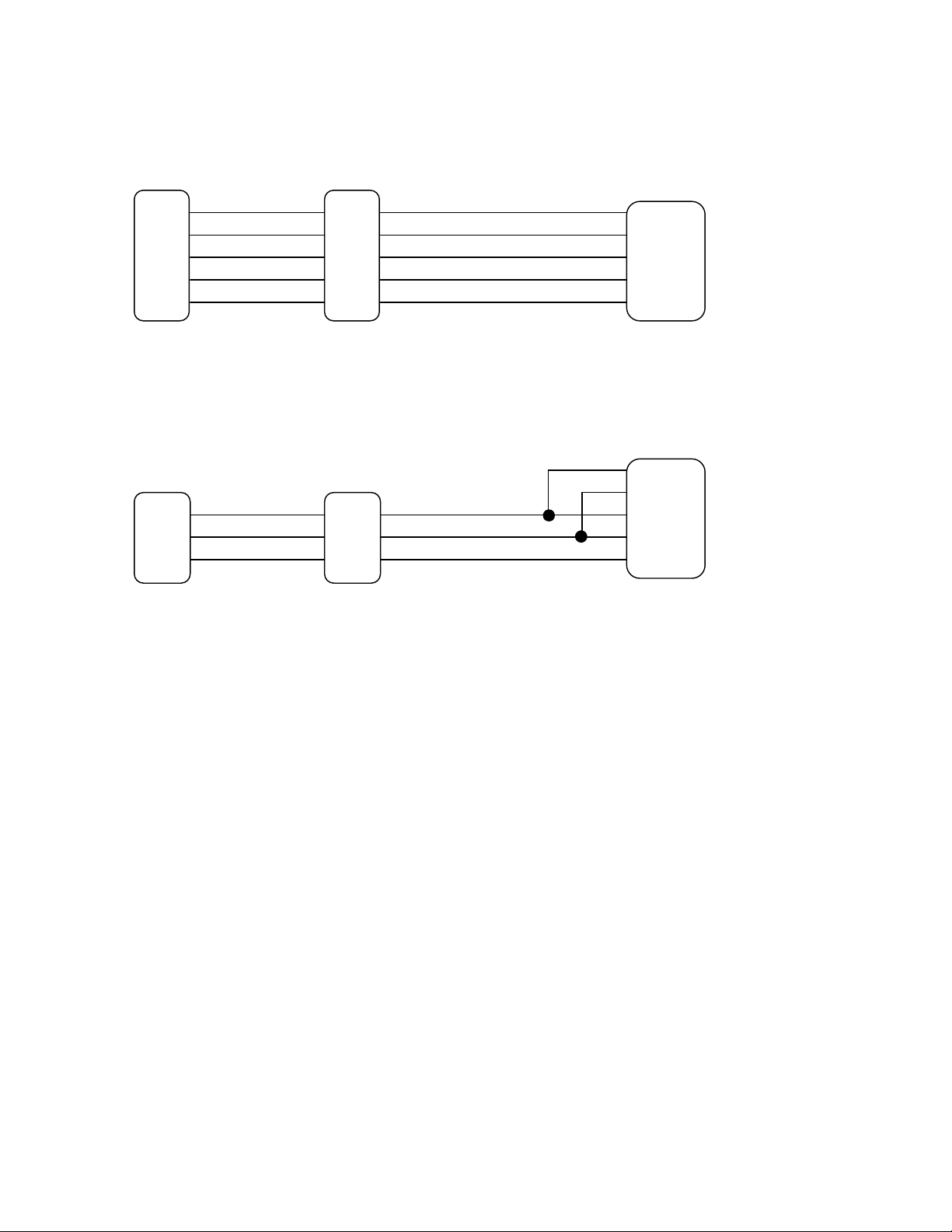
Figure 1: RS232 Wiring
DB-9
2
Rcv
Xmit
Gnd
Rcv
Xmit
Gnd
3
Rcv
Xmit
Gnd
3
Rcv
Xmit
Gnd
DB-25
A-51643 Rev. 6 10/06/03 2
Page 9
Chromalox Instruments and Controls
2 5
Protocol™ Plus DB
-
9 Connector
Master Device
3 7
1 5
Protocol™ Plus Connector
5
Protocol™ Plus DB
-
9 Connector
5
Protocol™ Plus Connector
Master Device
3 7
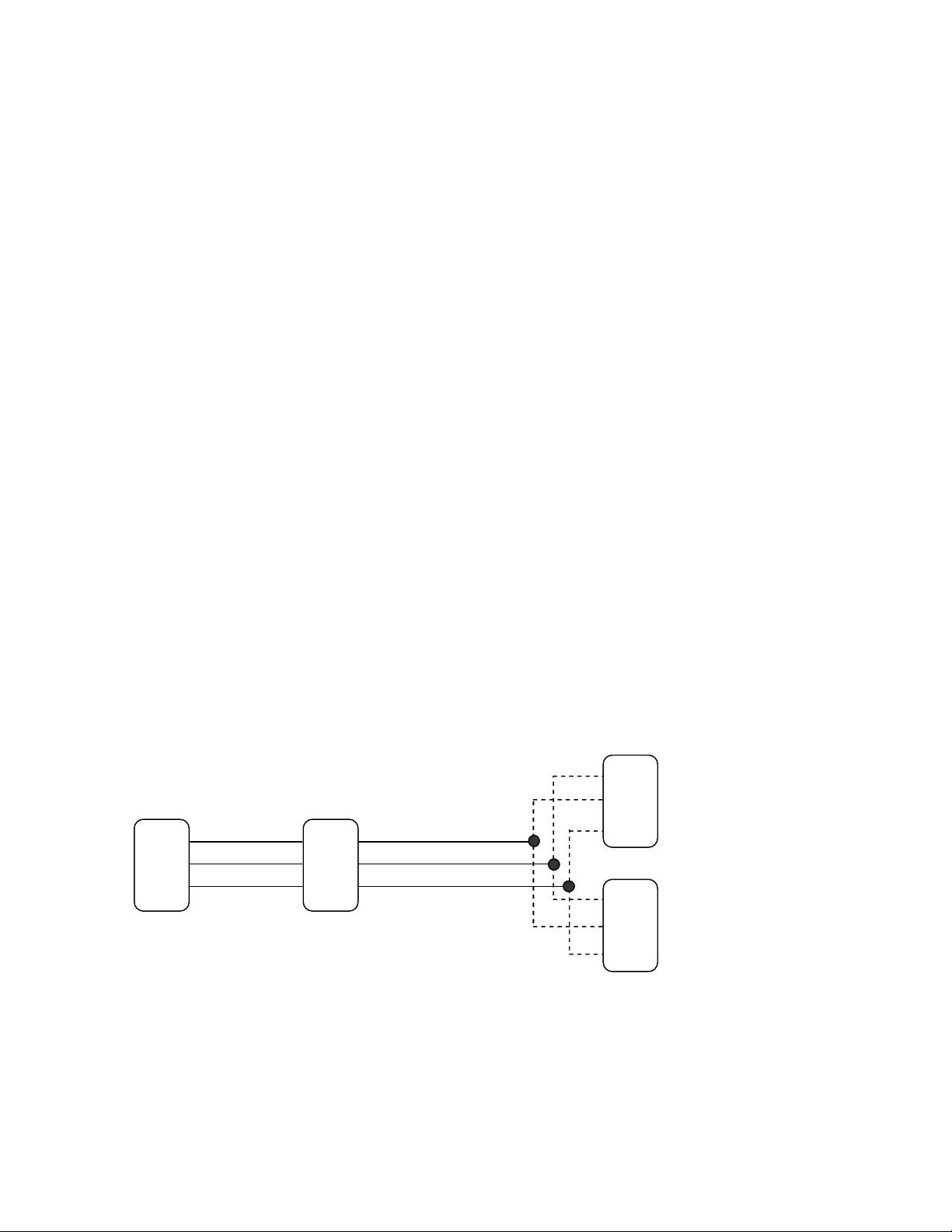
Figure 2: RS422A Wiring (4 wire)
Rcv +
Rcv Xmit +
Xmit - 4
Gnd
T/R +
T/R Gnd
Rcv +
2
3
Rcv -
Xmit +
Xmit - 4
Gnd
7
3
14
2
16
Xmit + (b)
Xmit – (a)
Rcv + (b)
Rcv – (a)
Gnd
DB-25
(Pin #’s based on RS-530
standard; may vary by
device)
Figure 3: RS485 Wiring (2 wire)
14
Xmit + (b)
2
3
4
T/R +
T/R Gnd
3
4
16
Xmit – (a)
Rcv + (b)
Rcv – (a)
Gnd
DB-25
(Pin #’s based on RS-530
standard; may vary by
device)
2.4 Communication Card Installation and Jumper Settings
WARNING
Electronic Components are extremely sensitive to static electricity. Before opening the controller
case, read and follow the precautions below to prevent damage from static electricity.
1. Turn off power to the controller.
2. Touch a bare metal surface on the exterior of the controller.
3. Disconnect the power connection from the controller or unplug from the power source.
Also follow these static electricity precautions:
v Avoid static-causing surfaces while working with electronic components.
v Remove parts from their anti-static bags only when ready for use. Do not lay parts on the outside of
the anti-static bag because only the inside provides protection.
v Hold circuit boards by their edges or any metal mounting hardware. Avoid touching components or
connectors on the circuit boards.
2.4.1 Communication Card (0113-10175) Installation
1. Turn off power to the controller.
2. Remove the back cover of the controller by removing the two screws at the top of the unit.
A-51643 Rev. 6 10/06/03 3
Page 10
Chromalox Instruments and Controls
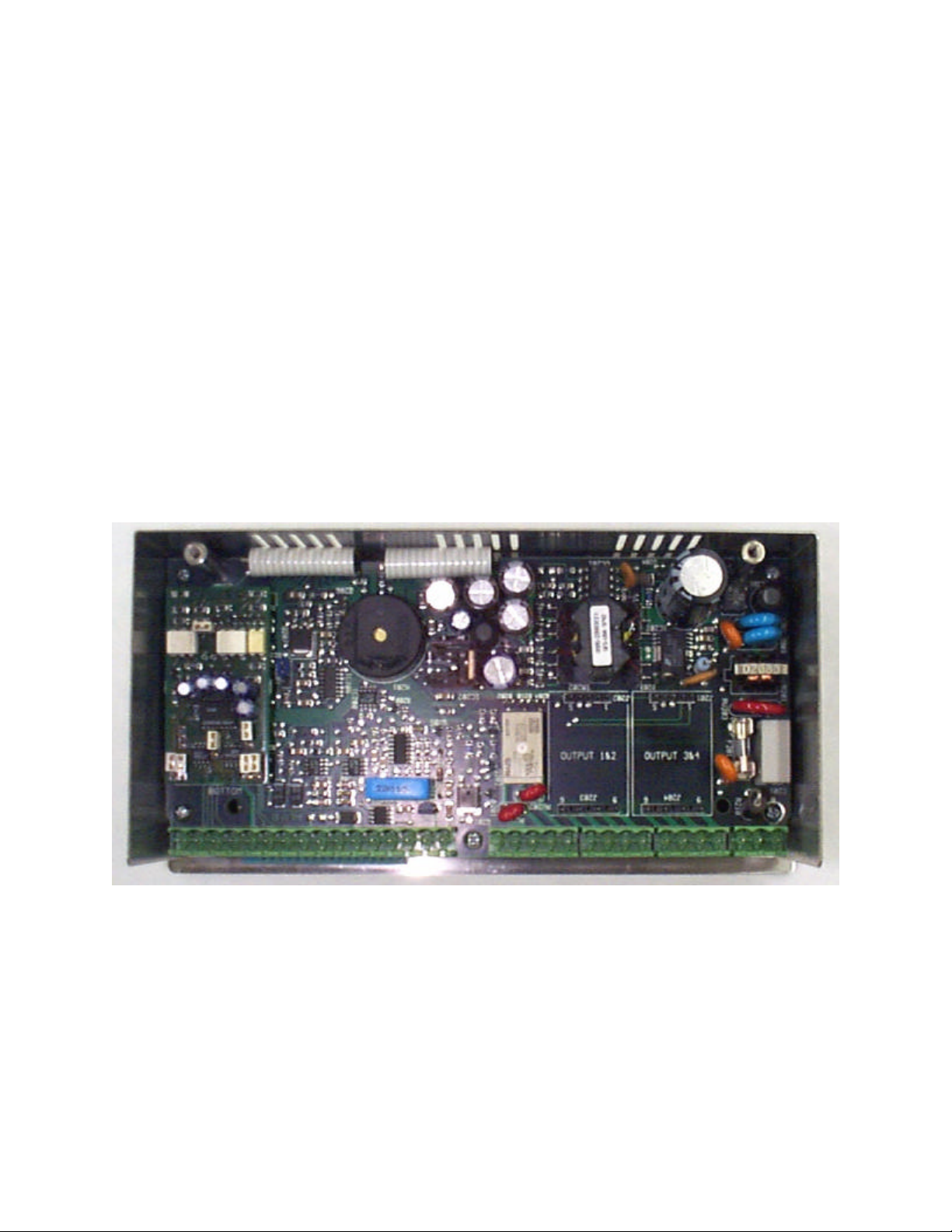
3. Looking into the back of the controller with the connector terminal strips at the bottom, install the
communication card onto the two 5 pin headers on the rear circuit board. Be sure the jumper blocks
on the communication card are positioned toward the bottom of the controller. See Figure 4:
Controller Rear View with Communication Card (Left). Be sure the card is seated firmly onto the
headers.
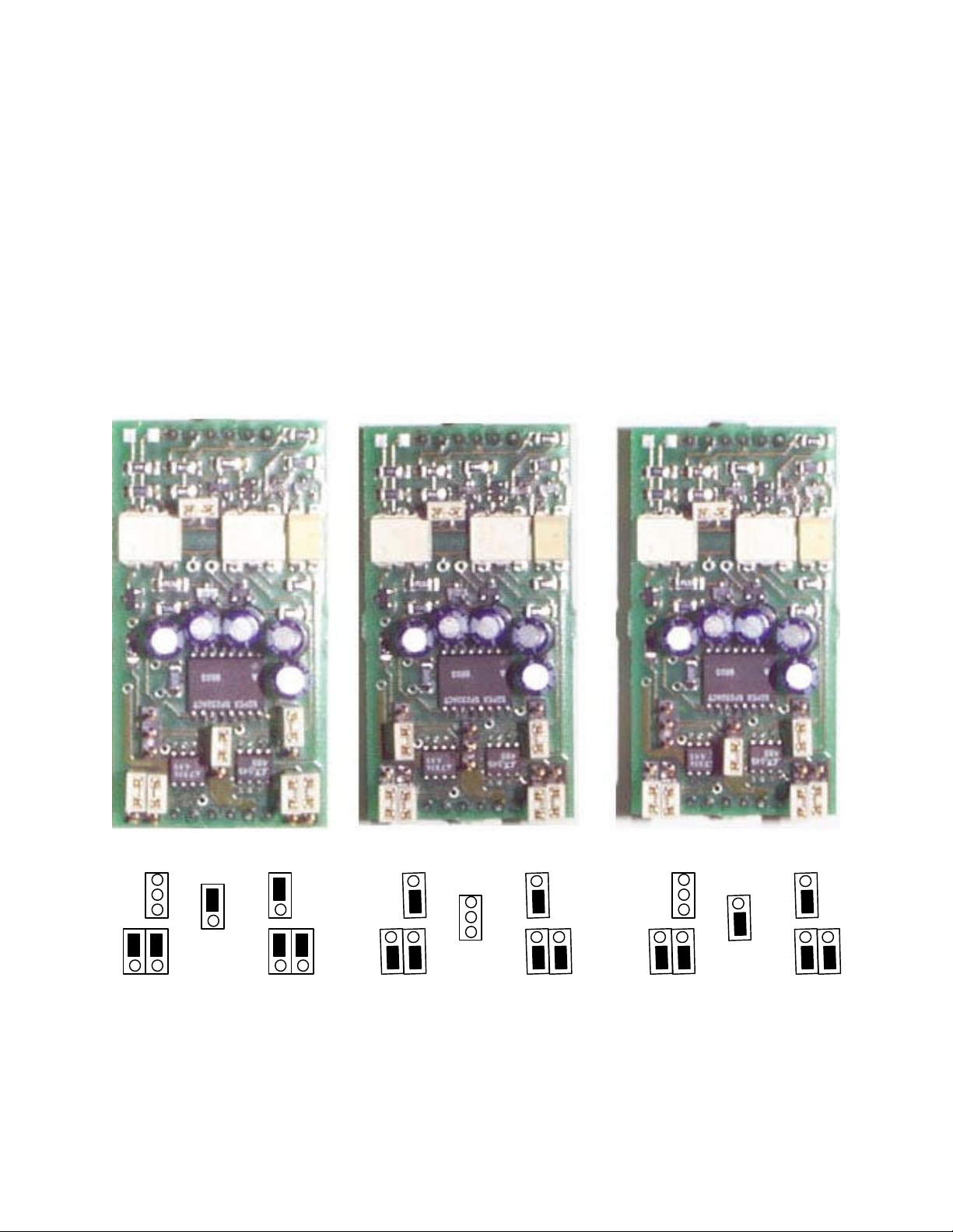
4. Set the jumpers on the communication card for the desired serial communication interface based on
Figure 5: Communication Card (0113-10175) Jumper Settings.
5. Reinstall the back cover.
6. Wire the communication connections on the rear of the unit for the desired serial communication
interface based on Figure 1: RS232 Wiring, Figure 2: RS422A Wiring (4 wire), or Figure 3:
RS485 Wiring (2 wire).
7. Reapply all power connections to the controller.
Figure 4: Controller Rear View with Communication Card (Left)
A-51643 Rev. 6 10/06/03 4
Page 11
Chromalox Instruments and Controls
RS232 Jumper Settings
RS422 Jumper Settings
RS485 Jumper Settings
2.4.2 Communication Card Jumper Settings
1. Turn off power to the controller.
2. Remove the back cover of the controller (if it is not already removed) by removing the two screws at
the top of the unit.
3. Set the jumpers on the communication card for the desired serial communication interface based on
Figure 5: Communication Card (0113-10175) Jumper Settings.
4. Reinstall the back cover.
5. Reapply power to the controller.
Figure 5: Communication Card (0113-10175) Jumper Settings
A-51643 Rev. 6 10/06/03 5
Page 12

Chromalox Instruments and Controls
3 Register and I/O Mapping
3.1 Unmapped and Reserved Registers
Reserved and NA registers will be read as zero with no exception error being generated. Thus, the host
can request data from multiple addresses with gaps between and still receive a valid response. Illegal and
undefined register address blocks will always generate an illegal data address exception.
Reserved and NA registers may be written without generating an exception, however the data is ignored
for these registers and no write takes place. Illegal and undefined register address blocks will always
generate an illegal data address exception.
3.2 Register Quantity Limitations
The number of registers that can be accessed in one query is limited to 50.
3.3 Discrete Input Assignments
The status of the four event inputs can be read as discrete inputs in Modbus format.
Table 3: ProtocolTM Plus Discrete Input Address Map
Data Address Hex Address Description Security
8 -- 65535
0
1
2
3
4 -- 7
$0000 Event Input 1
$0001 Event Input 2
$0002 Event Input 3
$0003 Event Input 4
$0004 -- $0007 Illegal, Reserved for future inputs
$0008 - $FFFF Undefined, available for application assignment
0
0
0
0
0
0
3.4 Discrete Output Assignments
The status of the four relay outputs can be read as discrete outputs in Modbus format. Writes to the
outputs are not supported, that is, the functions “Write Single Output” (06) and “Write Multiple Outputs”
(15) are not implemented.
A-51643 Rev. 6 10/06/03 6
Page 13

Chromalox Instruments and Controls
Table 4: ProtocolTM Plus Discrete Output Address Map
Data Address Hex Address Description Security
8 -- 65535
0
1
2
3
4 -- 7
$0000 Relay Output 1
$0001 Relay Output 2
$0002 Relay Output 3
$0003 Relay Output 4
$0004 -- $0007 Illegal, Reserved for future inputs
$0008 - $FFFF Undefined, available for application assignment
0
0
0
0
0
0
A-51643 Rev. 6 10/06/03 7
Page 14

Chromalox Instruments and Controls
Timer/Ramp/Soak Interval Time
0 = ramp interval of segment, 1 = soak interval of
3.5 Input Register Assignments
Input registers are intended for read only information and functions that cannot or should not be
controlled remotely. Much status information is mapped as holding registers so that operations can be
controlled remotely. Examples are control output commands, ramp/soak status (run, hold, stop), and
ramp/soak program number.
Table 5: ProtocolTM Plus Input Register Address Map
Page[menu]
Data
Address
Hex
Address
Description
Association or
Range
Security
Level Comments
Control Loop Input Registers
0 0 PV Sensor range 0 read as xxxx deg. F
1 1 Active SP Sensor range 0 read as xxxx deg. F
2 2 Active Hi Limit SP Sensor range 0 read as xxxx deg. F
3 3 PV Status -1, 0, 1 0 -1 = underrange, 0 = in range, 1 = overrange
4 4 NA 0 0
5 5 Hi Limit PV Sensor Range 0 read as xxxx deg. F
6 6 Hi Limit PV Status -1, 0, 1 0 -1 = underrange, 0 = in range, 1 = overrange
7 7 Control Output Command 0 - 100.0 0 value has an implied decimal pt. of 1
8 8 Hi Limit Output 0, 1 0 0 = Off, 1 = On
9 9 Max Hi Limit SP Control[Hi-Lim SP] 0 read as xxxx deg. F
10 A NA 0 0
11 B PV Max Sensor Range 0 read as xxxx deg. F
12 C PV Min Sensor Range 0 read as xxxx deg. F
13 D Reserved for factory use
14 E Reserved for factory use
15 F Reserved for factory use
16 -- 127 10 -- 7F Illegal, Reserved standard reg.
Timer/Profile Input Registers
128 80 Segment Number 1-99 0 Current segment number
129 81
130 82 Segment Loops Remaining 0 - 99 0 Number of loops remaining in the ramp/soak program.
131 83 Ramp/Soak Interval Indicator 0, 1 0
132 -- 143 84 -- 8F Illegal, Available to application
Remaining
Global Input Registers
144 90 Terminal Temp (CJC) Ambient Range 0 read as xxx.x deg. F
145 91 N/A 0 0
146 92 Reset Counter 0 - $FFFF 0 Number of processor resets.
147 93 Power Down Counter 0 - $FFFF 0 Number of power down interrupts.
148 94 Alarms Status 0 - $F 0 Bits 0-3 = Alarms 1-4. Bit value: 0 = Off, 1 = On
00:00 - 99:59 0 Time remaining in ramp/soak interval
segment
A-51643 Rev. 6 10/06/03 8
Page 15

Chromalox Instruments and Controls
149 95 Events Status 0 - $F 0 Bits 0-3 = Events 1-4. Bit value: 0 = Off, 1 = On
150 96 Cycle Complete Status 0, 1 0 0 = Off, 1 = On
151 97 Audible Annunciator Status 0, 1 0 0 = Off, 1 = On
152 -- 155 98 -- 9B Reserved, available to application 0 0
156 – 157 9C – 9D Reserved for factory use
158 -- 159 9E – 9F N/A 0 0
A/D Input Registers
160 -- 165 A0 -- A5 Reserved for factory use
166 -- 167 A6 -- A7 Illegal, Reserved standard reg.
168 -- 175 A8 -- AF Illegal, Available to application
Allocated
Blocks
176 -- 255 B0 -- FF Illegal, Reserved standard reg.
256 -- 65535 100 -- FFFF Undefined
A-51643 Rev. 6 10/06/03 9
Page 16
Chromalox Instruments and Controls
3.6 Holding Register Assignments
Holding registers are intended for information and functions that can be read or written. Each holding
register has a corresponding internal memory variable in the slave device. This association is shown in
the address map table.
Table 6: ProtocolTM Plus Holding Register Address Map
Page[menu]
Association or
Data
Address
Hex
Address
Description
Global Holding Registers
0 0 Communications Security Code 0-999 (0) 0 Security code setting for remote interface.
1 1 Temperature Display Units PID[Temp Unit] 1 or 2 (Note 1) 0 = deg. F, 1 = deg. C.
2 2 Reserved for factory use
3 3 Reserved for factory use
4 4 Reserved for factory use
5 5 Keypad Lockout 0 = normal, 1 = locked (0) 2 Disables front panel keypad
6 6 Controller Mode
7 7 Alarm Acknowledge 0 - $FFF F 0 0 = No Action, >0 = Alarm Acknowledge
8 8 Level 1 Password Enable[Password 1] 2 0 – 999 (Write not allowed while in setup mode)
9 9 Level 2 Password Enable[Password 2] 2 0 – 999 (Write not allowed while in setup mode)
10 A Key Press Beep Control[Key Beep] 1 or 2 (Note 1) 0 = off, 1 = on
11 B End of Cycle Beep Control[EOC Beep] 1 or 2 (Note 1) 0 = off, 1 = on
12 C Alarm Beep Control[Alarm Beep] 1 or 2 (Note 1) 0 = off, 1 = on
13 D Setpoint Change Enable Enable[SPChange] 2 0 = no, 1 = yes
14 E Analog output type Enable[Aout] 2 0 = Control (Default), 1 = Process
15 F Reserved, Available to application 0 0
Control Loop Holding Registers
16 10 Manual SP Manual[setpt] 0 read/written as xxxx deg. F.
17 11 Manual High Limit SP Manual[Hi-Lim SP] 0 read/written as xxxx deg. F.
18 12 Manual Event 1-4 Setup $0 - $F ($0) 0 Bits 0-3 = Events 1-4. Bit value: 0 = Off, 1 = On
19 13 NA 0 0
20 14 Proportional Band (Heat) PID[P (H)] 1 or 2 (Note 1) read/written as xxxx deg. F.
21 15 Integral Reset (Heat) PID[I (H) Rep/Min] 1 or 2 (Note 1) value is in repeats/min
22 16 Derivative Rate (Heat) PID[I (H) in sec] 1 or 2 (Note 1) value is in seconds
23 17 Hysteresis Control[Hysteresis] 1 or 2 (Note 1) read/written as xxxx deg. F.
24 18 High Limit Band Control[Hi-Lim Band] 1 or 2 (Note 1) read/written as xxxx deg. F. 4 = Off.
25 19 Cycle Time Control[Cycle Time Sec] 1 or 2 (Note 1) value is in seconds
26 1A Proportional Band (Cool) PID[P(C)] 1 or 2 (Note 1) read/written as xxxx deg. F. (H/C Version 3.1 Only)
27 1B Integral Reset (Cool) PID[I (C) Rep/Min] 1 or 2 (Note 1) value is in repeats/min. (H/C Version 3.1 Only)
28 1C Derivative Rate (Cool) PID[D(C) in Sec] 1 or 2 (Note 1) Value is in Seconds. (H/C Version 3.1 Only)
29 1D Heat Offset PID[Heat Offset] 1 or 2 (Note 1) read/written as xxxx deg. F. (+/- P Band H) H/C Only
30 1E Cool Offset PID[Cool Offset] 1 or 2 (Note 1) read/written as xxxx deg. F. (+/- P Band H) H/C Only
Range (default
value)
Read: 1 – 5
Write: 1 - 4
Security
Level Comments
0 1=Manual, 2=Timer, 3=Profile, 4=Autostart, 5=Setup
A-51643 Rev. 6 10/06/03 10
Page 17

Chromalox Instruments and Controls
31 1F Control Type Control[Ctrl] 1 or 2 (Note 1) 0 = Heat, 1 = Cool, 2 = Heat/Cool. H/C Only
32 – 34 20 – 22 NA 0 0
35 23 Auto Tune Enable PID[Auto Tune] 1 or 2 (Note 1) 0 = Disabled, 1 = Enabled
36 24 Power Up Start Enable Control[PwrUpStrt] 1 or 2 (Note 1) 0 = Disabled, 1 = Enabled
37 25 Power Up Start Mode Control[StrtMode] 1 or 2 (Note 1) 0=Off, 1=Manual, 2=Timer, 3-10=Profile 1-8
38 – 39 26 – 27 NA 0 0
40 28 Power Fail Recovery Control[PwrFRec] 1 or 2 (Note 1) 0=Stop, 1=Restart, 2=Hold, 3=Resume
41 29 Recovery Time Limit Control[PFRTime] 1 or 2 (Note 1) 00h00m to 99h59m
42 – 44 2A – 2C NA 0 0
45 2D SP Low Limit Enable[SPLowerLim] 2 read/written as xxxx deg. F.
46 2E SP Upper Limit Enable[SPUpperLim] 2 read/written as xxxx deg. F.
47 2F High Limit Over Head Enable[HiLimOH] 2 read/written as xxxx deg. F.
48 – 53 30 – 35 NA 0 0
54 36 Process Out Scale Low Control[RetOutLo] 1 or 2 (Note 1) read/written as xxxx deg. F.
55 37 Process Out Scale High Control[RetOutHi] 1 or 2 (Note 1) read/written as xxxx deg. F.
56 – 63 38 – 3F Illegal, Available to application
Timer Holding Registers
64 40 Timer SP Timer[Setpt] 0 read/written as xxxx deg. F.
65 41 Timer High Limit SP Timer[Hi-Lim SP] 0 read/written as xxxx deg. F.
66 42 Timer Event 1-4 Setup $0 - $F ($0) 0 Bits 0-3 = Events 1-4. Bit value: 0 = Off, 1 = On
67 43 Timer Value Timer[Time Set] 0 read/written as xx:xx hrs:min or min:sec
68 44 Timer Guaranteed Soak Band Timer[TmrGuarSoak] 0 read/written as xxxx deg. F. 0 = Off.
69 -- 399 45 -- 18F Illegal, Reserved standard reg.
Control Operation and Profile Holding Registers
400 190 NA 0 0
401 191 Profile Number 0 - 8 0 Current Profile number; 0= none;
402 192 Run/Hold/Stop Control 0 - 2 0 0 = Stop key, 1 or 2 = Run/Hold key
403 193 Time Scale Control[TimeScale] 1 or 2 (Note 1) 0 = mm:ss, 1 = hh:mm
404 194 Segment Advance 0 - $FFFF 0 0=no action; >0 = advance to next segment
Profile 1
405 195 Segment 1 Ramp Time Seg-1 Ramp[Time] 1 or 2 (Note 1) read/written as xx:xx hrs:min or min:sec
406 196 Segment 1 Ramp Event 1-4 Setup Seg-1 Ramp[Event1-4] 1 or 2 (Note 1) Bits 0-3 = Events 1-4. Bit value: 0 = Off, 1 = On
407 197 Segment 1 Soak Temp Seg-1 Soak[Temp] 1 or 2 (Note 1) read/written as xxxx deg. F.
408 198 Segment 1 Soak Time Seg-1 Soak[Time] 1 or 2 (Note 1) read/written as xx:xx hrs:min or min:sec
409 199 Segment 1 Soak Event 1-4 Setup Seg-1 Soak[Event1 -4] 1 or 2 (Note 1) Bits 0-3 = Events 1-4. Bit value: 0 = Off, 1 = On
410 19A Segment 2 Ramp Time Seg-2 Ramp[Time] 1 or 2 (Note 1) read/written as xx:xx hrs:min or min:sec
411 19B Segment 2 Ramp Event 1-4 Setup Seg-2 Ramp[Event1-4] 1 or 2 (Note 1) Bits 0-3 = Events 1-4. Bit value: 0 = Off, 1 = On
412 19C Segment 2 Soak Temp Seg-2 Soak[Temp] 1 or 2 (Note 1) read/written as xxxx deg. F.
413 19D Segment 2 Soak Time Seg-2 Soak[Time] 1 or 2 (Note 1) read/written as xx:xx hrs:min or min:sec
414 19E Segment 2 Soak Event 1-4 Setup Seg-2 Soak[Event1-4] 1 or 2 (Note 1) Bits 0-3 = Events 1-4. Bit value: 0 = Off, 1 = On
415 19F Segment 3 Ramp Time Seg-3 Ramp[Time] 1 or 2 (Note 1) read/written as xx:xx hrs:min or min:sec
416 1A0 Segment 3 Ramp Event 1-4 Setup Seg-3 Ramp[Event1-4] 1 or 2 (Note 1) Bits 0-3 = Events 1-4. Bit value: 0 = Off, 1 = On
417 1A1 Segment 3 Soak Temp Seg-3 Soak[Temp] 1 or 2 (Note 1) read/written as xxxx deg. F.
418 1A2 Segment 3 Soak Time Seg-3 Soak[Time] 1 or 2 (Note 1) read/written as xx:xx hrs:min or min:sec
419 1A3 Segment 3 Soak Event 1-4 Setup Seg-3 Soak[Event1 -4] 1 or 2 (Note 1) Bits 0-3 = Events 1-4. Bit value: 0 = Off, 1 = On
420 1A4 Segment 4 Ramp Time Seg-4 Ramp[Time] 1 or 2 (Note 1) read/written as xx:xx hrs:min or min:sec
A-51643 Rev. 6 10/06/03 11
Page 18

Chromalox Instruments and Controls
421 1A5 Segment 4 Ramp Event 1-4 Setup Seg-4 Ramp[Event1-4] 1 or 2 (Note 1) Bits 0-3 = Events 1-4. Bit value: 0 = Off, 1 = On
422 1A6 Segment 4 Soak Temp Seg-4 Soak[Temp] 1 or 2 (Note 1) read/written as xxxx deg. F.
423 1A7 Segment 4 Soak Time Seg-4 Soak[Time] 1 or 2 (Note 1) read/written as xx:xx hrs:min or min:sec
424 1A8 Segment 4 Soak Event 1-4 Setup Seg-4 Soak[Event1 -4] 1 or 2 (Note 1) Bits 0-3 = Events 1-4. Bit value: 0 = Off, 1 = On
425 1A9 Segment 5 Ramp Time Seg-5 Ramp[Time] 1 or 2 (Note 1) read/written as xx:xx hrs:min or min:sec
426 1AA Segment 5 Ramp Event 1-4 Setup Seg-5 Ramp[Event1-4] 1 or 2 (Note 1) Bits 0-3 = Events 1-4. Bit value: 0 = Off, 1 = On
427 1AB Segment 5 Soak Temp Seg-5 Soak[Temp] 1 or 2 (Note 1) read/written as xxxx deg. F.
428 1AC Segment 5 Soak Time Seg-5 Soak[Time] 1 or 2 (Note 1) read/written as xx:xx hrs:min or min:sec
429 1AD Segment 5 Soak Event 1-4 Setup Seg-5 Soak[Event1-4] 1 or 2 (Note 1) Bits 0-3 = Events 1-4. Bit value: 0 = Off, 1 = On
430 1AE Segment 6 Ramp Time Seg-6 Ramp[Time] 1 or 2 (Note 1) read/written as xx:xx hrs:min or min:sec
431 1AF Segment 6 Ramp Event 1-4 Setup Seg-6 Ramp[Event1-4] 1 or 2 (Note 1) Bits 0-3 = Events 1-4. Bit value: 0 = Off, 1 = On
432 1B0 Segment 6 Soak Temp Seg-6 Soak[Temp] 1 or 2 (Note 1) read/written as xxxx deg. F.
433 1B1 Segment 6 Soak Time Seg-6 Soak[Time] 1 or 2 (Note 1) read/written as xx:xx hrs:min or min:sec
434 1B2 Segment 6 Soak Event 1-4 Setup Seg-6 Soak[Event1-4] 1 or 2 (Note 1) Bits 0-3 = Events 1-4. Bit value: 0 = Off, 1 = On
435 1B3 Segment 7 Ramp Time Seg-7 Ramp[Time] 1 or 2 (Note 1) read/written as xx:xx hrs:min or min:sec
436 1B4 Segment 7 Ramp Event 1-4 Setup Seg-7 Ramp[Event1-4] 1 or 2 (Note 1) Bits 0-3 = Events 1-4. Bit value: 0 = Off, 1 = On
437 1B5 Segment 7 Soak Temp Seg-7 Soak[Temp] 1 or 2 (Note 1) read/written as xxxx deg. F.
438 1B6 Segment 7 Soak Time Seg-7 Soak[Time] 1 or 2 (Note 1) read/written as xx:xx hrs:min or min:sec
439 1B7 Segment 7 Soak Event 1-4 Setup Seg-7 Soak[Event1-4] 1 or 2 (Note 1) Bits 0-3 = Events 1-4. Bit value: 0 = Off, 1 = On
440 1B8 Segment 8 Ramp Time Seg-8 Ramp[Time] 1 or 2 (Note 1) read/written as xx:xx hrs:min or min:sec
441 1B9 Segment 8 Ramp Event 1-4 Setup Seg-8 Ramp[Event1-4] 1 or 2 (Note 1) Bits 0-3 = Events 1-4. Bit value: 0 = Off, 1 = On
442 1BA Segment 8 Soak Temp Seg-8 Soak[Temp] 1 or 2 (Note 1) read/written as xxxx deg. F.
443 1BB Segment 8 Soak Time Seg-8 Soak[Time] 1 or 2 (Note 1) read/written as xx:xx hrs:min or min:sec
444 1BC Segment 8 Soak Event 1-4 Setup Seg-8 Soak[Event1 -4] 1 or 2 (Note 1) Bits 0-3 = Events 1-4. Bit value: 0 = Off, 1 = On
445 1BD High Limit SP [Hi-Lim SP] 1 or 2 (Note 1) read/written as xxxx deg. F.
446 1BE Loop From Segment # [Loop From Seg No] 1 or 2 (Note 1) 0 = None; 1-8 = Loop from segement.
447 1BF Loop to Segment # [Loop To Seg No] 1 or 2 (Note 1) 0 = None; 1-8 = Loop to segement.
448 1C0 Loop # of Times [Loop Number] 1 or 2 (Note 1) 0-99
449 1C1 Link to Profile [Link To Pro] 1 or 2 (Note 1) -1=Stop, 0=Hold, 1-8=Profile 1-8, -2=Standby.
450 1C2 Guaranteed Soak Band [Guar Band] 1 or 2 (Note 1) read/written as xxxx deg. F. 0 = Off.
Profile 2
451 -- 496 1C3 -- 1F0 Profile 2 Holding Registers (same as Profile 1) 1 or 2 (Note 1)
Profile 3
497 -- 542 1F1 -- 21E Profile 3 Holding Registers (same as Profile 1) 1 or 2 (Note 1)
Profile 4
543 -- 588 21F -- 24C Profile 4 Holding Registers (same as Profile 1) 1 or 2 (Note 1)
Profile 5
589 -- 634 24D -- 27A Profile 5 Holding Registers (same as Profile 1) 1 or 2 (Note 1)
Profile 6
635 -- 680 27B -- 2A8 Profile 6 Holding Registers (same as Profile 1) 1 or 2 (Note 1)
Profile 7
681 -- 726 2A9 -- 2D6 Profile 7 Holding Registers (same as Profile 1) 1 or 2 (Note 1)
Profile 8
727 -- 772 2D7 -- 304 Profile 8 Holding Registers (same as Profile 1) 1 or 2 (Note 1)
Auto Start Holding Registers
773 305 Auto Start Enable Auto Start[Enable] 1 or 2 (Note 1) 0 = Disabled, 1 = Enabled
A-51643 Rev. 6 10/06/03 12
Page 19

Chromalox Instruments and Controls
774 306 Sunday Run Mode Auto Start Sun[Mode] 1 or 2 (Note 1) 0=Off, 1=Manual, 2=Timer, 3-10=Profile 1-8
775 307 Sunday Run Time Auto Start Sun[Time] 1 or 2 (Note 1) 00h00m to 23h59m
776 308 Monday Run Mode Auto Start Mon[Mode] 1 or 2 (Note 1) 0=Off, 1=Manual, 2=Timer, 3-10=Profile 1-8
777 309 Monday Run Time Auto Start Mon[Time] 1 or 2 (Note 1) 00h00m to 23h59m
778 30A Tuesday Run Mode Auto Start Tue[Mode] 1 or 2 (Note 1) 0=Off, 1=Manual, 2=Timer, 3-10=Profile 1-8
779 30B Tuesday Run Time Auto Start Tue[Time] 1 or 2 (Note 1) 00h00m to 23h59m
780 30C Wednesday Run Mode Auto Start Wed[Mode] 1 or 2 (Note 1) 0=Off, 1=Manual, 2=Timer, 3-10=Profile 1-8
781 30D Wednesday Run Time Auto Start Wed[Time] 1 or 2 (Note 1) 00h00m to 23h59m
782 30E Thursday Run Mode Auto Start Thu[Mode] 1 or 2 (Note 1) 0=Off, 1=Manual, 2=Timer, 3-10=Profile 1-8
783 30F Thursday Run Time Auto Start Thu[Time] 1 or 2 (Note 1) 00h00m to 23h59m
784 310 Friday Run Mode Auto Start Fri[Mode] 1 or 2 (Note 1) 0=Off, 1=Manual, 2=Timer, 3-10=Profile 1-8
785 311 Friday Run Time Auto Start Fri[Time] 1 or 2 (Note 1) 00h00m to 23h59m
786 312 Saturday Run Mode Auto Start Sat[Mode] 1 or 2 (Note 1) 0=Off, 1=Manual, 2=Timer, 3-10=Profile 1-8
787 313 Saturday Run Time Auto Start Sat[Time] 1 or 2 (Note 1) 00h00m to 23h59m
788 -- 1023 314 -- 3FF Illegal, Available to application
Relay Outputs Holding Registers
Relay Output 1
1024 400 Output 1 Type Relay 1[Relay Type] 1 or 2 (Note 1) 0=Off, 1=Alarm, 2=Cycle, 3=Event
1025 401 Relay 1 Action Relay 1[Relay Action] 1 or 2 (Note 1) 0=NDE, 1=NE, 2=NDEL, 3=NEL
1026 402 Alarm 1 Type Relay 1[Alarm Type] 1 or 2 (Note 1) 0 = High, 1 = Low, 2 = +Dev, 3 = -Dev, 4 = +/-Dev
1027 403 Alarm 1 Setpoint Relay 1[AlmHi/LoSP] 1 or 2 (Note 1) read/written as xxxx deg. F.
1028 404 Alarm 1 Deviation Setpoint Relay 1[AlmDevBand] 1 or 2 (Note 1) read/written as xxxx deg. F.
1029 405 Alarm 1 Inhibit Relay 1[AlmInhibit] 1 or 2 (Note 1) 0=Disabled, 1=Enabled
1030 406 Event 1 Type Relay 1[Event Type] 1 or 2 (Note 1) 0=Time, 1=Temp
1031 407 Event 1 Setpoint Relay 1[Event SP] 1 or 2 (Note 1) read/written as xxxx deg. F.
Relay Output 2
1032 -- 1039 408 -- 40F Output 2 Holding Registers (same as Output 1) 1 or 2 (Note 1)
Relay Output 3
1040 -- 1047 410 -- 417 Output 3 Holding Registers (same as Output 1) 1 or 2 (Note 1)
Relay Output 4
1048 -- 1055 418 -- 41F Output 4 Holding Registers (same as Output 1) 1 or 2 (Note 1)
Test Mode Holding Registers
1056 -- 1062 420 -- 426 Reserved for factory use
1063 -- 1135 427 -- 46F Illegal, Available to application
Communication Holding Registers
1136 470 Controller Address Communication[Unit Addr] 1 or 2 (Note 1) 1-247
1137 471 Communications Mode Communication[Enable] 1 or 2 (Note 1) 0=Disabled, 1=Enabled
1138 472 Baud Rate Communication[BaudRate] 1 or 2 (Note 1) 0=2400, 1=4800, 2=9600, 3=19.2K, 4=38.4K
1139 473 Parity Communication[Parity] 1 or 2 (Note 1) 0=None, 1=Odd, 2=Even
1140 474 Reserved, Available to application 0 0
Real Time Clock Holding Registers
1141 475 Week Day Clock[Day] 1 or 2 (Note 1) 1=Sunday, 2=Monday, . . . 7=Saturday
1142 476 Time Clock[hh:mm] 1 or 2 (Note 1) 00h00m to 23h59m
1143 477 Enter Clock[UP to Reset CLK] 1 or 2 (Note 1) 0 = No action, >0 = Set Clock
1144 -- 1151 478 -- 47F Illegal, Reserved for standard reg.
Calibration Holding Registers
A-51643 Rev. 6 10/06/03 13
Page 20

Chromalox Instruments and Controls
1152 -- 1159 480 -- 487 Reserved for factory use
1160 -- 1183 488 -- 49F Illegal, Available to application
1184 -- 1188 4A0 -- 4A4 Reserved for factory use
1189 -- 1199 4A5 -- 4AF Illegal, Available to application
1200 -- 1279 4B0 -- 4FF Illegal, Reserved for standard reg. Reserved for future standard assignments.
Page Enable Holding Registers
1280 500 Program Page 1-8 Enable[Profile 1-8] 2 1 = Yes (security level 1); 0 = No (security level 2)
1281 501 Auto Start Page Enable[Auto Start] 2 1 = Yes (security level 1); 0 = No (security level 2)
1282 502 PID Parameters Page Enable[PID] 2 1 = Yes (security level 1); 0 = No (security level 2)
1283 503 Control Page Enable[Control] 2 1 = Yes (security level 1); 0 = No (security level 2)
1284 504 Communications Page Enable[Communication] 2 1 = Yes (security level 1); 0 = No (security level 2)
1285 505 Real Time Clock Page Enable[Clock] 2 1 = Yes (security level 1); 0 = No (security level 2)
1286 506 Relay Output Page 1-4 Enable[Relay 1-4] 2 1 = Yes (security level 1); 0 = No (security level 2)
1287 507 Test Page Enable[Test] 2 1 = Yes (security level 1); 0 = No (security level 2)
1288 508 Zone Calibration Enable[Zone Cal] 2 1 = Yes (security level 1); 0 = No (security level 2)
1289 509 Sensor Calibration Enable[Sensor Cal] 2 1 = Yes (security level 1); 0 = No (security level 2)
Allocated Blocks
1290 -- 65535 50A -- FFFF Undefined Available for application assignment.
Dependent on enable page setting
NOTES
1
A-51643 Rev. 6 10/06/03 14
Page 21

Chromalox Instruments and Controls
4 Application Operations
This section defines application operations in ProtocolTM Plus controller and how they are achieved
through Modbus.
4.1 Security Level and Discrete Inputs, Discrete Outputs, and Register Access
Access to discrete I/O and registers addresses are guarded via a security level. The communications
security code holding register ($0000) contains the current security setting for accessing data in the
controller through the communications port. Each I/O or register address has an associated preset security
level that controls access. If the current communication security code does not match the register’s
security level, access is denied. An illegal data address exception is generated and data is not changed.
For multiple reads and writes, if any address is inaccessible, an exception response occurs and data is not
affected in the slave.
The communications security operation mirrors the security operation for adjusting parameters through
the front panel keypad. Security levels for each I/O and register address are shown in the I/O and register
mapping tables. The access passwords for security levels 1 and 2 are set via the security level holding
registers ($0008, $0009). The communications security code is set to 0 whenever the controller is
powered up or reset. The access password registers ($0008, $0009) cannot be written to while the
controller is in setup mode to protect adjustments in progress via the front panel keypad.
Table 7: Communication Security Levels
Security Level Description Access Code
0 Global Access Any
1 User Access Level 1 Password Level 1 Menu
2 User Access Level 2 Password Level 2 Menu
3 Factory Only Access ---
4.2 Multiple Register Write Limitations
The Modbus Protocol requires all addresses and all data in a multiple write to be valid for any write to
occur. If an exception response occurs none of the registers are modified. Because all addresses and data
must be verified before the data is actually written, a limitation exists for multiple writes to registers
whose values are interdependent. The verification of data may fail because data to be written to one
register is invalid until data for another register is actually written. In these cases, successive single
register writes must be performed.
A-51643 Rev. 6 10/06/03 15
Page 22

Chromalox Instruments and Controls
An example is the Manual Setpoint and Manual High Limit Setpoint holding registers. If the registers are
currently set to 500 °F and 509 °F respectively, then a multiple write of 300 °F and 350 °F respectively
will fail. During data verification, the high limit value of 350 °F is invalid because the setpoint is set to
500 °F. A single write of 300 °F to Manual Setpoint followed by a single write of 350 °F to Manual High
Limit Setpoint will work.
4.3 Control Operation and Run/Hold/Stop Functions
The 4 control states of the controller (Manual, Timer, Profile, and Autostart) can be set via the Controller
Mode holding register ($0006). The controller mode cannot be changed unless the controller is stopped.
Before changing modes, the STOP value must be written to the Run/Hold/Stop holding register ($0192),
then the desired mode value can be written to the Controller Mode holding register. When reading the
Controller Mode holding register ($0006), a fifth mode (Setup) can be detected. The user cannot place
the controller into setup mode via Modbus because the setup mode applies only to adjusting parameters
via the front panel keypad.
When the controller is in Manual, Timer, or Profile control mode, the Run/Hold/Stop register ($0192) is
used to Run, Hold, or Stop the controller. A value of 0 simulates the STOP key; a value of 1 or 2
simulates the RUN/HOLD key. When in Profile control mode, the Profile Number ($0191) and the
Segment Advance ($0194) holding registers control which profile and segment are being executed. The
Profile Number holding register can only be written when the controller is stopped. A value of 0 sets the
desired profile to none. Writing any non-zero value to the Segment Advance register simulates pressing
the Select/Up Arrow combination while running a profile to advance to the next profile segment.
The Profile Number holding register, along with the Profile Input Registers $0080-$0083 can be read to
monitor the status of the controller. The Segment Number input register ($0080) provides the current
segment number. Input register $0081 provides the time remaining in the current interval and input
register $0082 the number of segment loops remaining. The Ramp/Soak Interval Indicator ($0083) input
register indicates whether the current interval is a ramp or soak interval (0=ramp, 1=soak).
4.4 Controller Mode and Data Access
Most holding registers can only be written to if the controller is stopped. The exceptions are listed below.
All registers can be read in any mode as long as the communications security code is set to the proper
level. An illegal data address response is generated if the controller is not in the correct state to access a
register. The following registers can be written while the controller is running.
A-51643 Rev. 6 10/06/03 16
Page 23

Chromalox Instruments and Controls
REGISTER ADDRESS REGISTER DESCRIPTION
$0000 COMMUNICATIONS ACCESS CODE
$0005 KEYPAD LOCKOUT
$0007 ALARM ACKNOWLEDGE
$0008 LEVEL 1 PASSWORD (write not allowed while in setup mode)
$0009 LEVEL 2 PASSWORD (write not allowed while in setup mode)
$0010 MANUAL SETPOINT
$0040 TIMER SETPOINT
$0192 RUN/HOLD/STOP
$0194 SEGMENT ADVANCE
4.5 Monitoring and Acknowledgement of Alarms, Events, and Cycle Complete, Discrete
Inputs, and Discrete Outputs
Two input registers allow monitoring of the alarm ($0094) and event ($0095) functions associated with
relay outputs 1-4. The corresponding input register represents a binary pattern that indicates the state of
each function. Bits 0-3 of the holding register value represent item 1-4 respectively. A bit value of 0
indicates off, while a bit value of 1 indicates on. Example: A read of holding register $0098 returns a
value of $0006. This would indicate that alarms 2 and 3 are active.
The cycle complete status is monitored by reading input register $0096. A value of 0 indicates the cycle
is active, while a value of 1 indicates the cycle is complete.
Reading the discrete input addresses-$0000 - $00003 monitors the hardware states of the external inputs
Event 1-4. For details on the return values see 5.2.2 [02] Read Input Discretes. Since these inputs are
active low switch inputs, a returned value of 1 (or on) means the input is active (electrically pulled low).
Reading the discrete output addresses-$0000 - $00003 monit ors the hardware states of relays 1-4. For
details on the return values see 5.2.1 [01] Read Outputs.
The audible annunciator can be monitored via input register $0097. A value of 0 indicates the audible
annunciator is off, while a value of 1 indicates on. Acknowledgement of alarms and cycle complete
audible annunciation is handled through the alarm acknowledge holding register ($0007). Writing any
non-zero value to this register will acknowledge the alarm. This register emulates the pressing of the
Page/Reset key during an audible alarm condition.
A-51643 Rev. 6 10/06/03 17
Page 24

Chromalox Instruments and Controls
4.6 Event Setup Values
For Manual, Timer, and Profile events setup, the corresponding holding register represents a binary
pattern that determines each event output state. Bits 0-3 of the holding register value represent Event
outputs 1-4 respectively. A bit value of 0 sets the event output to be off, while a bit value of 1 sets the
output to be on.
4.7 Keypad Lockout
The front panel keypad can be disabled (locked out) by writing the value 1 to the Keypad Lockout
holding register ($0005). A write of 0 will unlock the keypad. The keypad lockout register is always set
to 0 during a power-up or reset of the controller to ensure that the keypad can never be permanently
locked out.
4.8 Temperature Values
Temperature values read from input and holding registers and written to holding registers are always in °F
and assume no decimal place. An exception is the ambient temperature input register ($0090) which
assumes 1 decimal place. A value read or written as 750 would represent 75.0 °F.
4.9 Time Values
Time values are read and written in a format that adheres to the to Modbus standard of two bytes per data
item. The high byte is a hex number representing hours or minutes while the low byte is a hex number
representing minutes or seconds. The units of the two bytes (hhmm or mmss) are dependent of the format
of the specific register being accessed. Example: 12h00m ⇒ $0C00; 36m42s ⇒ $242A.
4.10 High Limit Setpoint and Band Registers
The Despatch Protocol Plus has several special cases involving the adjustment and display of high limit
parameters. Since only values can be returned via Modbus (no special strings), the read/write of these
parameters has been implemented in the simplest manner that still allows for complete functionality.
All high limit setpoint and band registers read and write directly to the parameter associated with the
register address—regardless of whether that value is active due to the setting of another high limit register
(as in the high limit band holding register $0018). To determine the high limit setpoint currently being
used for control, read the Active High Limit Setpoint register $0002.
4.11 Broadcasting with Guaranteed Delivery
Broadcast messages are processed by all slaves and do not generate a response. In order to verify the
delivery, acceptance, and processing of broadcast messages the following procedure can be used.
A-51643 Rev. 6 10/06/03 18
Page 25

Chromalox Instruments and Controls
1. Send an individual function code 08, sub-function 10 queries (clear communication counters) to each
slave on the network.
2. Perform desired broadcast functions.
3. Send an individual function code 08, sub-function 14 queries (return slave message count) to each
slave on the network.
4. If the number of processed messages in each slave matches the number of broadcasts sent then the
broadcast messages were sent reliably.
4.12 Communication Parameter Adjustments
If the communication parameters (slave address, mode, baud rate, or parity) are changed through the front
panel or through the Modbus link, the controller need not be reset. The new parameters (in the controller)
will become effective on the next query/response cycle. However, in some cases, the first query after
changing the settings may not generate a response as this query is used to reset the communication setup.
The user is responsible for setting the master device to the proper settings.
Setting the communications mode to “disabled” will immediately disable communications.
Communications can only be re-enabled through the front panel keypad. Use the force listen mode
command (5.3.1.4 [08 04] Force Listen Mode Only) to temporarily disable communications.
A-51643 Rev. 6 10/06/03 19
Page 26

Chromalox Instruments and Controls
slave and successfully processed.
5 Function Set Details
This section details the Modbus functions supported in the ProtocolTM Plus controller.
5.1 Function Set Overview
Table 8 ProtocolTM Plus Function and Exception Code Set
Function Code Function Name
01 Read Outputs
02 Read Input Discretes
03 Read Holding Register (Read Multiple Registers)
04 Read Input Registers
06 Write Single Register
08 Diagnostics
16 Write Multiple Registers
17 Report Slave ID
Table 9 ProtocolTM Plus Diagnostic (Function Code 08) Sub-function Set
Sub-function Code Sub-function Name Comments
00 Return Query Data Loop Back
01 Restart Communications Options Reset the slave. Cancels Listen Only
Mode.
02 Return Diagnostic Register Contents of slave’s 16-bit diagnostic
register.
04 Force Listen Only Mode Reset by Restart Communications
Option
10 Clear Counters and Diagnostic Register Also cleared at power up. Clears only
the counters
12 Return Bus Communication Error Count Slave CRC errors only.
13 Return Bus Exception Error Count Slave Exception Response count.
14 Return Slave Message Count Number of messages addressed to the
Includes broadcast messages.
A-51643 Rev. 6 10/06/03 20
Page 27

Chromalox Instruments and Controls
15 Return Slave No Response Count Number of messages addressed to the
18 Return Bus Character Overrun Count Number of overrun and framing errors.
Table 10 ProtocolTM Plus Exception Code Set
Exception Code Description Comments
01 Illegal Function The function code received is not valid or
02 Illegal Data Address The data address received is invalid or is
03 Illegal Data Value The data value received is invalid.
slave for which no response was
returned.
is not supported.
not accessible due to security setting.
5.2 Register and I/O Function Set Description for ProtocolTM Plus
5.2.1 [01] Read Outputs
Class 1 command. Reads the On/Off status of discrete outputs in the slave. Broadcast is not supported.
Query
The query message specifies the starting output and quantity of outputs to be read. Outputs are addressed
starting at 0.
Example: Query to read outputs 20 . . . 56 from slave address 17.
Field Name Data
Slave address $11
Function $01
Starting address hi $00
Starting address lo $13
Number of outputs hi $00
Number of outputs lo $25
CRC $----
A-51643 Rev. 6 10/06/03 21
Page 28

Chromalox Instruments and Controls
Response
The output status in the response is packed as one output per bit of the data field. Status is indicated as 0
= Off, 1 = On. The LSB of the first data byte contains the output addressed in the query. The other
outputs follow toward the high order end of this byte, and from low order to high order in subsequent
bytes. If the returned output quantity is not a multiple of eight, the remaining bits in the final data byte
will be padded with zero (toward the high order end). The Byte Count field specifics the quantity of
complete bytes of data.
Example response:
Field Name Data
Slave address $11
Function $01
Byte count $05
Data (outputs 27 . . . 20) $CD
Data (outputs 35 . . . 28) $A0
Data (outputs 43 . . . 36) $36
Data (outputs 51 . . . 44) $FB
Data (outputs 56 . . . 52) $05
CRC $----
5.2.2 [02] Read Input Discretes
Class 1 command. Reads the On/Off status of discrete inputs in the slave. Broadcast is not supported.
Query
The query message specifies the starting input and quantity of inputs to be read. Inputs are addressed
starting at 0.
Example: Request to read inputs 1 . . . 7 from slave address 8.
Field Name Data
Slave address $08
Function $02
Starting address hi $00
Starting address lo $00
A-51643 Rev. 6 10/06/03 22
Page 29

Chromalox Instruments and Controls
Number of outputs hi $00
Number of outputs lo $07
CRC $----
Response
The input status in the response message is packed as one input per bit of the data field. Status is
indicated as 0 = Off, 1 = On. The LSB of the first data byte contains the input addressed in the query.
The other inputs follow toward the high order end of this byte, and from low order to high order in
subsequent bytes. If the returned input quantity is not a multiple of eight, the remaining bits in the final
data byte will be padded with zero (toward the high order end). The Byte Count field specifics the
quantity of complete bytes of data.
Example response:
Field Name Data
Slave address $08
Function $02
Byte count $01
Data (inputs 7 . . . 1) $74
CRC $----
5.2.3 [03] Read Holding Registers (Read Multiple Registers)
Class 0 command. Reads the contents of holding registers in the slave. Broadcast is not supported.
Query
The query message specifies the starting register and quantity of registers to be read. Registers are
addressed starting at 0.
Example: Request to read registers 108 . . . 110 from slave address 1.
Field Name Data
Slave address $01
Function $03
Starting address hi $00
Starting address lo $6B
A-51643 Rev. 6 10/06/03 23
Page 30

Chromalox Instruments and Controls
Number of registers hi $00
Number of registers lo $03
CRC $----
Response
The register data in the response message are packed as two bytes per register (one word). For each
register, the first byte contains the high order bits and the second contains the low order bits.
Example response:
Field Name Data
Slave address $01
Function $03
Byte count $06
Data (register 108 hi) $00
Data (register 108 lo) $1E
Data (register 109 hi) $10
Data (register 109 lo) $26
Data (register 110 hi) $02
Data (register 110 lo) $AC
CRC $----
5.2.4 [04] Read Input Registers
Class 1 command. Read the contents of input registers in the slave. Broadcast is not supported.
Query
The query message specifies the starting register and quantity of registers to be read. Registers are
addressed starting at 0.
Example: Request to read input register 10 from slave device 17.
Field Name Data
Slave address $11
Function $04
Starting address hi $00
A-51643 Rev. 6 10/06/03 24
Page 31

Chromalox Instruments and Controls
Starting address lo $09
Number of registers hi $00
Number of registers lo $01
CRC $----
Response
The register data in the response are packed as two bytes per register (one word). For each register, the
first byte contains the high order bits and the second contains the low order bits.
Example response:
Field Name Data
Slave address $11
Function $04
Byte count $02
Data (register 10 hi) $00
Data (register 10 lo) $23
CRC $----
5.2.5 [06] Write Single Register
Class 1 command. Writes a value into a single holding register. When broadcast, the value is written to
the same register reference in all slaves on the network. Use of broadcast with this command should be
used with caution as the register addressed may differ in function on each slave device in the network.
Note: The written value will remain valid until the controller’s next write to the register through its
keypad or internal logic.
Query
The query message specifies the register reference to be written. Registers are addressed starting at zero.
The requested value is specified in the query data field in two bytes (one word). The first byte represents
the high order bits and the second byte represents the low order bits.
Example: Request to preset register 2 to the value 3 in slave device 14.
A-51643 Rev. 6 10/06/03 25
Page 32

Chromalox Instruments and Controls
Field Name Data
Slave address $0E
Function $06
Register address hi $00
Register address lo $01
Data hi $00
Data lo $03
CRC $----
Response
The normal response is an echo of the query, returned after the register has been written.
Example response:
Field Name Data
Slave address $0E
Function $06
Register address hi $00
Register address lo $01
Data hi $00
Data lo $03
CRC $----
5.2.6 [16] Write Multiple Registers
Class 0 command. Write values into a sequence of holding registers. When broadcast, the values are
written to the same register references in all slaves on the network. Use of broadcast with this command
should be used with caution as the registers addressed may differ in function on each slave device in the
network.
Note: The written values will remain valid until the controller’s next write to the register through its
keypad or internal logic.
Query
The query message specifies the register references to be written. Registers are addressed starting at zero.
The number of registers to be written are transmitted in two bytes (one word) with the first byte being the
A-51643 Rev. 6 10/06/03 26
Page 33

Chromalox Instruments and Controls
high order bits and the second byte the low order bits. Next, the actual number of data bytes is
transmitted (one byte). The requested values are specified in the query data field in two bytes (one word)
per register. The first byte represents the high order bits and the second byte represents the low order bits
of the register value.
Example: Request to preset two registers starting at register 5 to the values of 10 and 258 respectively in
slave device 14.
Field Name Data
Slave address $0E
Function $10
Starting register address hi $00
Starting register address lo $04
Number of registers hi $00
Number of registers lo $02
Byte count $04
Data hi (register 5) $00
Data lo (register 5) $0A
Data hi (register 6) $01
Data lo (register 6) $02
CRC $----
Response
The normal response returns the slave address, function code, starting address, and quantity of registers
written.
Example response:
Field Name Data
Slave address $0E
Function $10
Starting register address hi $00
Starting register address lo $04
Number of registers hi $00
Number of registers lo $02
CRC $----
A-51643 Rev. 6 10/06/03 27
Page 34

Chromalox Instruments and Controls
5.3 Diagnostics and Support Description for ProtocolTM Plus
All of the diagnostic and support functions are unclassified commands that tend to be application
dependent. The Modbus diagnostic function provides a series of tests and information exchange for
checking the integrity of the controller, the communication link, and the status of the controller.
Broadcast is not supported.
5.3.1 [08] Diagnostics
The function uses a two-byte sub-function code field in the query to define the type of test to be
performed. Most of the diagnostic queries use a two-byte data field to send diagnostic data or control
information to the slave. In sub-functions where the data is not required, $0000 is transmitted as data and
is ignored by the slave.
The slave echoes both the function code and sub-function code in a normal response as well as returning
any requested data. The diagnostic query form is shown below. The response is sub-function dependent
and may be application dependent. In cases where no return data is required and the data field was
included in the query, the query data field is echoed in the slave response.
Diagnostic Query Form
Field Name Data
Slave address $XX
Function $08
Sub-function hi $XX
Sub-function lo $XX
Data hi $XX
Data lo $XX
CRC $----
5.3.1.1 [08 00] Return Query Data
The data passed in the query data field is to be returned (looped back) in the response. The entire
response message should be identical to the query.
Example: Return Query Data $AA55 from slave device 2.
A-51643 Rev. 6 10/06/03 28
Page 35

Chromalox Instruments and Controls
Query Response
Field Name Data Field Name Data
Slave address $02 Slave address $02
Function $08 Function $08
Sub-function hi $00 Sub-function hi $00
Sub-function lo $00 Sub-function lo $00
Data hi $AA Data hi $AA
Data lo $55 Data lo $55
CRC $---- CRC $----
5.3.1.2 [08 01] Restart Communications Option
The slave is reset, its communication port initialized and restarted, and all of its communications event
counters cleared. If the slave is currently in Listen Only mode, no response is returned. This function is
the only one that brings the port out of Listen Only mode. If the port is not currently in Listen Only
mode, a normal response is returned. This occurs before the reset is executed. When the slave receives
the query, it attempts a restart and executes its power-up confidence tests. Successful completion of the
tests will bring the port online.
Example: Restart Communications on slave device 2.
Query Response
Field Name Data Field Name Data
Slave address $02 Slave address $02
Function $08 Function $08
Sub-function hi $00 Sub-function hi $00
Sub-function lo $01 Sub-function lo $01
Data hi $00 Data hi $00
Data lo $00 Data lo $00
CRC $---- CRC $----
5.3.1.3 [08 02] Return Diagnostic Register
The contents of the slave’s 16 bit diagnostic register are returned in the response. The assignment of
diagnostic register bits in ProtocolTM Plus controllers is shown below. In the register, bit 15 is the highorder bit. The description is TRUE when the corresponding bit is set to logic 1.
A-51643 Rev. 6 10/06/03 29
Page 36

Chromalox Instruments and Controls
Table 11: ProtocolTM Plus Diagnostic Register Bit Assignment
Bit # Description
0 NA
1 NA
2 EEPROM Data Error
3 NA
4 NA
5 NA
6 NA
7 A/D
8 Not Used – Loop Error
9 Not Used – Tune Error
10 Not Used -- Available for Application Specific Support
11 Not Used -- Available for Application Specific Support
12 Not Used -- Available for Application Specific Support
13 Not Used -- Available for Application Specific Support
14 Not Used -- Available for Application Specific Support
15 Not Used -- Available for Application Specific Support
Example: Return the diagnostic register from slave device 2 (with an EEPROM error).
Query Response
Field Name Data Field Name Data
Slave address $02 Slave address $02
Function $08 Function $08
Sub-function hi $00 Sub-function hi $00
Sub-function lo $02 Sub-function lo $02
Data hi $00 Data hi $00
Data lo $00 Data lo $04
CRC $---- CRC $----
5.3.1.4 [08 04] Force Listen Mode Only
Forces the slave into Listen Only Mode. This isolates it from the other devices on the network, allowing
them to continue communicating without interruption form the addressed slave. No response is returned.
When the slave enters this mode, all active communications are turned off. All messages broadcast or
A-51643 Rev. 6 10/06/03 30
Page 37

Chromalox Instruments and Controls
addressed to the slave are monitored, but no action is taken and no responses sent. The Restart
Communications Option function is the only command that will bring the slave out of Listen Only Mode.
Example: Force slave device 23 into Listen Only Mode.
Query No Response
Field Name Data
Slave address $17
Function $08
Sub-function hi $00
Sub-function lo $04
Data hi $00
Data lo $00
CRC $----
5.3.1.5 [08 10] Clear Communication Counters
Clears all communication diagnostic counters. Counters are also cleared upon a controller reset.
Example: Clear communication counters in slave device 23.
Query Response
Field Name Data Field Name Data
Slave address $17 Slave address $17
Function $08 Function $08
Sub-function hi $00 Sub-function hi $00
Sub-function lo $0A Sub-function lo $0A
Data hi $00 Data hi $00
Data lo $00 Data lo $00
CRC $---- CRC $----
5.3.1.6 [08 12] Return Bus Communication Error Count
The response data field returns the quantity of CRC errors encountered by the slave since its last reset or
clear counters command.
Example: Return bus communication error count in slave device 9.
A-51643 Rev. 6 10/06/03 31
Page 38

Chromalox Instruments and Controls
Query Response
Field Name Data Field Name Data
Slave address $09 Slave address $09
Function $08 Function $08
Sub-function hi $00 Sub-function hi $00
Sub-function lo $0C Sub-function lo $0C
Data hi $00 Data hi $00
Data lo $00 Data lo $07
CRC $---- CRC $----
5.3.1.7 [08 13] Return Bus Exception Error Count
The response data field returns the quantity of Modbus exception responses returned by the slave since its
last reset or clear counters command. For a description of exception responses see 5.4 Exception
Response Description.
Example: Return bus exception count in slave device 3.
Query Response
Field Name Data Field Name Data
Slave address $03 Slave address $03
Function $08 Function $08
Sub-function hi $00 Sub-function hi $00
Sub-function lo $0D Sub-function lo $0D
Data hi $00 Data hi $00
Data lo $00 Data lo $02
CRC $---- CRC $----
5.3.1.8 [08 14] Return Slave Message Count
The response data field returns the quantity of messages addressed to the slave, or broadcast, that the
slave has successfully processed since its last reset or clear counters command.
Example: Return slave message count in slave device 5.
Query Response
Field Name Data Field Name Data
Slave address $05 Slave address $05
A-51643 Rev. 6 10/06/03 32
Page 39

Chromalox Instruments and Controls
Function $08 Function $08
Sub-function hi $00 Sub-function hi $00
Sub-function lo $0E Sub-function lo $0E
Data hi $00 Data hi $00
Data lo $00 Data lo $6C
CRC $---- CRC $----
5.3.1.9 [08 15] Return Slave No Response Count
The response data field returns the quantity of messages addressed to the slave for which it returned no
response since its last reset or clear counters command. No response due to errors are not counted.
Example: Return slave no response count in slave device 9.
Query Response
Field Name Data Field Name Data
Slave address $09 Slave address $09
Function $08 Function $08
Sub-function hi $00 Sub-function hi $00
Sub-function lo $0F Sub-function lo $0F
Data hi $00 Data hi $00
Data lo $00 Data lo $02
CRC $---- CRC $----
5.3.1.10 [08 18] Return Bus Character Overrun Count
The response data field returns the quantity of messages addressed to the slave that it could not handle
because of communication port overrun, framing errors, or parity errors since its reset or clear counters
command.
Example: Return bus character overrun count in slave device 1.
Query Response
Field Name Data Field Name Data
Slave address $01 Slave address $01
Function $08 Function $08
Sub-function hi $00 Sub-function hi $00
Sub-function lo $12 Sub-function lo $12
A-51643 Rev. 6 10/06/03 33
Page 40

Chromalox Instruments and Controls
Data hi $00 Data hi $00
Data lo $00 Data lo $03
CRC $---- CRC $----
5.3.2 [17] Report Slave ID
Requests the slave to return its ID code. The ID code identifies the product line of which the slave is a
member. The Slave ID for ProtocolTM Plus is 1. Besides the ID code, the slave’s software version
number is also returned as an ASCII string. The version number will be sent in the format “VXX.X”.
Query
Example: Report Slave ID from slave address 15 whose software version is 5.0.
Field Name Data
Slave address $0F
Function $11
CRC $----
Response
The normal response is to echo the slave address and function code, supply a data byte count, return the
slave ID code, and return the software version number string.
Example: Response.
Field Name Data Comment
Slave address $0F
Function $11
Byte Count $06
Slave ID $01 ProtocolTM Plus ID code
Version number hi byte $56 ‘V’
$30 ‘0’
. $35 ‘5’
. $2E ‘.’
Version number lo byte $30 ‘0’
CRC $----
A-51643 Rev. 6 10/06/03 34
Page 41

Chromalox Instruments and Controls
5.4 Exception Response Description
Except for broadcast messages, when a master device sends a query to a slave it expects a normal
response. One of four possible events can occur from the master query:
1. If the slave device receives the query without a communication error, and can handle the query
normally, it returns a normal response.
2. If the slave does not receive the query due to a communication error, no response is returned. The
master program will eventually process a timeout condition for the query.
3. If the slave receives the query, but detects a communication error (parity, CRC), no response is
returned. The master program will eventually process a timeout condition for the query.
4. If the slave receives the query without a communication error, but cannot handle it (for example, if
the request is to read a nonexistent output or register), the slave will return an exception response
informing the master of the nature of the error.
The master device’s application program has the responsibility of handling exception responses. Typical
processes are to post subsequent retries of the message, to try diagnostic messages to the slave, and to
notify operators. The exception codes supported in the ProtocolTM Plus controller are summarized in
Table 10 ProtocolTM Plus Exception Code Set.
In an exception response, the slave sets the MSB of the function code to 1. This makes the function code
value in an exception response exactly $80 higher than the value in the query. With function code’s MSB
set, the master’s application program can recognize the exception response and can examine the data field
for the exception code.
In an exception response, the slave returns an exception code in the data field. The code defines the
condition that caused the exception.
Example of a query with an exception response:
Query
Field Name RTU Example Data Description
Slave Address $06 Slave number 6
Function $01 Read Output Status
Starting Address Hi $00 Start reading at output 119
Starting Address Lo $76
No. of Outputs Hi $00 Read 8 successive outputs
A-51643 Rev. 6 10/06/03 35
Page 42

Chromalox Instruments and Controls
No. of Registers Lo $08
CRC $----
Exception Response Format
Field Name RTU Example Data Description
Slave Address $06 Slave number 6
Function $81 Read output status with MSB set
Exception Code $02 Illegal Data Address Exception code
CRC $----
5.4.1 [01] Illegal Function
The function code received in the query is not an allowable action for the slave.
5.4.2 [02] Illegal Data Address
The data address received in the query is invalid or is not accessible due to the current communication
security setting. For queries involving multiple registers, if any address is invalid in the entire query, the
entire query is rejected, no action is taken, and an exception is generated.
5.4.3 [03] Illegal Data Value
The query data field is invalid or contains an illegal value. This exception can occur when the query data
exceeds the maximum or minimum allowable value for a register or the data does not agree with the
query function. For queries involving multiple registers, if any data is invalid, the entire query is rejected,
no data is written, and an exception is generated.
A-51643 Rev. 6 10/06/03 36
Page 43

Chromalox Instruments and Controls
6 Modbus Protocol Quick Reference
This section highlights portions of the Modbus Protocol that may provide useful quick reference
information to the programmer as it applies to the ProtocolTM Plus slave implementation.
6.1 Protocol Format
The master’s query contains the device address (or broadcast address), a function code defining the
requested action, any data to be sent, and an error-checking field. The slave’s response message contains
fields confirming the action taken, any data to be returned, and an error-checking field. The Modbus
transmission stream is sent in bytes. When a numerical quantity of data is larger than a byte, the most
significant byte is sent first.
The function code in the query tells the addressed slave device what kind of action to perform. The data
bytes contain any additional information that the slave will need to perform the function. If the slave
makes a normal response, the function code in the response is an echo of the function code in the query.
The data bytes contain the data collected by the slaves, such as register values or status.
6.2 RTU Transmission Mode
In RTU mode, each 8-bit byte in a message contains two 4-bit hexadecimal characters. Each message
must be transmitted in a continuous stream.
6.2.1 Coding System
Ø 8-bit binary, hexadecimal: $0 . . . $9, $A . . . $F.
Ø Two hexadecimal characters contained in each 8-bit field of the message.
6.2.2 Serial Byte Setup
Ø 1 start bit.
Ø 8 data bits, LSB sent first.
Ø 1 bit for even/odd parity; no bit for no parity.
Ø 1 stop bit if parity is used; 2 bits for no parity.
Note: mark parity, 1 stop bit is equivalent to no parity, 2 stop bits and can be a substitute setting in
the master device.
With Parity Checking
Start D0 D1 D2 D3 D4 D5 D6 D7 Parity Stop
A-51643 Rev. 6 10/06/03 37
Page 44

Chromalox Instruments and Controls
Without Parity Checking
Start D0 D1 D2 D3 D4 D5 D6 D7 Stop Stop
6.2.3 Error Checking Field
Ø 16-bit CRC
6.2.4 Message Framing
In RTU mode, messages start with a silent interval of at least 3.5 character times. This is most easily
implemented as multiple idle character times at the baud rate chosen for the network. The first field
transmitted is the device address. Following the last transmitted character, a similar interval of at least 3.5
character times marks the end of the message. A new message can begin after this interval.
The entire message frame must be transmitted as a continuous stream. If a silent interval of more than 1.5
character times occurs before completion of the frame, the receiving device flushes the incomplete
message and assumes that the next byte will be the address field of a new message. Similarly, if a new
message begins earlier than 3.5 character times following a previous message, the receiving device will
consider it a continuation of the previous message. This will set an error, as the value in the final CRC
field will not be valid for the combined messages. A typical message frame is shown below.
START ADDRESS FUNCTION DATA CRC CHECK END
T1-T2-T3- T4 8 BITS 8 bits n * 8 bits 16 bits T1-T2-T3-T4
6.3 Address Field
Valid slave device addresses are in the range of 0-247 ($0-$F7). The individual slave devices are
assigned addresses in the range of 1-247. Address 0 is used for broadcast address, which all slave devices
recognize. No response is made to a broadcast message.
6.4 Function Field
Valid function codes are in the range of 1-127 ($1-$7F). When a message is sent from a master to a slave
device the function code field tells the slave what kind of action to perform. When the slave responds, it
uses the function code field to indicate either a normal (error-free) response or an exception response (an
error occurred). For normal response, the slave simply echoes the original function code. For an
exception response, the slave returns the original function code with the MSB set to logic 1.
A-51643 Rev. 6 10/06/03 38
Page 45

Chromalox Instruments and Controls
6.5 Data Field
The data field contains additional information that the slave must use to take action defined by the
function code. If no error occurs, the data field of a response from the slave contains the data requested.
If an error occurs, the filed contains an exception code that the master application can use to determine
the next action to be taken. The data field can be nonexistent in certain kinds of messages. All data
addresses in Modbus messages are referenced to 0.
6.6 Error Checking Field
In RTU mode, the error-checking field contains a 16-bit value implemented as two 8-bit bytes. The error
check value is the result of a CRC calculation performed on the message contents. The CRC field is
appended to the message as the last field in the message. When this is done, the low-order byte of the
field is appended first, followed by the high-order byte. The CRC high-order byte is the last byte to be
sent in the message.
The CRC field checks the entire contents of the message and is applied regardless of any parity check
method chosen. The transmitting device calculates the CRC. The receiving device recalculates the CRC
and compares it to the transmitted CRC value. If the two values are not equal, an error results.
The CRC is initialized by pre-loading a 16-bit register to all 1’s. Then a process of applying successive 8bit bytes of the message to the current contents of the register. Only the 8 bits of the data in each
character are used for generating the CRC. The start and stop bits and the parity bit do not apply to the
CRC. During generation of the CRC, each 8-bit character is XORed with the register contents. Then the
result is shifted right (toward the LSB), with a 0 filled into the MSB position and the previous LSB
loaded into the carry bit. The carry bit is examined. If the carry bit is a 1, the register is then XORed
with the polynomial value $A001. If the carry bit is 0, no action is taken. This process is repeated until
eight shifts have been performed.
After the last (eighth) shift, the next byte is XORed with the register’s current value, and the process
repeats as described above. The final register contents are the CRC value. The low-order byte is
appended first, followed by the high-order byte. See Figure 6 CRC Flowchart.
A-51643 Rev. 6 10/06/03 39
Page 46

Chromalox Instruments and Controls
Start
Logical Shift Right CRC
Test C
N = N+1
N = 8?
Get next message byte
Last message
Stop 1 0 No Yes No Yes
Figure 6 CRC Flowchart
CRC16 = $FFFF
Grab first byte of message
CRCLO = CRCLO ⊕ Data
N=0
16
(0 → CRC16 → C)
6.7 Field Contents in Modbus Messages
byte?
CRC16 = CRC16 ⊕ $A001
The following tables show examples of a Modbus query and a normal response in RTU mode.
A-51643 Rev. 6 10/06/03 40
Page 47

Chromalox Instruments and Controls
Query
Field Name RTU Example Data Description
Header > 3.5 idle characters Start characters
Slave Address $06 Slave number 6
Function $03 Read multiple registers
Starting Address Hi $00 Start reading at holding register 108
Starting Address Lo $6B
No. of Registers Hi $00 Read 3 successive holding registers
No. of Registers Lo $03
CRC Lo $75 CRC = $A075
CRC Hi $A0
Trailer > 3.5 idle characters End characters
Response
Field Name RTU Example Data Description
Header > 3.5 idle characters Start characters
Slave Address $06 Slave number 6
Function $03 Read multiple registers
Byte Count $06 Number of data bytes to follow
Data Hi $02 Contents of holding register 108
Data Lo $2B
Data Hi $00 Contents of holding register 109
Data Lo $00
Data Hi $00 Contents of holding register 110
Data Lo $62
CRC Lo $88 CRC = $8862
CRC Hi $49
Trailer > 3.5 idle characters End characters
6.7.1 The Byte Count Field
When constructing responses in buffers, use a Byte Count value that equals the count of 8-bit bytes in
your message data. The value is exclusive of all other field contents, including the Byte Count field.
A-51643 Rev. 6 10/06/03 41
Page 48

Chromalox Instruments and Controls
7 Programming Example and General Hints
This section provides an example of Microsoft Visual BasicTM code used to communicate with a
ProtocolTM Plus controller. In addition, some general programming hints are provided.
7.1 Code Example
The following Visual Basic™ code example assumes that an MSComm control named ‘comMain’ has
been placed on a form named ‘frmComm’. The form also contains a command button named
‘Command1’, and a text box named ‘Text1’. Code is shown below in Bold type.
The example code sends a Modbus message to a ProtocolTM Plus controller when the command button is
clicked. The text box is cleared when the command button is clicked, and displays “OK” when a good
reply is received from the controller. The received message data byte values are also displayed in the text
box.
The following form declarations are made:
Option Explicit
Dim TxMessage As String
Dim RxMessage As String
TxMessage and RxMessage will be used as message data buffers for sending and receiving, respectively.
The following code procedure is also added to the form to calculate the Modbus CRC value:
Private Function GetCRC(MBuffer As String) As Long
Dim CRCValue As Long
Dim MLength As Long
Dim i As Integer
Dim j As Integer
Dim LsbSet As Boolean
'get message length:
MLength = Len(MBuffer)
A-51643 Rev. 6 10/06/03 42
Page 49

Chromalox Instruments and Controls
'initialize the CRC register:
CRCValue = 65535
For i = 1 To MLength
'this routine is called for each character of a message
CRCValue = CRCValue Xor CInt(Asc(Mid(MBuffer, i, 1)))
'for each bit in the new character,
'do this loop:
For j = 1 To 8
'determine if LSB is now a 1:
LsbSet = ((CRCValue And 1) = 1)
'shift the crc (buffer) one bit to the right:
CRCValue = Int(CRCValue / 2)
'if LSB was a 1,
If LsbSet Then
'XOR buffer value with the CRC polynomial:
CRCValue = CRCValue Xor 40961 '&HA001
End If
Next j
Next i
GetCRC = CRCValue
End Function
The following code, called in the form’s Load procedure, is used to initialize the COM port:
Private Sub Form_Load()
'make sure the port is closed:
If frmComm. comMain.PortOpen Then frmComm.comMain.PortOpen = False
'select desired COM port:
frmComm.comMain.CommPort = 1 '1=COM1, etc.
A-51643 Rev. 6 10/06/03 43
Page 50

Chromalox Instruments and Controls
'set the Settings to select Baud Rate, Parity, Data bits, and Stop bits.
'Note that Baud Rate and Parity must match the Controller's settings,
'always use 8 Data bits and 2 Stop bits.
frmComm.comMain.Settings = "38400,N,8,2"
'set other parameters:
frmComm.comMain.InputLen = 0
frmComm.comMain.Handshaking = comNone
frmComm.comMain.InputMode = comInputModeText
frmComm.comMain.InBufferSize = 1024
frmComm.comMain.RThreshold = 1
frmComm.comMain.InputLen = 0
frmComm.comMain.OutBufferSize = 512
frmComm.comMain.SThreshold = 1
frmComm.comMain.EOFEnable = False
frmComm.comMain.ParityReplace = "?"
frmComm.comMain.NullDiscard = False
frmComm.comMain.RTSEnable = False
frmComm.comMain.DTREnable = True
'open the port:
frmComm.comMain.PortOpen = True
End Sub
The following procedure, placed to respond to the command button’s click event, is used to build and
transmit a “Read Holding Registers” message to read three registers starting at register 16:
Private Sub Command1_Click()
Dim CRCWord As Long 'CRC calculation result buffer
'initialize message with address, function, and function data bytes:
TxMessage = Chr(1) & Chr(3) & Chr(0) & Chr(16) & Chr(0) & Chr(3)
'call the CRC calculation:
A-51643 Rev. 6 10/06/03 44
Page 51

Chromalox Instruments and Controls
CRCWord = GetCRC(TxMessage)
'add the CRC bytes to the message:
TxMessage = TxMessage & Chr(CRCWord - Int(CRCWord / 256) * 256)
TxMessage = TxMessage & Chr(Int(CRCWord / 256))
'clear status text display:
Text1 = ""
'clear the receive data buffer:
RxMessage = ""
'send the message out the COM port:
frmComm.comMain.Output = TxMessage
End Sub
The reply message is received using the following code placed to respond to the MSComm device’s
‘OnComm’ event:
Private Sub comMain_OnComm()
Dim CRCValue As Long
Dim NewBuffer As String
Dim RxCount As Integer
Dim i As Integer
Select Case comMain.CommEvent
Case comEvReceive
'Read serial data bytes:
NewBuffer = comMain.Input
'Build up RxMessage
RxMessage = RxMessage & NewBuffer
'
'Check RxMessage to see if it's complete - the length of each expected reply
A-51643 Rev. 6 10/06/03 45
Page 52
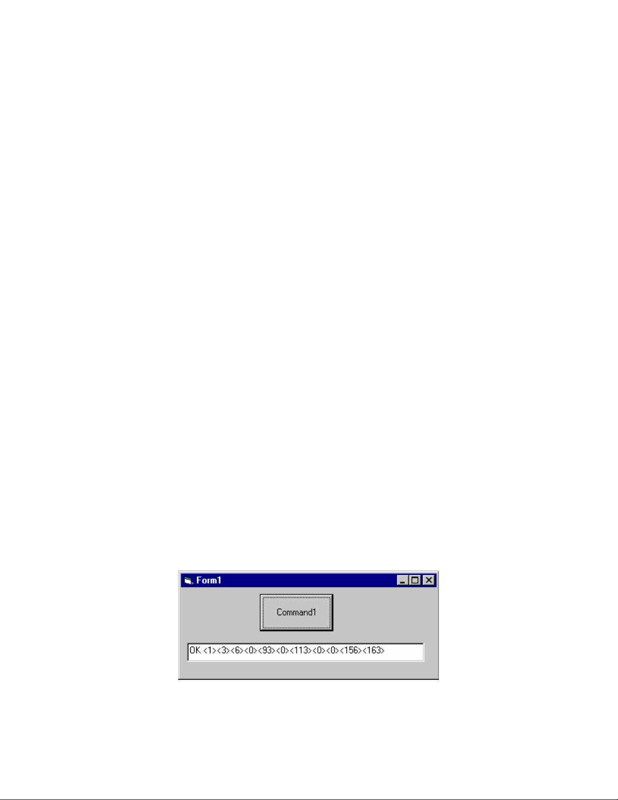
Chromalox Instruments and Controls
'can be calculated before the TxMessage is sent, when RxMessage contains
'the expected message length, then reception is complete.
'
'Check for valid message CRC:
RxCount = Len(RxMessage)
CRCValue = GetCRC(Mid(RxMessage, 1, RxCount - 2))
'compare result with received CRC:
If (CLng(Asc(Mid(RxMessage, RxCount - 1, 1))) + _
(CLng(Asc(Mid(RxMessage, RxCount, 1))) * 256)) = CRCValue Then
'CRC result matches OK (process data in RxMessage as needed)
Text1 = "OK "
'display values of message's data bytes:
For i = 1 To RxCount
Text1 = Text1 & "<" & Asc(Mid(RxMessage, i, 1)) & ">"
Next i
Else
'bad CRC result!
End If
End Select
End Sub
With the PC connected to a ProtocolTM Plus controller on COM1, and the controller is set for Address 1,
Baud Rate 38400, No Parity, clicking the command button produces the following display:
The data shows a good reply, with data values of 93, 113, and 0 for Holding Registers 16, 17, and 18,
respectively.
A-51643 Rev. 6 10/06/03 46
Page 53

Chromalox Instruments and Controls
7.2 Additional Communications Troubleshooting Hints
Communications problems occur primarily due to physical wiring problems or mismatched settings. It is
important to verify that the ProtocolTM Plus controller’s Communication Card is properly installed, and its
jumpers are properly set to match the wiring option used (RS-232, RS-422, or RS-485). Make sure the
controller has MODBUS communications enabled, and that communications is programmed to match the
controller’s Address, Baud Rate, and Parity settings.
For programming communications, make sure that the serial data format uses two stop bits as mentioned
above; using one stop bit will not work.
Programming should allow silent intervals between messages as described in the Modbus User’s guide, in
addition to transmitting bytes within a message continuously.
Finally, the ProtocolTM Plus controller requires that the “Communications Security Code”, Holding
Register 0, be properly set before accessing some registers via Modbus. A program may want to set this
register initially, with the Level 1 or 2 password associated with the controller, in order to avoid errors
trying to read critical registers later on.
Visual Basic is a trademark of Microsoft.
A-51643 Rev. 6 10/06/03 47
 Loading...