

Page 1

OLED DISPLAY MODULE
Application Notes
PRODUCT
NUMBER
DD-6448BE-2A with EVK board
Copyright ©2007 DENSITRON TECHNOLOGIES plc. All rights reserved. – Proprietary Data
Page 2

TABLE OF CONTENTS
1 EVK SCHEMATIC..........................................................................................................4
2 SYMBOL DEFINITION .................................................................................................5
3 TIMING CHARACTERISTICS ....................................................................................6
4 HOW TO USE THE SSD1305Z.................................................................................... 12
5 HOW TO USE THE DD-6448BE-2A...........................................................................13
5.1 R
ECOMMENDED INITIAL CODE .................................................................................. 14
6 WRITE DATA & COMMAND SUB FUNCTION..................................................... 16
Product No.
Copyright ©2007 DENSITRON TECHNOLOGIES plc. All rights reserved. – Proprietary Data
DD-6448BE-2A REV. A
Page 2 / 16
Page 3

REVISION RECORD
Rev. Date Page Chapt. Comment ECR no.
A 4th Sep 2007 First Issue
Product No.
Copyright ©2007 DENSITRON TECHNOLOGIES plc. All rights reserved. – Proprietary Data
DD-6448BE-2A REV. A
Page 3 / 16
Page 4

1 EVK Schematic
Product No.
Copyright ©2007 DENSITRON TECHNOLOGIES plc. All rights reserved. – Proprietary Data
DD-6448BE-2A REV. A
Page 4 / 16
Page 5

2 Symbol Definition
VCC : Power supply for panel driving voltage.
VSS:This is ground pin.
VDD:Power supply for core logic operation.
VDDIO:Power supply for interface logic level.
BS0~BS2:MUC bus interface selection pin(BS0 pulled LOW in internal).
CS:This pin is chip select input(active LOW).
RES:This pin is reset signal input(active LOW).
D/C:This is DATA/COMMAND control pin. When it is Pulled HIGH, the data at D[0~7] is
treated as data. When it is pulled LOW, the data at D[0~7] will be transferred to the command
register. In I2C mode, this pin acts as SA0 for slave address select.
R/W:This is read/write control input pin connecting to the MCU interface. When
interface to a 6800-series microprocessor , Read mode will be carried out when this pin is
pulled HIGH and write mode when low . When interface to an 8080-microprocessor , this
pin when be the data Write input. When serial interface is selected, this pin must be
connected to Vss.
E/RD:When interface to a 6800-series microprocessor , this pin will be used as the
Enable(E) signal. When interface to an 8080-microprocessor , this pin receives the
Read(RD#)signal.
D0~D7:These are 8-bit bi-directional data bus to be connected to the microprocessor’s data
bus. When serial interface mode is selected, D0(SCLK) will be the serial clock
input,D1(SDIN) will be the serial data input,D2 should be left opened. When I2C mode is
selected,D1(SDAin) AND D2(SDAout) should be tied together,D0(SCL) is the I2Cclock
input
IREF:This is segment output current reference pin.
VCOMH:This pin for COM signal deselected level voltage.
Product No.
Copyright ©2007 DENSITRON TECHNOLOGIES plc. All rights reserved. – Proprietary Data
DD-6448BE-2A REV. A
Page 5 / 16
Page 6

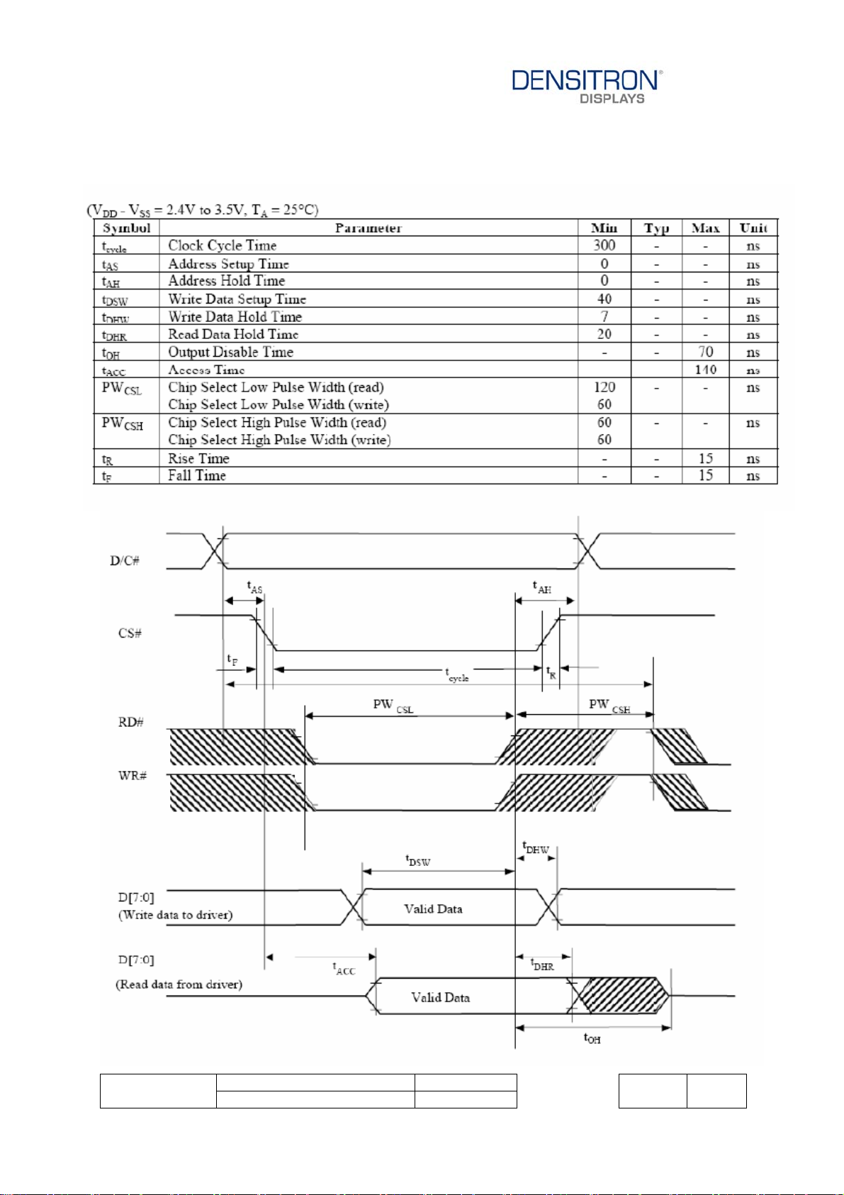
3 Timing characteristics
3.1.1 6800 Interfacing description and timing characteristics
Product No.
Copyright ©2007 DENSITRON TECHNOLOGIES plc. All rights reserved. – Proprietary Data
DD-6448BE-2A REV. A
Page 6 / 16
Page 7
3.1.2 8080 Interfacing descriptions and timing characteristics
Product No.
Copyright ©2007 DENSITRON TECHNOLOGIES plc. All rights reserved. – Proprietary Data
DD-6448BE-2A REV. A
Page 7 / 16
Page 8

3.1.3 SPI Interfacing and Descriptions Characteristics
Product No.
Copyright ©2007 DENSITRON TECHNOLOGIES plc. All rights reserved. – Proprietary Data
DD-6448BE-2A REV. A
Page 8 / 16
Page 9

3.1.4 I2C Interfacing and Descriptions Characteristics
Product No.
Copyright ©2007 DENSITRON TECHNOLOGIES plc. All rights reserved. – Proprietary Data
DD-6448BE-2A REV. A
Page 9 / 16
Page 10

Connection Between OLED and EVK
Figure 1 EVK PCB and DD-6448BE-2A Module
Figure 2 the DD-6448BE-2A and EVK assembled (Top view)
The SSD1305Z is a COG type package, that the connect pads are on top of the module
connector. When assembled the module and EVK push the locking pad to lock the module.
Product No.
Copyright ©2007 DENSITRON TECHNOLOGIES plc. All rights reserved. – Proprietary Data
DD-6448BE-2A REV. A
Page 10 / 16
Page 11

See Figure 1 and 2. The user can use the leading wire to connect EVK with the customers
application. The example is shown in Figure 3.
Figure 3 EVK with test platform.
Note 1:It is the external most positive voltage supply. In this sample is connected to power
supply.
Note 2: The leading wire has 13 pins totally in this case.
(D0~D7 – E/RD – R/W – D/C – RES – CS)
Note 3: Select Mode (8080 – 6800 – SPI – I2C)
Product No.
Copyright ©2007 DENSITRON TECHNOLOGIES plc. All rights reserved. – Proprietary Data
DD-6448BE-2A REV. A
Page 11 / 16
Page 12

4 How to use the SSD1305Z
4.1.1 Power down and Power up Sequence
To protect the OLED panel and extend the panel life time the driver IC power up/down
routine should include a delay period between high voltage and low voltage power sources
during turn off. Such that the panel has enough time to charge up or discharge before/after
operation.
Product No.
Copyright ©2007 DENSITRON TECHNOLOGIES plc. All rights reserved. – Proprietary Data
DD-6448BE-2A REV. A
Page 12 / 16
Page 13

play
5 How to use the DD-6448BE-2A
Reset Driver
IC
Product No.
Copyright ©2007 DENSITRON TECHNOLOGIES plc. All rights reserved. – Proprietary Data
DD-6448BE-2A REV. A
Driver IC
Initial Code
Display on
Clear RAM
Start
Dis
RES#=0; Delay 10ms; RES#=1
Suggest all registers set again
Page 13 / 16
Page 14

5.1 Recommended Initial code
void initial()
{
write_command(0x02);//set low column address
write_command(0x12);//set high column address
write_command(0x40);//(display start set)
write_command(0x2e);//(stop horzontal scroll)
write_command(0x81);//(set contrast control register)
write_command(0x32);
write_command(0x82);//(brightness for color banks)
write_command(0x80);//(display on)
write_command(0xa1);//(set segment re-map)
write_command(0xa6);//(set normal/inverse display)
write_command(0xa8);//(set multiplex ratio)
write_command(0x2F);
write_command(0xd3);//(set display offset)
write_command(0x40);
write_command(0xad);//(set dc-dc on/off)
write_command(0x8E);//
write_command(0xc8);//(set com output scan direction)
write_command(0xd5);//(set display clock divide ratio/oscillator/frequency)
write_command(0xf0);//
write_command(0xd8);//(set area color mode on/off & low power display mode )
write_command(0x05);//
write_command(0xd9);//(set pre-charge period)
write_command(0xF1);
write_command(0xda);//(set com pins hardware configuration)
write_command(0x12);
write_command(0xdb);//(set vcom deselect level)
Product No.
Copyright ©2007 DENSITRON TECHNOLOGIES plc. All rights reserved. – Proprietary Data
DD-6448BE-2A REV. A
Page 14 / 16
Page 15

write_command(0x34);
write_command(0x91);//(set look up table for area color)
write_command(0x3f);
write_command(0x3f);
write_command(0x3f);
write_command(0x3f);
write_command(0xaf);//(display on)
write_command(0xa4);//(display on)
}
Product No.
Copyright ©2007 DENSITRON TECHNOLOGIES plc. All rights reserved. – Proprietary Data
DD-6448BE-2A REV. A
Page 15 / 16
Page 16

6 WRITE DATA & COMMAND SUB FUNCTION
void write_command(unsigned char aa)
{
IOCLR = 0x000000ff;
IOSET = RD_IN;//RD=1
IOCLR = DC_IN;//RS=0
IOCLR = CS_IN;//CS=0
IOCLR = WR_IN;//W_R=0
IOSET = aa;//--------input command
IOSET = WR_IN;//W=1
IOSET = CS_IN;//CS=1
IOCLR = RD_IN;
}
void write_data(unsigned char bb)
{
IOCLR = 0x000000ff;
IOSET = RD_IN;//RD=1
IOSET = DC_IN;//RS=1
IOCLR = CS_IN;//CS=0
IOCLR = WR_IN;//W_R=0
IOSET = bb; //--------input data
IOSET = WR_IN;//W_R=1
IOSET = CS_IN;//CS_1=1
}
NOTE: RD recommended initial code and sub function for 8080 series CPU interface
Product No.
Copyright ©2007 DENSITRON TECHNOLOGIES plc. All rights reserved. – Proprietary Data
DD-6448BE-2A REV. A
Page 16 / 16
 Loading...