

Page 1
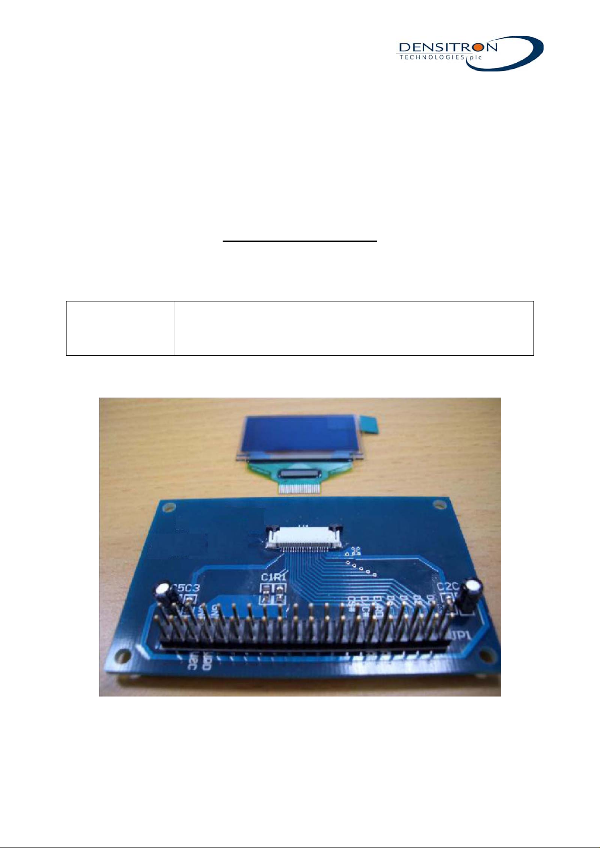
PRODUCT
NUMBER
OLED DISPLAY MODULE
Application Notes
DD-32645C-2A with EVK board
Copyright ©2006 DENSITRON TECHNOLOGIES plc. All rights reserved. – Proprietary Data
Page 2

TABLE OF CONTENTS
1 EVK SCHEMATIC..........................................................................................................4
2 SYMBOL DEFINITION ................................................................................................. 5
3 TIMING CHARACTERISTICS ....................................................................................6
4 CONNECTION BETWEEN OLED AND EVK ...........................................................7
5 HOW TO USE THE DD-32645C-2A .............................................................................9
5.1 RECOMMENDED INITIAL CODE .................................................................................. 10
Product No.
Copyright ©2005 DENSITRON TECHNOLOGIES plc. All rights reserved. – Proprietary Data
DD-32645C-2A REV. A
Page 2 / 11
Page 3

REVISION RECORD
Rev. Date Page Chapt. Comment ECR no.
A 21 Jun. 06 First Issue
Product No.
Copyright ©2005 DENSITRON TECHNOLOGIES plc. All rights reserved. – Proprietary Data
DD-32645C-2A REV. A
Page 3 / 11
Page 4

1 EVK Schematic
Product No.
Copyright ©2005 DENSITRON TECHNOLOGIES plc. All rights reserved. – Proprietary Data
DD-32645C-2A REV. A
Page 4 / 11
Page 5

2 Symbol Definition
Note: The EVK is hard wired to 8080 Parallel interface.
D0-D7:These pins are 8-bit bi-directional data bus to be connected to the MCU’s data bus.
E/RD#:This pin is MCU interface input. When connecting to an 8080-microprocessor, this
pin receives the Read (RD#) signal. Data read operation is initiated when this pin is pulled
low and the chip is selected.
R/W#:This pin is MCU interface input. When 8080 interface mode is selected, this pin will
be the Write (WR#) input. Data write operation is initiated when this pin is pulled low and the
chip is selected.
D/C#:This pin is Data/Command control pin. When the pin is pulled high, the data at D7-
D0 is treated as display data. When the pin is pulled low, the data at D7-D0 will be transferred
to the command register. For detail relationship to MCU interface signals, please refer to the
timing characteristics diagrams.
RES#:This pin is reset signal input. When the pin is low, initialization of the chip is executed.
CS#:This pin is the chip select input. The chip is enabled for MCU communication only when CS is
pulled low.
VCC:This is the most positive voltage supply pin of the chip.
VDD:Power supply pin for logic operation of the driver.
VSS:This is the ground pin and also acts as a reference for logic pins and OLED driving voltages.
This should be connected to the external ground
VCOMH:
should be connected between this pin and VSS.
NC:Dummy pad, do not group or short NC pins together.
This is an input pin for the voltage output high level for COM signals. A capacitor
Product No.
Copyright ©2005 DENSITRON TECHNOLOGIES plc. All rights reserved. – Proprietary Data
DD-32645C-2A REV. A
Page 5 / 11
Page 6

3 Timing characteristics
VDD = 2.4 to 3.5V, TA= -40to 85°C
Table 3 8080-Series MPU Parallel Interface Timing Characteristics
Figure 1 8080-series MPU parallel interface characteristics
Product No.
Copyright ©2005 DENSITRON TECHNOLOGIES plc. All rights reserved. – Proprietary Data
DD-32645C-2A REV. A
Page 6 / 11
Page 7

4 Connection Between OLED and EVK
Figure 2 EVK PCB and DD-32645C-2A Module
Figure 3 the DD-32645C-2A and EVK assembled (Top view)
Product No.
Copyright ©2005 DENSITRON TECHNOLOGIES plc. All rights reserved. – Proprietary Data
DD-32645C-2A REV. A
Page 7 / 11
Page 8

the connection pads are on top side.
When assemble the module with EVK. Just put the module in the connector and pull the
tenon to fix the module. See the Figure 3.
Figure 4 control MCU (not supplied) connected with EVK
Note 1:It is the external most positive voltage supply. In this sample is connected to power
supply.
Product No.
Copyright ©2005 DENSITRON TECHNOLOGIES plc. All rights reserved. – Proprietary Data
DD-32645C-2A REV. A
Page 8 / 11
Page 9

5 How to use the DD-32645C-2A
Product No.
Copyright ©2005 DENSITRON TECHNOLOGIES plc. All rights reserved. – Proprietary Data
DD-32645C-2A REV. A
Reset Set
RES#=0; Delay 10ms; RES#=1
Initial IC
code
Suggest all registers set again
Display on
Clear RAM
Start
sending
data
Page 9 / 11
Page 10

5.1 Recommended Initial code
void initial(void)
{
BS1=1; // use 8080 interface
BS2=1;
DC=0;
WR=0;
RD=0;
CS=0;
RES=0;
delay(100);
RES=1;
write_c(0xAE); //display off
write_c(0x81); //set contrast
write_c(0xff); //max current
write_c(0xa8); //set duty
write_c(0x3F); //duty 63
write_c(0xA0); //Set Segment Re-map
write_c(0xd3); //display offset
write_c(0x00); //set 00
write_c(0x40); //Start line
write_c(0xC8); //Set COM Output Scan Direction
write_c(0xda); //Set COM pins hardware configuration
write_c(0x12); //Set COM pins hardware configuration
write_c(0xD9); //Set precharge
write_c(0xf1); //precharge=fh , discharge=1h
write_c(0xDB); //Set VcomH
write_c(0x49); //VcomH=73
write_c(0xA4); //Normal Mode
write_c(0xA6); //No Inverse
write_c(0xAF); //display on
}
void write_c(unsigned char ins_c)
{
DC=0;
CS=0;
RD=1; /*tell system only write*/
WR=0;
d_bus=ins_c;
WR=1;
CS=1;
DC=1;
}
Product No.
Copyright ©2005 DENSITRON TECHNOLOGIES plc. All rights reserved. – Proprietary Data
DD-32645C-2A REV. A
Page 10 / 11
Page 11

void write_d(unsigned char ins_d)
{
DC=1;
CS=0;
RD=1; /*tell system only write*/
WR=0;
d_bus=ins_d;
CS=1;
WR=1;
DC=1;
}
void delay(int count)
{
int i,j;
for(i=0;i<=count;i++)
for(j=0;j<=1000;j++)
;
}
*write_c= Write Command , write_d= Write Data
Product No.
Copyright ©2005 DENSITRON TECHNOLOGIES plc. All rights reserved. – Proprietary Data
DD-32645C-2A REV. A
Page 11 / 11
Page 12

PRODUCT
NUMBER
OLED DISPLAY MODULE
Application Notes
DD-2864BY-2A with EVK board
Copyright ©2006 DENSITRON TECHNOLOGIES plc. All rights reserved. – Proprietary Data
Page 13

TABLE OF CONTENTS
1 EVK SCHEMATIC..........................................................................................................4
2 SYMBOL DEFINITION ................................................................................................. 5
3 TIMING CHARACTERISTICS ....................................................................................6
4 CONNECTION BETWEEN OLED AND EVK ........................................................... 7
5 HOW TO USE THE DD-2864BY-2A.............................................................................9
5.1 RECOMMENDED INITIAL CODE .................................................................................. 10
Product No.
Copyright ©2006 DENSITRON TECHNOLOGIES plc. All rights reserved. – Proprietary Data
DD-2864BY-2A
REV. A
Page 2 / 11
Page 14

REVISION RECORD
Rev. Date Page Chapt. Comment ECR no.
A 30-Augu-06 First Issue
Product No.
Copyright ©2006 DENSITRON TECHNOLOGIES plc. All rights reserved. – Proprietary Data
DD-2864BY-2A
REV. A
Page 3 / 11
Page 15

1 EVK Schematic
Product No.
Copyright ©2006 DENSITRON TECHNOLOGIES plc. All rights reserved. – Proprietary Data
DD-2864BY-2A
REV. A
Page 4 / 11
Page 16

2 Symbol Definition
Note: The EVK is hard wired to 8080 Parallel interface.
D0-D7:These pins are 8-bit bi-directional data bus to be connected to the MCU’s data bus.
RD#:This pin is MCU interface input. When connecting to an 8080-microprocessor, this pin
receives the Read (RD#) signal. Data read operation is initiated when this pin is pulled low
and the chip is selected.
WR#:This pin is MCU interface input. When 8080 interface mode is selected, this pin will
be the Write (WR#) input. Data write operation is initiated when this pin is pulled low and the
chip is selected.
D/C#:This pin is Data/Command control pin. When the pin is pulled high, the data at D7-
D0 is treated as display data. When the pin is pulled low, the data at D7-D0 will be transferred
to the command register. For detail relationship to MCU interface signals, please refer to the
timing characteristics diagrams.
RES#:This pin is reset signal input. When the pin is low, initialization of the chip is
executed.
CS#:This pin is the chip select input. The chip is enabled for MCU communication only
when CS is pulled low.
VCC:This is the most positive voltage supply pin of the chip.
VDD:Power Supply pin for logic operation of the driver.
VSS:This is a ground pin. It also acts as a reference for the logic pins and the OLED driving
voltages. It must be connected to external ground.
VCOMH:This is an input pin for the voltage output high level for COM signals. A
capacitor should be connected between this pin and VSS.
NC:Dummy pad. Do not group or short NC pins together.
Product No.
Copyright ©2006 DENSITRON TECHNOLOGIES plc. All rights reserved. – Proprietary Data
DD-2864BY-2A
REV. A
Page 5 / 11
Page 17

3 Timing characteristics
VDD = 2.4 to 3.5V, TA= -40to 85°C
Table 2 8080-Series MPU Parallel Interface Timing Characteristics
Figure 1 8080-series MPU parallel interface characteristics
Product No.
Copyright ©2006 DENSITRON TECHNOLOGIES plc. All rights reserved. – Proprietary Data
DD-2864BY-2A
REV. A
Page 6 / 11
Page 18

4 Connection Between OLED and EVK
Figure 2 EVK PCB and DD-2864BY-2A Module
Figure 3 the DD-2864BY-2A and EVK assembled (Top view)
Product No.
Copyright ©2006 DENSITRON TECHNOLOGIES plc. All rights reserved. – Proprietary Data
DD-2864BY-2A
REV. A
Page 7 / 11
Page 19

Figure 4 control MCU (not supplied) connected with EVK
Note 1:It is the external most positive voltage supply. In this sample is connected to power
supply.
Product No.
Copyright ©2006 DENSITRON TECHNOLOGIES plc. All rights reserved. – Proprietary Data
DD-2864BY-2A
REV. A
Page 8 / 11
Page 20

5 How to use the DD-2864BY-2A
Reset Set
RES#=0; Delay 10ms; RES#=1
Initial IC
code
Suggest all registers set again
Display on
Clear RAM
Start
sending
data
Product No.
Copyright ©2006 DENSITRON TECHNOLOGIES plc. All rights reserved. – Proprietary Data
DD-2864BY-2A
REV. A
Page 9 / 11
Page 21

5.1 Recommended Initial code
void initial(void)
{
BS1=1; // use 8080 interface
BS2=1;
DC=0;
WR=0;
RD=0;
CS=0;
RES=0;
delay(100);
RES=1;
write_c(0xAE); //display off
write_c(0x81); //set contrast
write_c(0xff); //max current
write_c(0xa8); //set duty
write_c(0x3F); //duty 63
write_c(0xA0); //Set Segment Re-map
write_c(0xd3); //display offset
write_c(0x00); //set 00
write_c(0x40); //Start line
write_c(0xC8); //Set COM Output Scan Direction
write_c(0xda); //Set COM pins hardware configuration
write_c(0x12); //Set COM pins hardware configuration
write_c(0xD9); //Set precharge
write_c(0xf1); //precharge=fh , discharge=1h
write_c(0xDB); //Set VcomH
write_c(0x49); //VcomH=73
write_c(0xA4); //Normal Mode
write_c(0xA6); //No Inverse
write_c(0xAF); //display on
}
void write_c(unsigned char ins_c)
{
DC=0;
CS=0;
RD=1; /*tell system only write*/
WR=0;
d_bus=ins_c;
WR=1;
CS=1;
DC=1;
}
Product No.
DD-2864BY-2A
REV. A
Page 10 / 11
Copyright ©2006 DENSITRON TECHNOLOGIES plc. All rights reserved. – Proprietary Data
Page 22

void write_d(unsigned char ins_d)
{
DC=1;
CS=0;
RD=1; /*tell system only write*/
WR=0;
d_bus=ins_d;
CS=1;
WR=1;
DC=1;
}
void delay(int count)
{
int i,j;
for(i=0;i<=count;i++)
for(j=0;j<=1000;j++)
;
}
*write_c= Write Command , write_d= Write Data
Product No.
DD-2864BY-2A
REV. A
Page 11 / 11
Copyright ©2006 DENSITRON TECHNOLOGIES plc. All rights reserved. – Proprietary Data
Page 23

PRODUCT
NUMBER
OLED DISPLAY MODULE
Application Notes
DD-2832BE-2A with EVK board
Copyright ©2006 DENSITRON TECHNOLOGIES plc. All rights reserved. – Proprietary Data
Page 24

TABLE OF CONTENTS
1 EVK SCHEMATIC..........................................................................................................4
2 SYMBOL DEFINITION ................................................................................................. 5
3 TIMING CHARACTERISTICS ....................................................................................6
4 CONNECTION BETWEEN OLED AND EVK ...........................................................7
5 HOW TO USE THE DD-2832BE-2A............................................................................. 9
5.1 RECOMMENDED INITIAL CODE .................................................................................. 10
Product No.
Copyright ©2005 DENSITRON TECHNOLOGIES plc. All rights reserved. – Proprietary Data
DD-2832BE-2A
REV. A
Page 2 / 11
Page 25

REVISION RECORD
Rev. Date Page Chapt. Comment ECR no.
A 20-June-06 First Issue
Product No.
Copyright ©2005 DENSITRON TECHNOLOGIES plc. All rights reserved. – Proprietary Data
DD-2832BE-2A
REV. A
Page 3 / 11
Page 26

1 EVK Schematic
Product No.
Copyright ©2005 DENSITRON TECHNOLOGIES plc. All rights reserved. – Proprietary Data
DD-2832BE-2A
REV. A
Page 4 / 11
Page 27

2 Symbol Definition
Note: The EVK is hard wired to 8080 Parallel interface.
D0-D7:These pins are 8-bit bi-directional data bus to be connected to the MCU’s data bus.
E/RD#:This pin is MCU interface input. When connecting to an 8080-microprocessor, this
pin receives the Read (RD#) signal. Data read operation is initiated when this pin is pulled
low and the chip is selected.
R/W#:This pin is MCU interface input. When 8080 interface mode is selected, this pin will
be the Write (WR#) input. Data write operation is initiated when this pin is pulled low and the
chip is selected.
D/C#:This pin is Data/Command control pin. When the pin is pulled high, the data at D7-
D0 is treated as display data. When the pin is pulled low, the data at D7-D0 will be transferred
to the command register. For detail relationship to MCU interface signals, please refer to the
timing characteristics diagrams.
RES#:This pin is reset signal input. When the pin is low, initialization of the chip is
executed.
CS#:This pin is the chip select input. The chip is enabled for MCU communication only
when CS is pulled low.
VCC:This is the most positive voltage supply pin of the chip.
VDD:Power Supply pin for logic operation of the driver.
VSS:This is a ground pin. It also acts as a reference for the logic pins and the OLED driving
voltages. It must be connected to external ground.
VCOMH:This is an input pin for the voltage output high level for COM signals. A
capacitor should be connected between this pin and VSS.
NC:Dummy pad. Do not group or short NC pins together.
Product No.
Copyright ©2005 DENSITRON TECHNOLOGIES plc. All rights reserved. – Proprietary Data
DD-2832BE-2A
REV. A
Page 5 / 11
Page 28

3 Timing characteristics
VDD = 2.4 to 3.5V, TA= -40to 85°C
Table 2 8080-Series MPU Parallel Interface Timing Characteristics
Figure 1 8080-series MPU parallel interface characteristics
Product No.
Copyright ©2005 DENSITRON TECHNOLOGIES plc. All rights reserved. – Proprietary Data
DD-2832BE-2A
REV. A
Page 6 / 11
Page 29

4 Connection Between OLED and EVK
Figure 2 EVK PCB and DD-2832BE-2A Module
Figure 3 the DD-2832BE-2A and EVK assembled (Top view)
Product No.
Copyright ©2005 DENSITRON TECHNOLOGIES plc. All rights reserved. – Proprietary Data
DD-2832BE-2A
REV. A
Page 7 / 11
Page 30

Figure 4 control MCU (not supplied ) connected with EVK
Note 1:It is the external most positive voltage supply. In this sample is connected to power
supply.
Product No.
Copyright ©2005 DENSITRON TECHNOLOGIES plc. All rights reserved. – Proprietary Data
DD-2832BE-2A
REV. A
Page 8 / 11
Page 31

5 How to use the DD-2832BE-2A
Reset Set
RES#=0; Delay 10ms; RES#=1
Initial IC
code
Suggest all registers set again
Display on
Clear RAM
Start
sending
data
Product No.
Copyright ©2005 DENSITRON TECHNOLOGIES plc. All rights reserved. – Proprietary Data
DD-2832BE-2A
REV. A
Page 9 / 11
Page 32

5.1 Recommended Initial code
void initial(void)
{
BS1=1; // use 8080 interface
BS2=1;
DC=0;
WR=0;
RD=0;
CS=0;
RES=0;
delay(100);
RES=1;
write_c(0xAE); //display off
write_c(0x81); //set contrast
write_c(0xff); //max current
write_c(0xa8); //set duty
write_c(0x1F); //duty 31
write_c(0xA0); //Set Segment Re-map
write_c(0xd3); //display offset
write_c(0x20); //set 32
write_c(0x40); //Start line
write_c(0xC8); //Set COM Output Scan Direction
write_c(0xda); //Set COM pins hardware configuration
write_c(0x12); //Set COM pins hardware configuration
write_c(0xD9); //Set precharge
write_c(0xf1); //precharge=fh , discharge=1h
write_c(0xDB); //Set VcomH
write_c(0x49); //VcomH=73
write_c(0xA4); //Normal Mode
write_c(0xA6); //No Inverse
write_c(0xAF); //display on
}
void write_c(unsigned char ins_c)
{
DC=0;
CS=0;
RD=1; /*tell system only write*/
WR=0;
d_bus=ins_c;
WR=1;
CS=1;
DC=1;
}
Product No.
DD-2832BE-2A
REV. A
Page 10 / 11
Copyright ©2005 DENSITRON TECHNOLOGIES plc. All rights reserved. – Proprietary Data
Page 33

void write_d(unsigned char ins_d)
{
DC=1;
CS=0;
RD=1; /*tell system only write*/
WR=0;
d_bus=ins_d;
CS=1;
WR=1;
DC=1;
}
void delay(int count)
{
int i,j;
for(i=0;i<=count;i++)
for(j=0;j<=1000;j++)
;
}
*write_c= Write Command , write_d= Write Data
Product No.
DD-2832BE-2A
REV. A
Page 11 / 11
Copyright ©2005 DENSITRON TECHNOLOGIES plc. All rights reserved. – Proprietary Data
 Loading...