

Page 1
For U.S.A. & Canada model
SERVICE MANUAL
MODEL DVM1835
DVD VIDEO AUTO CHANGER
Ver. 2
Pleas e refer t o the
MODIFICATION NOTICE.
●
For purposes of improvement, specifications and
design are subject to change without notice.
●
Please use this service manual with referring to the
operating instructions without fail.
●
Some illustrations using in this service manual are
slightly different from the actual set.
注 意
サービスをおこなう前に、このサービスマニュアルを
必ずお読みください。本機は、火災、感電、けがなど
に対する安全性を確保するために、さまざまな配慮を
おこなっており、また法的には「電気用品安全法」に
もとづき、所定の許可を得て製造されております。
従ってサービスをおこなう際は、これらの安全性が維
持されるよう、このサービスマニュアルに記載されて
いる注意事項を必ずお守りください。
●
本機の仕様は性能改良のため、予告なく変更すること
があります。
●
補修用性能部品の保有期間は、製造打切後8年です。
●
修理の際は、必ず取扱説明書を参照の上、作業を行っ
てください。
●
本文中に使用しているイラストは、説明の都合上現物
と多少異なる場合があります。
TOKYO, JAPAN
Denon Brand Company, D&M Holdings Inc.
X0289V.02 DE/CDM 0605
Page 2
SAFETY PRECAUTIONS
The following check should be performed for the continued protection of the customer and service technician.
LEAKAGE CURRENT CHECK
Before returning the unit to the customer, make sure you make either (1) a leakage current check or (2) a line to chassis
resistance check. If the leakage current exceeds 0.5 milliamps, or if the resistance from chassis to either side of the power
cord is less than 460 kohms, the unit is defective.
LASER RADIATION
Do not stare into beam or view directly with optical instruments, class 3A laser product.
DVM1835
CAUTION
Please heed the points listed below during servicing and inspection.
◎ Heed the cautions!
Spots requiring particular attention when servicing, such as
the cabinet, parts, chassis, etc., have cautions indicated on
labels or seals. Be sure to heed these cautions and the cautions indicated in the handling instructions.
◎ Caution concerning electric shock!
(1) An AC voltage is impressed on this set, so touching inter-
nal metal parts when the set is energized could cause
electric shock. Take care to avoid electric shock, by for example using an isolating transformer and gloves when
servicing while the set is energized, unplugging the power
cord when replacing parts, etc.
(2)There are high voltage parts inside. Handle with extra care
when the set is energized.
◎
Caution concerning disassembly and assembly!
Though great care is taken when manufacturing parts from
sheet metal, there may in some rare cases be burrs on the
edges of parts which could cause injury if fingers are moved
across them. Use gloves to protect your hands.
◎ Only use designated parts!
The set's parts have specific safety properties (fire resistance, voltage resistance, etc.). For replacement parts, be
sure to use parts which have the same properties. In particular, for the important safety parts that are marked ! on wiring
diagrams and parts lists, be sure to use the designated parts.
◎ Be sure to mount parts and arrange the
wires as they were originally!
For safety reasons, some parts use tape, tubes or other insulating materials, and some parts are mounted away from the
surface of printed circuit boards. Care is also taken with the
positions of the wires inside and clamps are used to keep
wires away from heating and high voltage parts, so be sure to
set everything back as it was originally.
◎ Inspect for safety after servicing!
Check that all screws, parts and wires removed or disconnected for servicing have been put back in their original positions, inspect that no parts around the area that has been
serviced have been negatively affected, conduct an insulation
check on the external metal connectors and between the
blades of the power plug, and otherwise check that safety is
ensured.
(Insulation check procedure)
Unplug the power cord from the power outlet, disconnect the
antenna, plugs, etc., and turn the power switch on. Using a
500V insulation resistance tester, check that the insulation resistance between the terminals of the power plug and the externally exposed metal parts (antenna terminal, headphones
terminal, microphone terminal, input terminal, etc.) is 1MΩ or
greater. If it is less, the set must be inspected and repaired.
CAUTION
Many of the electric and structural parts used in the set have
special safety properties. In most cases these properties are
difficult to distinguish by sight, and using replacement parts
with higher ratings (rated power and withstand voltage) does
not necessarily guarantee that safety performance will be preserved. Parts with safety properties are indicated as shown
below on the wiring diagrams and parts lists is this service
manual. Be sure to replace them with parts with the designated part number.
(1) Schematic diagrams ... Indicated by the ! mark.
(2) Parts lists ... Indicated by the ! mark.
Concerning important safety parts
Using parts other than the designated parts
could result in electric shock, fires or other
dangerous situations.
注 意
サービス、点検時にはつぎのことにご注意願います。
◎注意事項をお守りください!
サービスのとき特に注意を必要とする個所についてはキャ
ビネット、部品、シャーシなどにラベルや捺印で注意事項を
表示しています。これらの注意書きおよび取扱説明書などの
注意事項を必ずお守りください。
◎感電に注意!
(1) このセットは、交流電圧が印加されていますので通電時
に内部金属部に触れると感電することがあります。従っ
て通電サービス時には、絶縁トランスの使用や手袋の着
用、部品交換には、電源プラグを抜くなどして感電にご
注意ください。
(2) 内部には高電圧の部分がありますので、通電時の取扱に
は十分ご注意ください。
◎分解、組み立て作業時のご注意!
板金部品の端面の『バリ』は、部品製造時に充分管理をして
おりますが、板金端面は鋭利となっている箇所が有りますの
で、部品端面に触れたまま指を動かすとまれに怪我をする場
合がありますので十分注意して作業して下さい。手の保護の
ために手袋を着用してください。
◎指定部品の使用!
セットの部品は難燃性や耐電圧など安全上の特性を持った
ものとなっています。従って交換部品は、使用されていたも
のと同じ特性の部品を使用してください。特に配線図、部品
表に!印で指定されている安全上重要な部品は必ず指定の
ものをご使用ください。
◎部品の取付けや配線の引きまわしは、
元どおりに!
安全上、テープやチューブなどの絶縁材料を使用したり、プ
リント基板から浮かして取付けた部品があります。また内部
配線は引きまわしやクランパーによって発熱部品や高圧部
品に接近しないように配慮されていますので、これらは必ず
元どおりにしてください。
◎サービス後は安全点検を!
サービスのために取り外したねじ、部品、配線などが元どお
りになっているか、またサービスした個所の周辺を劣化させ
てしまったところがないかなどを点検し、外部金属端子部
と、電源プラグの刃の間の絶縁チェックをおこなうなど、安
全性が確保されていることを確認してください。
(絶縁チェックの方法)
電源コンセントから電源プラグを抜き、アンテナやプラグな
どを外し、電源スイッチを入れます。500V 絶縁抵抗計を用
いて、電源プラグのそれぞれの端子と外部露出金属部[アン
テナ端子、ヘッドホン端子マイク端子、入力端子など]との
間で、絶縁抵抗値が1 MΩ 以上であること、この値以下の
ときはセットの点検修理が必要です。
注 意
本機に使用している多くの電気部品、および機構部品は安全
上、特別な特性を持っています。この特性はほとんどの場合、
外観では判別つきにくく、またもとの部品より高い定格(定
格電力、耐圧)を持ったものを使用しても安全性が維持され
るとは、限りません。安全上の特性を持った部品は、この
サービスマニュアルの配線図、部品表につぎのように表示し
ていますので必ず指定されている部品番号のものを使用願
います。
(1) 配線図…!マークで表示しています。
(2) 部品表…!マークで表示しています。
安全上重要な部品について
指定された部品と異なるものを使用した場合に
は、感電、火災などの危険を生じる恐れがあり
ます。
2
Page 3

DVM1835
SPECIFICATIONS
Item Conditions Unit Nominal Limit
1. Video Output 75 Ω load Vpp 1.0 ± 0.1
2. Optical Digital Out dBm -18
3. Audio (PCM)
3-1. Output Level 1 kHz, 0 dB Vrms 2.0
3-2. S/N dB 120
3-3. Freq. Response
DVD fs = 48 kHz, 20 Hz ~ 22 kHz dB ± 0.5
CD fs = 44.1 kHz, 20 Hz ~ 20 kHz dB ± 0.5
3-4. THD+N
DVD 1 kHz, 0 dB % 0.003
CD 1 kHz, 0 dB % 0.003
Notes:
1. All Items are measured without pre-emphasis unless otherwise specified.
2. Power supply: AC 120 V, 60 Hz
3. Load Impedance: 100 kΩ load (Audio Output)
4. Room Ambient: 5 °C - 40 °C
3
Page 4
DVM1835
Safety Check after Servicing
Examine the area surrounding the repaired location for damage or deterioration. Observe that screws, parts, and
wires have been returned to their original positions. Afterwards, do the following tests and confirm the specified
values to verify compliance with safety standards.
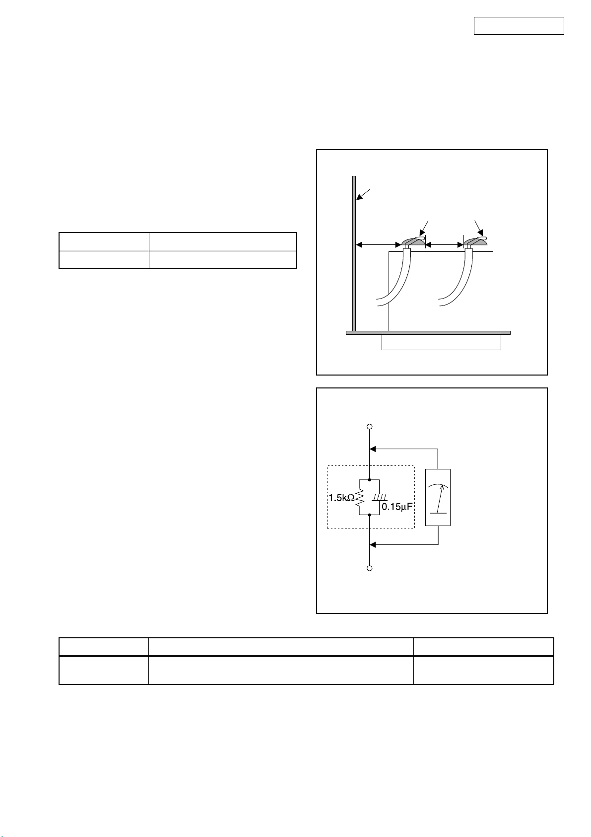
1. Clearance Distance
When replacing primary circuit components, confirm
specified clearance distance (d) and (d’) between
soldered terminals, and between terminals and
surrounding metallic parts. (See Fig. 1)
Table 1: Ratings for selected area
Chassis or Secondary Conductor
Primary Circuit
AC Line Voltage Clearance Distance (d), (d’)
120 V ≥ 3.2 mm (0.126 inches)
Note: This table is unofficial and for reference only. Be
sure to confirm the precise values.
2. Leakage Current Test
Confirm the specified (or lower) leakage current
between B (earth ground, power cord plug prongs) and
externally exposed accessible parts (RF terminals,
antenna terminals, video and audio input and output
terminals, microphone jacks, earphone jacks, etc.) is
lower than or equal to the specified value in the table
below.
Measuring Method (Power ON):
Insert load Z between B (earth ground, power cord plug
prongs) and exposed accessible parts. Use an AC
voltmeter to measure across the terminals of load Z.
See Fig. 2 and the following table.
d' d
Fig. 1
Exposed Accessible Part
Z
AC Voltmeter
(High Impedance)
Earth Ground
B
Power Cord Plug Prongs
Table 2: Leakage current ratings for selected areas
AC Line Voltage Load Z Leakage Current (i) Earth Ground (B) to:
120 V
Note: This table is unofficial and for reference only. Be sure to confirm the precise values.
0.15 µF CAP. & 1.5 kΩ RES.
Connected in parallel
i ≤ 0.5 mA Peak Exposed accessible parts
4
Fig. 2
Page 5
STANDARD NOTES FOR SERVICING
DVM1835
Circuit Board Indications
1. The output pin of the 3 pin Regulator ICs is
indicated as shown.
Top View
Out
2. For other ICs, pin 1 and every fifth pin are
indicated as shown.
Pin 1
3. The 1st pin of every male connector is indicated as
shown.
Pin 1
Input
In
Bottom View
5
10
Pb (Lead) Free Solder
When soldering, be sure to use the Pb free solder.
How to Remove / Install Flat Pack-IC
1. Removal
With Hot-Air Flat Pack-IC Desoldering Machine:
1. Prepare the hot-air flat pack-IC desoldering
machine, then apply hot air to the Flat Pack-IC
(about 5 to 6 seconds). (Fig. S-1-1)
Fig. S-1-1
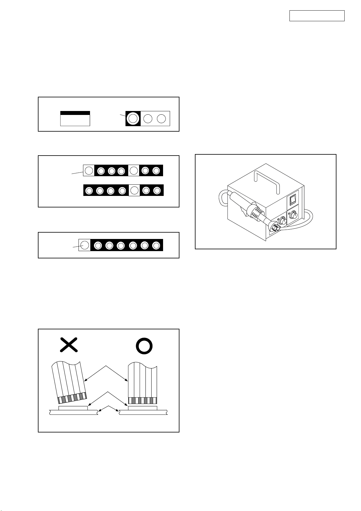
Instructions for Connectors
1. When you connect or disconnect the FFC (Flexible
Foil Connector) cable, be sure to first disconnect
the AC cord.
2. FFC (Flexible Foil Connector) cable should be
inserted parallel into the connector, not at an
angle.
FFC Cable
Connector
CBA
* Be careful to avoid a short circuit.
2. Remove the flat pack-IC with tweezers while
applying the hot air.
3. Bottom of the flat pack-IC is fixed with glue to the
CBA; when removing entire flat pack-IC, first apply
soldering iron to center of the flat pack-IC and heat
up. Then remove (glue will be melted). (Fig. S-1-6)
4. Release the flat pack-IC from the CBA using
tweezers. (Fig. S-1-6)
CAUTION:
1. The Flat Pack-IC shape may differ by models. Use
an appropriate hot-air flat pack-IC desoldering
machine, whose shape matches that of the Flat
Pack-IC.
2. Do not supply hot air to the chip parts around the
flat pack-IC for over 6 seconds because damage
to the chip parts may occur. Put masking tape
around the flat pack-IC to protect other parts from
damage. (Fig. S-1-2)
5
Page 6
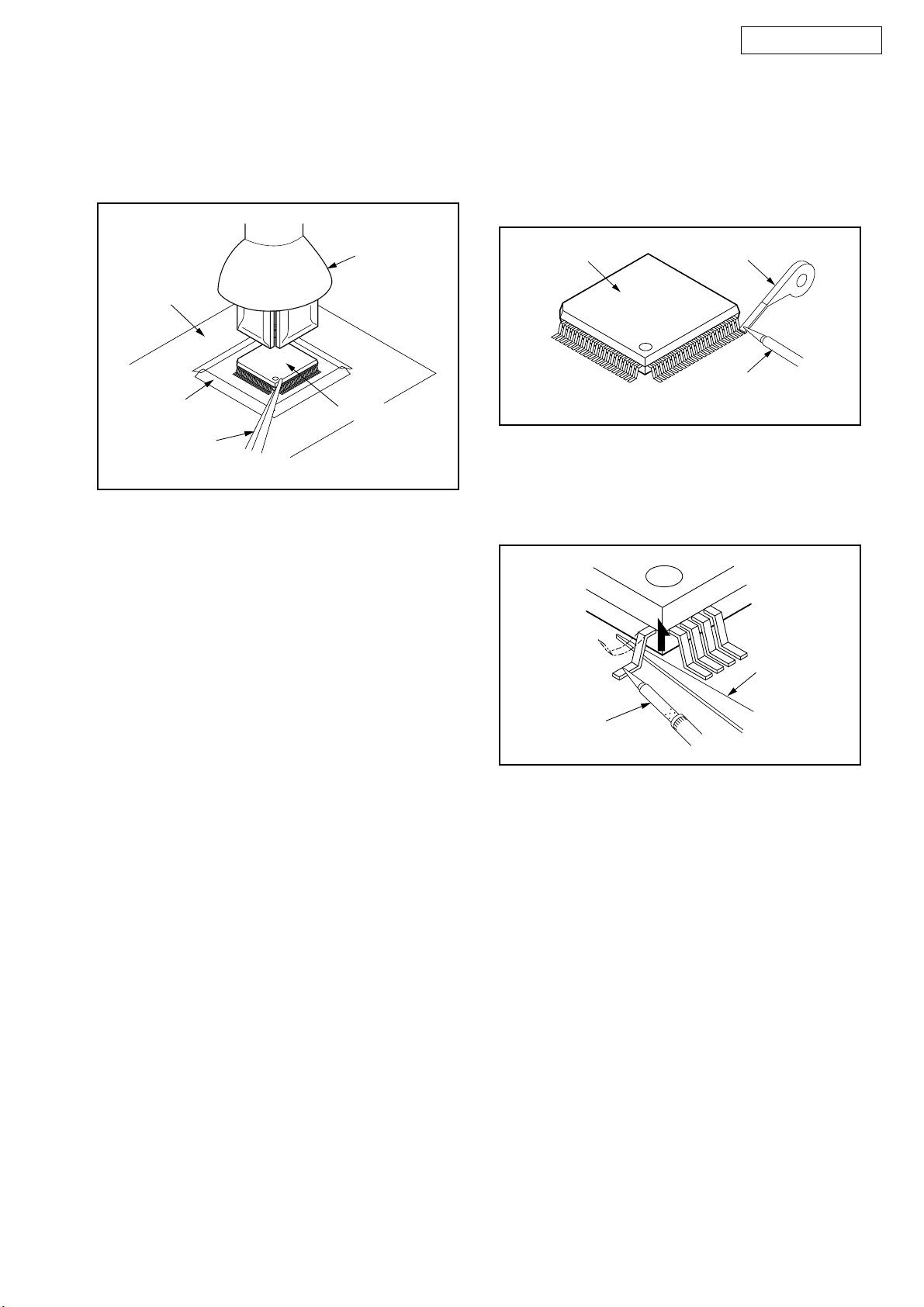
DVM1835
3. The flat pack-IC on the CBA is affixed with glue, so
be careful not to break or damage the foil of each
pin or the solder lands under the IC when
removing it.
Hot-air
Flat Pack-IC
Desoldering
CBA
Masking
Tape
Tweezers
Machine
Flat Pack-IC
Fig. S-1-2
With Soldering Iron:
1. Using desoldering braid, remove the solder from
all pins of the flat pack-IC. When you use solder
flux which is applied to all pins of the flat pack-IC,
you can remove it easily. (Fig. S-1-3)
Flat Pack-IC
2. Lift each lead of the flat pack-IC upward one by
one, using a sharp pin or wire to which solder will
not adhere (iron wire). When heating the pins, use
a fine tip soldering iron or a hot air desoldering
machine. (Fig. S-1-4)
Desoldering Braid
Soldering Iron
Fig. S-1-3
Sharp
Pin
Fine Tip
Soldering Iron
3. Bottom of the flat pack-IC is fixed with glue to the
CBA; when removing entire flat pack-IC, first apply
soldering iron to center of the flat pack-IC and heat
up. Then remove (glue will be melted). (Fig. S-1-6)
4. Release the flat pack-IC from the CBA using
tweezers. (Fig. S-1-6)
Fig. S-1-4
6
Page 7
DVM1835
With Iron Wire:
1. Using desoldering braid, remove the solder from
all pins of the flat pack-IC. When you use solder
flux which is applied to all pins of the flat pack-IC,
you can remove it easily. (Fig. S-1-3)
2. Affix the wire to a workbench or solid mounting
point, as shown in Fig. S-1-5.
3. While heating the pins using a fine tip soldering
iron or hot air blower, pull up the wire as the solder
melts so as to lift the IC leads from the CBA
contact pads as shown in Fig. S-1-5.
4. Bottom of the flat pack-IC is fixed with glue to the
CBA; when removing entire flat pack-IC, first apply
soldering iron to center of the flat pack-IC and heat
up. Then remove (glue will be melted). (Fig. S-1-6)
5. Release the flat pack-IC from the CBA using
tweezers. (Fig. S-1-6)
Note: When using a soldering iron, care must be
taken to ensure that the flat pack-IC is not
being held by glue. When the flat pack-IC is
removed from the CBA, handle it gently
because it may be damaged if force is applied.
Hot Air Blower
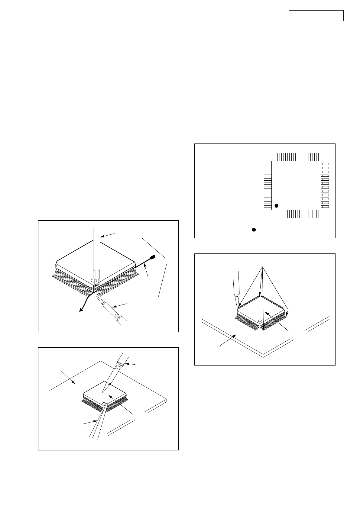
2. Installation
1. Using desoldering braid, remove the solder from
the foil of each pin of the flat pack-IC on the CBA
so you can install a replacement flat pack-IC more
easily.
2. The “●” mark on the flat pack-IC indicates pin 1.
(See Fig. S-1-7.) Be sure this mark matches the 1
on the PCB when positioning for installation. Then
presolder the four corners of the flat pack-IC. (See
Fig. S-1-8.)
3. Solder all pins of the flat pack-IC. Be sure that
none of the pins have solder bridges.
Example :
Pin 1 of the Flat Pack-IC
is indicated by a " " mark.
Fig. S-1-7
To Solid
Mounting Point
CBA
Tweezers
Iron Wire
Soldering Iron
Fig. S-1-5
Fine Tip
Soldering Iron
Flat Pack-IC
or
Presolder
Flat Pack-IC
CBA
Fig. S-1-8
Fig. S-1-6
7
Page 8
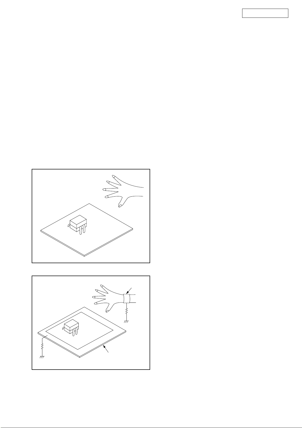
Instructions for Handling Semiconductors
Electrostatic breakdown of the semi-conductors may
occur due to a potential difference caused by
electrostatic charge during unpacking or repair work.
1. Ground for Human Body
Be sure to wear a grounding band (1 MΩ) that is
properly grounded to remove any static electricity that
may be charged on the body.
2. Ground for Workbench
Be sure to place a conductive sheet or copper plate
with proper grounding (1 MΩ) on the workbench or
other surface, where the semi-conductors are to be
placed. Because the static electricity charge on
clothing will not escape through the body grounding
band, be careful to avoid contacting semi-conductors
with your clothing.
DVM1835
<Incorrect>
<Correct>
CBA
Grounding Band
1MΩ
1MΩ
CBA
Conductive Sheet or
Copper Plate
8
Page 9
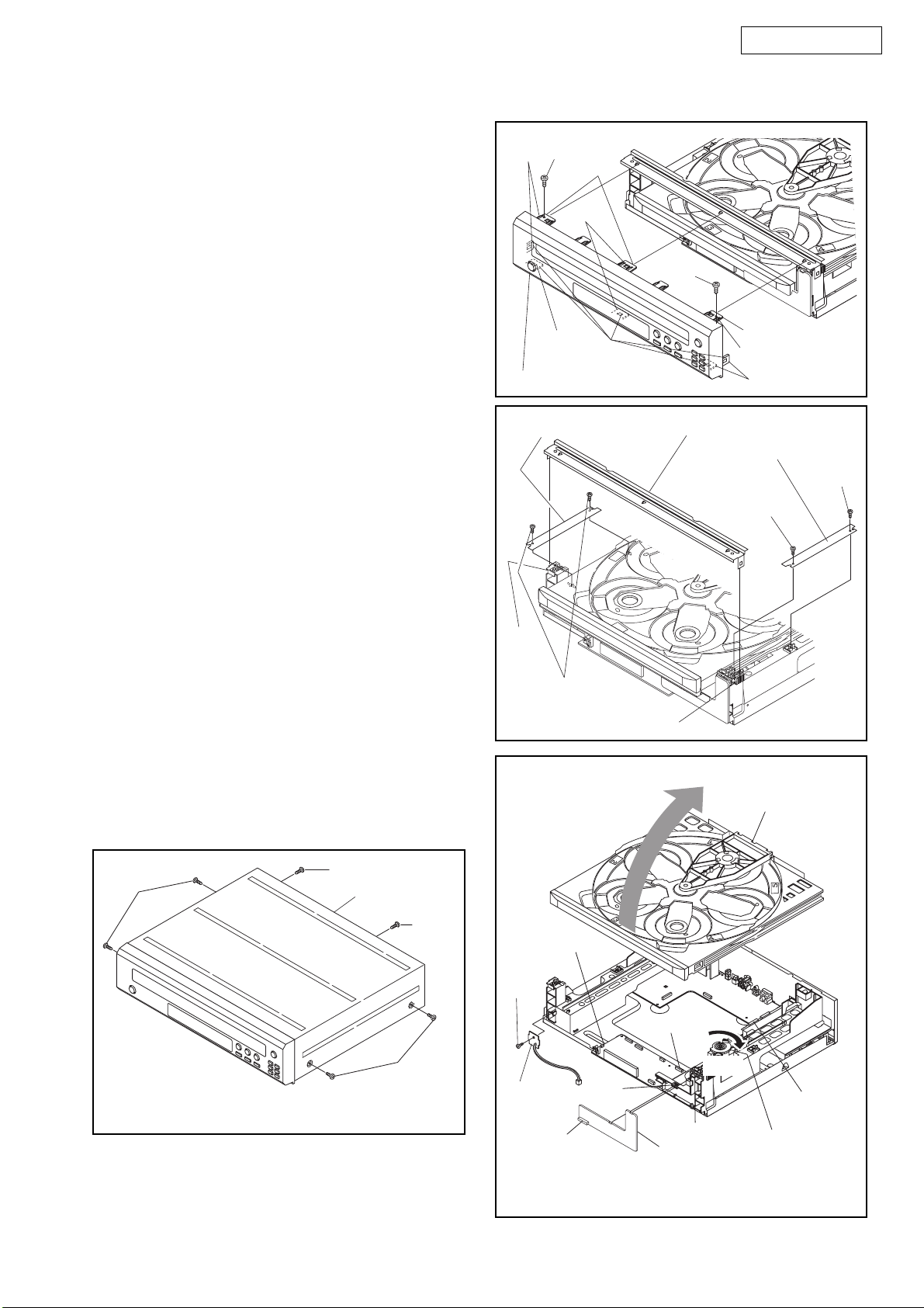
CABINET DISASSEMBLY INSTRUCTIONS
DVM1835
1. Disassembly Flowchart
This flowchart indicates the disassembly steps to gain
access to item(s) to be serviced. When reassembling,
follow the steps in reverse order. Bend, route, and
dress the cables as they were originally.
[1] Top Cover
[7] Power SW
CBA
[8] Relay CBA
[9] Sensor CBA
[13] Loading
Pulley
[14] Slide Tray
Gear (B)
[15] Slide Tray
Gear (A)
[16] Motor
Assembly
[17] Switch CBA
[18] Tray
Guide (R)
[6] Function CBA
[2] Front Assembly
[3] Bracket (Top)
[4] Stopper Bracket L, R
[5] Drive
Mechanism
[10] Rear Panel
[11] Tray Guide (L)
[12] Tray Guide
(R) Unit
[19] Changer CBA
[20] AV CBA
[21] Shield Plate
[22] DVD Main CBA Unit
[23] PCB Holder
2. Disassembly Method
ID/
LOC.
No.
PART
Fig.
No.
[1] Top Cover D1 6(S-1) -
Front
[2]
[3]
Assembly
Bracket
(Top)
D2 2(S-2), *8(L-1) 1-1
D3 *2(L-2) -
Stopper
[4]
Bracket
D3 4(S-3) -
L, R
REMOVAL
REMOVE/*UNHOOK/
UNLOCK/RELEASE/
UNPLUG/DESOLDER
Note
ID/
LOC.
No.
[5]
PART
Drive
Mechanism
REMOVE/*UNHOOK/
Fig.
UNLOCK/RELEASE/
No.
UNPLUG/DESOLDER
D4,
CN201, CN3001
D5
[6] Function CBA D4 *2(L-3), CN2201 -
REMOVAL
Power SW
[7]
CBA
[8] Relay CBA D6
Sensor
[9]
CBA
D4 CN2103, (S-4) -
2(S-5), CN5002,
CN5003, CN5005
D6 2(S-6) -
[10] Rear Panel D7 4(S-7), 11(S-8) -
Tr ay
[11]
Guide (L)
Tr ay
[12]
Guide (R)
Unit
Loading
[13]
Pulley
Slide Tray
[14]
Gear (B)
Slide Tray
[15]
Gear (A)
Motor
[16]
Assembly
Switch
[17]
CBA
Tr ay
[18]
Guide (R)
[19] Changer CBA D10
D8 3(S-9) -
4(S-10), CN3003,
D8
CN3004
D9 (S-11), Belt L -
D9 (S-12), *(P-1) -
D9 ---------- -
D9 (S-13) -
D9 *2(L-4) -
D9 ---------- -
CN3102, 2(S-14),
CN3301
6(S-15), CN1601,
[20] AV CBA D10
CN1001, FFC
Clamper
[21] Shield Plate D11 2(S-16), 2(W-1) -
DVD Main
[22]
CBA Unit
D11 2(S-17) -
[23] PCB Holder D11 (S-18) -
↓
(1)
↓
(2)
↓
(3)
↓
(4)
Note
2
2-1
3
4
-
-
-
-
↓
(5)
9
Page 10
(1): Identification (location) No. of parts in the figures
(2): Name of the part
(3): Figure Number for reference
(4): Identification of parts to be removed, unhooked,
unlocked, released, unplugged, unclamped, or
desoldered.
P=Spring, L=Locking Tab, S=Screw,
CN=Connector
*=Unhook, Unlock, Release, Unplug, or Desolder
e.g. 2(S-2) = two Screws (S-2),
2(L-2) = two Locking Tabs (L-2)
(5): Refer to “Reference Notes.”
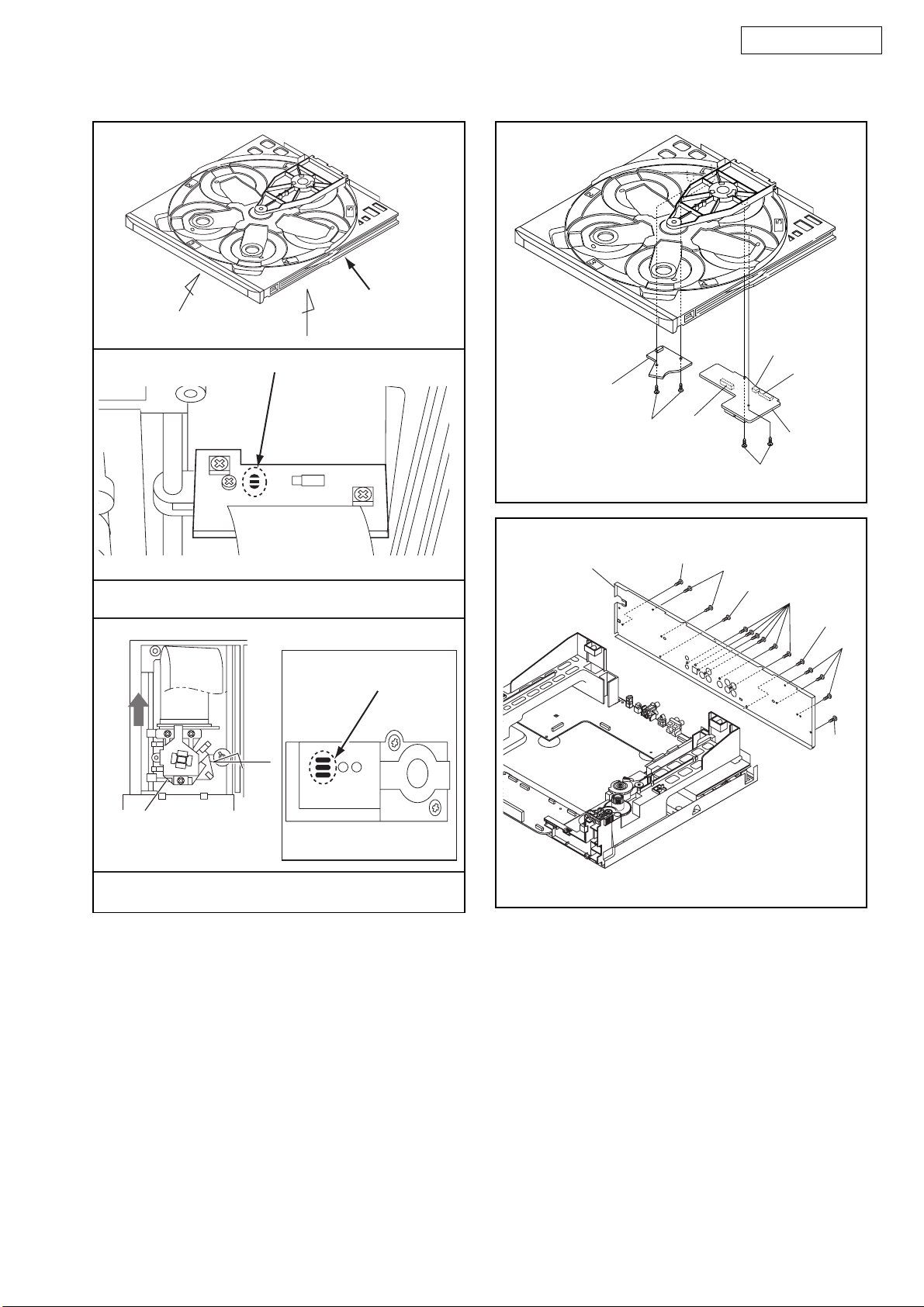
Reference Notes
CAUTION 1: Locking Tabs (L-1) are fragile. Be careful
not to break them.
1-1. To release eight Locking Tabs (L-1), first release
five Locking Tabs (A), and then three Locking
Tabs (B). (Fig. D2)
CAUTION 2: Electrostatic breakdown of the laser
diode in the optical system block may occur as a
potential difference caused by electrostatic charge
accumulated on cloth, human body etc., during
unpacking or repair work.
To avoid damage of pickup follow next procedures.
2-1. Short the three short lands of FPC cable with sol-
der before removing the FFC cable (CN201) from
it. If you disconnect the FFC cable (CN201), the
laser diode of pickup will be destroyed. (Fig. D5)
CAUTION 3: When reassembling, confirm the FFC
cable (CN201) is connected completely. Then remove
the solder from the three short lands of FPC cable.
(Fig. D5)
CAUTION 4: Before reinstalling, turn the Slide Tray
Gear (B) fully clockwise. (Fig. D4)
(S-2)
(L-1)
[2] Front Assembly
[4] Stopper Bracket L
(L-2)
(L-1)
(S-3)
(B)
(L-1)
(A)
(S-2)
[3] Bracket (Top)
[4] Stopper Bracket R
(L-2)
DVM1835
(L-1)
(B)
(L-1)
(S-3)
[5] Drive
Mechanism
Fig. D2
(S-3)
Fig. D3
(S-1)
(S-1)
[1] Top Cover
(S-1)
(S-1)
Fig. D1
10
CN2103
(S-4)
[7] Power
SW CBA
CN2201
(L-3)
CN3001
Turn
(L-3)
[6] Function CBA
CN201
Slide Tray
Gear (B)
Fig. D4
Page 11
DVM1835
Slide
A
Short the three short lands by soldering
Drive Mechanism
B
View for A
OR
Short the three short
lands by soldering
C
[9] Sensor CBA
[10] Rear Panel
(S-6)
CN5005
(S-7)
(S-8)
(S-5)
(S-7)
CN5003
CN5002
[8] Relay
CBA
Fig. D6
(S-8)
(S-7)
(S-8)
(S-7)
Pickup Unit
View for B
View for C
Fig. D5
Fig. D7
11
Page 12
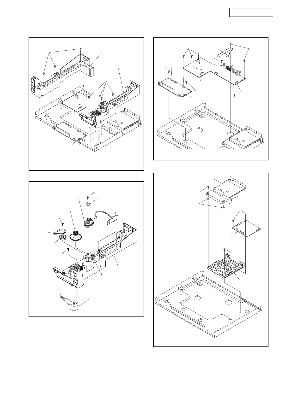
DVM1835
(S-9)
CN3003
CN3004
[11] Tray Guide (L)
[12] Tray Guide
(R) Unit
(S-10)
Fig. D8
CN3102
(S-14)
(S-15)
CN3301
CN1001
[19] Changer CBA
[21] Shield Plate
FFC
Clamper
(S-15)
(S-14)
(S-15)
CN1601
[20] AV CBA
Fig. D10
[14] Slide Tray Gear (B)
[15] Slide Tray Gear (A)
(S-11)
Belt L
[13] Loading
Pulley
(S-13)
(S-12)
(P-1)
[17] Switch CBA
[18] Tray
Guide (R)
(L-4)
[16] Motor Assembly
Fig. D9
(S-16)
(W-1)
[22]
DVD
Main CBA
Unit
(S-16)
(S-17)
(S-18)
[23] PCB
Holder
12
Fig. D11
Page 13
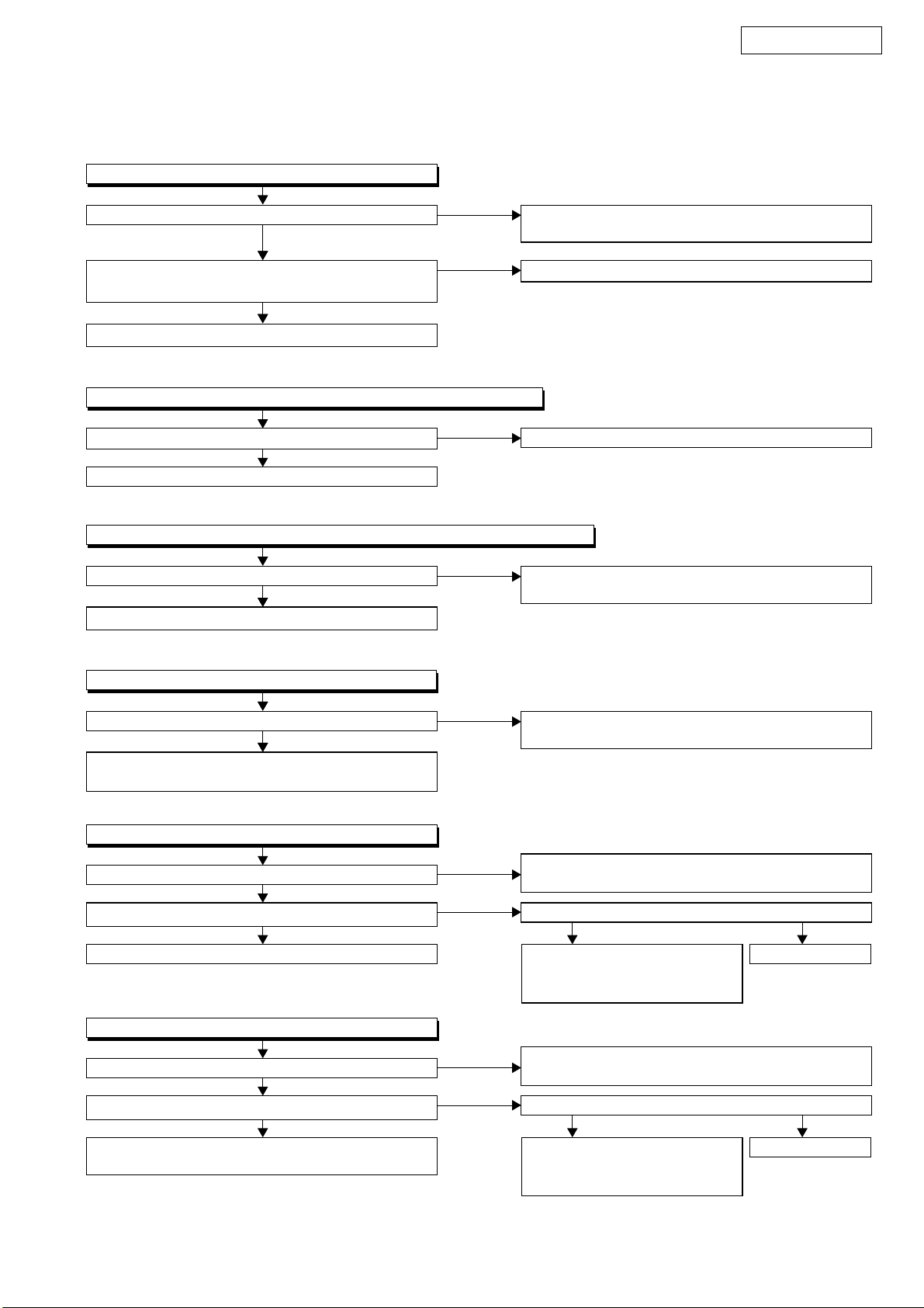
FLOW CHART NO.1
The power cannot be turned on.
DVM1835
TROUBLESHOOTING
Is the fuse normal?
Ye s
Is normal state restored when once unplugged
power cord is plugged again after several seconds?
Ye s
Is the EV +9V line voltage normal?
Ye s
Is each voltage of the secondary side normal?
Ye s
When pressing POWER button (SW2201), is the
voltage of 0V supplied to pin(38) of IC3001?
Ye s
Is the voltage of 3.3V supplied to pin(1) of IC3001?
Ye s
Replace IC3001.
FLOW CHART NO.2
The fuse blows out.
Check the presence that the primary component
is leaking or shorted and service it if defective.
No
No
No
No
No
No
See FLOW CHART No.2 <The fuse blows out.>
Check if there is any leak or shor-circuiting on the
primary circuit component, and service it if defective.
(Q1001, Q1003, T1001, D1001, D1002, D1004,
D1005, D1011, C1003, C1005)
Check each rectifying circuit of the secondary circuit
and service it if defective.
Check POWER button (SW2201) and their
periphery, and service it if defective.
Check CHG+3.3V line
See FLOW CHART No.2 <The fuse blows out.>
Check the presence that the rectifying diode or
circuit is shorted in each rectifying circuit of
secondary side, and service it if defective.
and service it if defective.
After servicing, replace the fuse.
FLOW CHART NO.3
When the output voltage fluctuates.
Does the photo coupler circuit on the secondary
side operate normally?
Ye s
Check IC1001, D1012, D1024 and their periphery,
and service it if defective.
FLOW CHART NO.4
When buzz sound can be heard in the vicinity of AV circuit.
Check if there is any short-circuit on the rectifying diode and the circuit in each rectifying circuit of the secondary side
and service it if defective.
FLOW CHART NO.5
-FL is not outputted.
Is -24V voltage supplied to the anode of D1003?
Check if there is any leak or short-circuit
on the loaded circuit, and service it if defective.
(D1003, D1006, D1008, D1016, D1030, IC1002, Q1002, Q1004, Q1010, Q1011, Q1014)
Ye s
No
No
Check IC1001, IC1006, D1015 and their
periphery, and service it if defective.
Check D1003 and periphery circuit, and service it
if defective.
,
13
Page 14
FLOW CHART NO.6
P-ON+9V (EV+9V) is not outputted.
DVM1835
Is 9V voltage supplied to the emitter of Q1002?
Ye s
Is the voltage of base on Q1002 lower than the
voltage of emitter on Q1002 when turning the power on?
Ye s
Replace Q1002.
FLOW CHART NO.7
P-ON+5V is not outputted. (P-ON+9V is outputted normally.)
Is the "H" signal inputted into the base of Q1004?
Ye s
Replace Q1004.
FLOW CHART NO.8
P-ON+3.3V is not outputted. (P-ON+9V is outputted normally.)
Is 3.3V voltage supplied to the collector of Q1011?
Ye s
Replace Q1011 and R1067.
No
No
No
No
Check D1030, C1035, C1048, L1009 and
the periphery circuit, and service it if defective.
Check Q1016 and service it if defective.
Check R1068 and D1046, and service it if defective.
Check D1008, D1015, C1007, C1038, L1007 and
the periphery circuit, and service it if defective.
FLOW CHART NO.9
EV+5V is not outputted.
Is EV+9V outputted normally?
Ye s
Check Q1014, D1047 and the periphery circuit,
and service it if defective.
FLOW CHART NO.10
EV+1.5V is not outputted.
Is 2.5V voltage supplied to Pin(1) of IC1002?
Ye s
Is 1.25V voltage supplied to Pin(4) of IC1002?
Ye s
Replace IC1002.
FLOW CHART NO.11
EV+3.3V is not outputted.
Is 3.3V voltage supplied to emitter of Q1010?
Ye s
Is the "L" signal inputted to base of Q1012?
Ye s
Check Q1010, Q1012, R1087 and R1088, and
service it if defective.
No
No
No
No
No
Refer to "FLOW CHART NO.6"
<P-ON+9V (EV+9V) is not outputted.>
Check D1006, C1014, C1050, L1008 and the
periphery circuit, and service it if defective.
Is the "L" signal outputted into Pin(8) of IC3001?
Ye s No
Check the circuit between Pin(8)
of IC3001 and Pin(4) of IC1002
and service it if defective.
Check D1008, D1015, C1007, C1038, L1007 and
the periphery circuit, and service it if defective.
Is the "L" signal outputted into Pin(8) of IC3001?
Ye s No
Check the circuit between Pin(8)
of IC3001 and base of Q1012
and service it if defective.
Replace IC3001.
,
Replace IC3001.
,
14
Page 15

FLOW CHART NO.12
SW
The fluorescent display tube does not light up.
DVM1835
Is 3.3V voltage supplied to Pin(6) and
Pin(24) of IC2001?
Ye s
Is the voltage of approximately -24V to -28V
supplied to Pin(15) of IC2001?
Ye s
Is there 500kHz oscillation at Pin(26) of IC2001?
Ye s
Are the filament voltage supplied between
Pins(1, 2) and Pins(34, 35) of the fluorescent
display tube? And the negative voltage applied
between these pins and GND?
Ye s
Replace the fluorescent display tube.
FLOW CHART NO.13
The key operation is not functioning.
No
No
No
No
Check the P-ON+3.3V line and service it if defective.
Check the -FL (-28V) line and service it if defective.
Check R2015, IC2001 and their periphery, and
service it if defective.
Check D1016, D1017, T1001, and their periphery,
and service it if defective.
No
Is -17V voltage supplied to collector of Q1005?
Ye s
Is the "H" signal inputted
to base of Q1016?
Check the EV+3.3V
line, and service
No
it if defective.
Ye s
Check Q1015, Q1016, D1055, and
their periphery, and service it if defective.
Are the contact point and the installation state of the
key switches (SW2201 - 2214) normal?
Terminal Voltage of Pins (38 - 42) on IC3001
0.00 - 0.50
0.51 - 1.53
1.54 - 2.57
2.58 - 3.30 (KEY OFF) (KEY OFF) (KEY OFF) (KEY OFF) (KEY OFF)
Ye s
Is the control voltage normally supplied to pins(38,
39, 40, 41, 42) of IC3001?
Ye s
Replace IC3001.
No
Re-install the switches (
SW2201 - 2214
correctly or replace the poor switch.
IC3001
38pin 39pin 40pin 41pin 42pin
KEY1 KEY2 KEY3 KEY4 KEY5
SW2201
POWER
SW2202
STOP
SW2203
PLAY
No
SW2204
SKIP DOWN
SW2205
SKIP UP
SW2206
SELECT
SW2207
DISC-5
SW2208
DISC-4
SW2209
OPEN/CLOSE
Check the switches (
SW2210
DISC-3
SW2211
DISC-2
SW2212
DISC-1
SW2201 - 2214
and their periphery, and service it if defective.
)
2213
STILL/PAUSE
EXTRA
-----
)
15
Page 16

FLOW CHART NO.14
No operation is possible from the remote control unit.
Operation is possible from the DVD, but no
operation is possible from the remote control unit.
Ye s
Is 5V voltage supplied to the Pin(3) terminal of
the infrared remote control receiver (RM2001)?
Ye s
Is the "L" pulse sent out Pin(1) terminal of receiver
(RM2001) when the infrared remote control is activated?
Ye s
Is the "L" pulse supplied to the Pin(6) of IC3001?
Ye s
Is the "L" pulse supplied to the Pin(22) of CN1001?
Ye s
Replace the DVD Main CBA Unit or DVD Mechanism.
No
No
No
No
DVM1835
Check EV+5V line and service it if defective.
Replace the infrared remote control receiver (RM2001).
Or replace the remote control unit.
Check the line between Pin(1) of RM2001 and
Pin(6) of IC3001, and service it if defective.
Check the line between Pin(1) of RM2001 and
Pin(22) of CN1001, and service it if defective.
FLOW CHART NO.15
The disc tray cannot be opened and closed. (It can be done using the remote control unit.)
Is the normal control voltage inputted to Pin(40) of
IC3001?
Ye s
Refer to "FLOW CHART NO.16" <The disc tray
cannot be opened and closed.>
FLOW CHART NO.16
The disc tray cannot be opened and closed.
Replace the DVD Main CBA Unit.
No improvement can be found.
Ye s
Replace the DVD Mechanism.
FLOW CHART NO.17
[No Disc] indicated. (When the focus error occurs.)
Replace the DVD Main CBA Unit.
No
No
Replace the "OPEN/CLOSE" button (SW2209).
Original DVD Main CBA Unit is poor.
No improvement can be found.
Ye s
Replace the DVD Mechanism.
No
Original DVD Main CBA Unit is poor.
16
Page 17

FLOW CHART NO.18
[No Disc] indicated. (When the focus servo is not functioning.)
Replace the DVD Main CBA Unit.
DVM1835
No improvement can be found.
Ye s
Replace the DVD Mechanism.
FLOW CHART NO.19
[No Disc] indicated. (When the laser beam does not light up.)
Replace the DVD Main CBA Unit.
No improvement can be found.
Ye s
Replace the DVD Mechanism.
FLOW CHART NO.20
Both functions of picture and sound do not operate normally.
Replace the DVD Main CBA Unit.
No improvement can be found.
Ye s
Replace the DVD Mechanism.
No
No
No
Original DVD Main CBA Unit is poor.
Original DVD Main CBA Unit is poor.
Original DVD Main CBA Unit is poor.
17
Page 18

FLOW CHART NO.21
Picture does not appear normally.
Set the disc on the disc tray, and playback.
DVM1835
Are the video signals outputted to each pin of
CN1601 on the AV CBA?
CN1601 3PIN Pr/Cr
CN1601 5PIN Pb/Cb
CN1601 7PIN S-Y(I/P)
CN1601 9PIN S-C
Ye s
Are the video signals shown above inputted into
each pin of IC1402?
IC1402 2PIN S-C
IC1402 6PIN S-Y(I/P)
IC1402 9PIN Pb/Cb
IC1402 11PIN Pr/Cr
Ye s
Are the video signals outputted to each pin
of IC1402?
IC1402 18PIN S-Y(I/P)
IC1402 15PIN Pb/Cb
IC1402 13PIN Pr/Cr
IC1402 21PIN CVBS
IC1402 23PIN S-C
Ye s
Are the video signals outputted to the specific
output terminal?
Are the luminance signals outputted to the
S-OUT terminal (JK1401)?
Are the chroma signals outputted to the
S-OUT terminal (JK1401)?
Are the component video signals outputted to the
VIDEO OUT terminal (JK1403)?
Are the composite video signals outputted to
the VIDEO OUT terminal (JK1403)?
No
No
No
No
No
No
No
Replace the DVD Main CBA Unit or DVD Mechanism.
Check the line between each pin of CN1601 and
each pin of IC1402 on the AV CBA, and service
it if detective.
CN1601 9PIN → IC1402 2PIN S-C
CN1601 7PIN → IC1402 6PIN S-Y(I/P)
CN1601 5PIN → IC1402 9PIN Pb/Cb
CN1601 3PIN → IC1402 11PIN Pr/Cr
Is 5V voltage applied to the Pin(1, 24) of IC1402 ?
Ye s N o
Replace IC1402.
Check the periphery of JK1401 from
Pin (18) of IC1402 and service it if detective.
Check the periphery of JK1401 from
Pin (23) of IC1402 and service it if detective.
Check the periphery of JK1403 from Pins (13, 15,
18) of IC1402 and service it if detective.
Check
the periphery of
IC1402
and service it if detective.
Check P-ON+5V line and
service it if detective.
JK1403 from Pin(21) of
18
Page 19

FLOW CHART NO.22
Audio is not outputted.
Set the disc on the disc tray, and playback.
DVM1835
Are the analog audio signals outputted to each pin
of CN1601 on AV CBA?
CN1601 13PIN AUDIO-L
CN1601 15PIN AUDIO-R
Ye s
Are the analog audio signals inputted to each pin
of IC1201.
IC1201 2PIN AUDIO-L
IC1201 6PIN AUDIO-R
Ye s
Is the "H" level mute signal outputted to CN1601
on AV CBA ?
CN1601 12PIN A-MUTE
CN1601 16PIN A-R-MUTE
CN1601 14PIN A-L-MUTE
Ye s
Are the analog audio signals inputted to each pin
of IC1201?
IC1201 1PIN AUDIO-L
IC1201 7PIN AUDIO-R
Ye s
Are the audio signals outputted to the specific
output terminal?
Are the audio signals outputted to the audio
terminal (JK1201)?
No
No
No
No
No
Replace the DVD Main CBA Unit or DVD Mechanism.
Check each line between each pin of CN1601
and each pin of IC1201 on AV CBA, and service it
if defective.
CN1601 13PIN → IC1201 2PIN AUDIO-L
CN1601 15PIN → IC1201 6PIN AUDIO-R
Replace the DVD Main CBA Unit or DVD Mechanism.
Replace IC1201.
Check the periphery between Pins(1,7) of IC1201
and JK1201, and service it if defective.
19
Page 20

FLOW CHART NO.23
Rotary tray does not function.
DVM1835
Is the normal control voltage inputted to pins
(39, 40, 41) of IC3001? For each terminal voltage,
refer to FLOW CHART No.13 <The key operation
is not functioning.>
Ye s
Is the voltage of 3.3V supplied to pin(1) of IC3001?
Ye s
Is the normal control voltage outputted to pins
(24, 25) of IC3001?
Ye s
Is the normal control voltage outputted to pins(2,4)
of IC3003?
Ye s
Replace Rotary Motor.
No
No
No
No
Check the switches (SW2206 - 2208, 2210 - 2212)
and their periphery, and service it if defective.
Check CHG 3.3V line and service it if detective.
Replace IC3001.
Is the voltage of 9V supplied to pin(6) of IC3003?
Ye s
Replace IC3003.
Check EV+9V line and
service it if detective.
No
20
Page 21

BLOCK DIAGRAMS
System Control / Servo Block Diagram
SEGMENT
FIP
GRID
FL2001
~
FRONT
IC2001
789
12
1011131416
efg
i
h
VFD-STB
VFD-DIN
VFD-DOUT
VFD-CLK
2
1
28
27
343637
35
VFD-DIN
VFD-STB
VFD-CLK
VFD-DOUT
a
bcd
~
23 17
1G 7G
PANEL
CONTROL
DVM1835
D2201
KEY SWITCH
FUNCTION CBA
CN2201CN2101
2 KEY-1 2
3 KEY-2 3
4 KEY-3 4
5 KEY-4 5
6 KEY-5
3839404142
KEY-1
KEY-2
KEY-3
KEY-4
KEY-5 6
POWER
SW2201
CN2203CN2103
1 KEY-1 1
STANDBY
POWER
SWITCH CBA
3
STANDBY-LED
2 GND 2
3
23
SENSOR
REMOTE
RM2001
STANDBY-LED
(CH MICROPROCESSOR)
IC3001
CHANGER CBA
+3.3V
ST-OP/CL
30
IC3004 (LOADING MOTOR DRIVE)
FP-RIN
FP-FIN
13
14
Q3005
971
CONTROL
LOGIC
DRIVE
4
2
ST-GAIN
31
AMP
IC3003 (ROTARY MOTOR DRIVE)
CN5001 CN3001
RT-RIN
RT-FIN
242526
Q3004
971
CONTROL
LOGIC
DRIVE
4
2
7 RM2 7
5 RM1 5
RT-GAIN
AMP
Q3002
CN5001 CN3001
D-SENS-A
4
Q3003
+3.3V
8 D-SENS-A 8
6 RT-SENS-A 6
RT-SENS-A
5
CN5001 CN3001
CHK-ON
32
1 CHK-ON 1
3 CHK-OFF 3
FP-STB
FP-DIN
FP-DOUT
FP-CLK
REMOTE
7
6
121110
11 FP-STB 11
12 FP-DIN 12
13 FP-DOUT 13
14 FP-CLK 14
16 REMOTE2 16
CN1102
AV CBA
16 FP-STB 16
18 FP-DIN 18
20 FP-DOUT 20
21 FP-CLK 21
22 REMOTE1 22
CN401 CN1001 CN3102
59
54
55
61
53
FP-DIN
FP-STB
FP-CLK
FP-DOUT
REMOTE1
(MICRO CONTROLLER)
EXT CLOCK
CLK33M
BE CLOCK
IC101
92
172
170
36.864MHz
X451
7
X'TAL
MULTI
IC451 (CLOCK GENERATOR)
RELAY CBA
FSEL
FOCUS
(SERVO DRIVE)
IC301
27
-
+
+
FOCUS
ACTUATOR
15
FS(+)
152
26
-
FS(-)
DRIVE
25
DRIVE
16
TS(+)
17
OSC
8
14
OSC
PLL
1/4
1/4 PLL2
3
15
10
24
TS(-)
REMOTE2
REMOTE1
TRACKING
DRIVE
150
123
-
+
-
+
TRACKING
ACTUATOR
DRIVE
14
13
TO
VIDEO/ AUDIO
SPINDLE
BLOCK DIAGRAM
SPDL
71
4
-
+
+-+
MOTOR
DRIVE
12
11
CN301CN5001CN5003
SLD
70
6235
-
SLED
MOTOR
DRIVE
17
18
3SP(+)
4SP(-)
8SL(-)
34891 FG-IN
9SL(+)
IC461
1
A-MUTE
ADAC-MD
86
A-MUTE
IC202
Q3006
TO
VIDEO/ AUDIO
BLOCK DIAGRAM
ADAC-ML
ADAC-MC
51
50
ADAC-MD
ADAC-MC
RESET68
RESET
5 4
+3.3V
(OP AMP)
87
ADAC-ML
FG-IN
66
12 14
DVD MAIN CBA UNIT
SWITCH CBA
1 ST-CLOSE 1
CN3101 CN3004
SW3102 TRAY CLOSE
LM- 2
MOTOR
CN5002
RM2 9
M
RM1 8
ROTARY
MOTOR
1 D-SENS-A 1
CN5101 CN5002
Q5101
Q5102
DISC SENSOR
2 RT-SENS-A 2
SENSOR CBA
RT SENSOR
CN5002
CHK-ON 6
CHANGER
CBA
CN3001 CN3301
129131410
TO DIGITAL SIGNAL
PROCESS BLOCK
CHK-OFF 7
GND 5
UP/DOWN
SW
PCM-SCLK
TO
VIDEO/ AUDIO
BLOCK DIAGRAM
DIAGRAM
RELAY CBA
DRIVE
CBA
SPINDLE
MOTOR
129131410
34891
M
M
SLED
MOTOR
FG
SENSOR
FG CBA
CN3003
2 GND 2
LM+ 1
3 ST-OPEN 3
M
LOADING
SW3101 TRAY OPEN
21
Page 22

Digital Signal Process Block Diagram
TO VIDEO
/AUDIO
BLOCK
DIAGRAM
TO VIDEO
/AUDIO
BLOCK
DIAGRAM
FLASH
ROM
DVM1835
AUDIO SIGNAL
VIDEO SIGNAL
DAT A
ROM
DSP
INST.
ROM
DECODER
STREAM
I/F
SPDIF
I/P-SW
PCM-BCK
PCM-DATA3
PCM-LRCLK
85
181
175
176
174
I/P-SW
AUDIO
I/F
DAT A
ROM
INST.
ROM
DAT A
ROM
INST.
ROM
SERIAL
GENERAL
I/O
PIXEL
OPERATION
I/O
PROCESSOR
CPU
I/F
UMAC
READ
MEMORY
VIDEO-C
VIDEO-Y(I/P)
158
C
Y(I/P)
D/A
INTERRUPT
CONTROLLER
164
D/A
TIMER
VIDEO-Pr/Cr
161
Pr/Cr
D/A
NTSC/PAL
ENCODER
VIDEO
I/F
WATCH DOG
TIMER
VIDEO-Pb/Cb
160
Pb/Cb
D/A
DAT A
32BIT CPU
INST
BCU
IC103 (FLASH ROM)
~
293638
EXADT (0-15)
CACHE
CACHE
DEBUG
EXADT (0-15), EXADR (16-19)
EXADT (0-15), EXADR (16-19)
~
IC105 (LATCH)
~
~
1
9
45
162548
EXADR (16-19)
EXADR (0-15)
EXADR (0-7)
~
12
D TYPE
LATCH
~
2
EXADT (0-7)
EXADR (8-15)
~
19
12
19
D TYPE
LATCH
IC104 (LATCH)
~
9
2
9
EXADT (8-15)
IC102 (SDRAM) IC101 (MICRO CONTROLLER)
SDRAM ADDRESS(0-10)
~
210
SDRAM ADDRESS(0-10)
~~
242760
235
66
DECODER
EXTERNAL
MEMORY
I/F
~~~
2
13
~~~
2
1331567485
SDRAM
I/F
ECC
SDRAM DATA(0-31)
184
SDRAM DATA(0-31)
205
247
256
124
125
DMA
122
DVD/CD
RF
SIGNAL
123
128
CN201
C6
678
CN5004
CN5005
C6
FORMATTER
PROCESS
CIRCUIT
129
126
A8
D7
A8
D7
BCU
127
131
F10
B5
5102
F10
B5
130
E2
E2
CD/DVD 9
9
CD/DVD 9
32BIT
CPU
INST.
ROM
135
AMP
Q253,Q254
CN201
CD-LD 12
CN5004
CN5005
CD-LD 12
DAT A
ROM
133
132
Q251,Q252
AMP
DVD-LD 14
PD-MONI 13
141213
DVD-LD 14
PD-MONI 13
134
15
16
11
GND(LD)
GND(CD-PD)
GND(DVD-PD)
151611
15
16
11
GND(LD)
GND(CD-PD)
GND(DVD-PD)
CPU
WATCH DOG
INTERRUPT
I/F
TIMER
TIMER
CONTROLLER
DVD MAIN CBA UNIT
CD/DVD
78
TO SYSTEM
CONTROL/SERVO
BLOCK DIAGRAM
6
IC201
(SW)
4
1 3
CD DVD
FS(+)
CN201
FS(+) 18
181920
CN5004
CN5005
FS(+) 18
FS(-)
FS(-) 19
FS(-) 19
TS(+)
TS(-)
TS(-) 17
TS(+) 20
17
RELAY
CBA
TS(-) 17
TS(+) 20
FS
DETECTOR
TS
PICK-UP
UNIT
22
Page 23

Video / Audio Block Diagram
VIDEO-Y
VIDEO OUT
(COMPOSITE)
43
AUDIO SIGNAL
VIDEO SIGNAL
2
1
JK1401
S-VIDEO OUT
YC
WF3
18
21
JK1403
15
23
OUT
13
VIDEO-Pb/Cb
OUT
VIDEO-Pr/Cr
OUT
JK3501
PROGRESSIVE
/INTERLACE
SW1401
REMOTE
CONTROL-IN
IC3510
(AMP)
REMOTE
1
AMP
7
CONTROL-OUT
IC1204
DIGITAL
AUDIO OUT
JK1202
(OPTICAL)
AMP
Q1351
DVM1835
DIGITAL
AUDIO OUT
(AMP)
IC1201
WF6
JK1201
WF4
1
3
AUDIO-L
OUT
2
675
AUDIO-R
OUT
WF5
VREF
Q1202
Q1204
Q1201
Q1203
+3.3V
AV CBADVDMAINCBAUNIT
+3.3V
2dB
4dB
IC1402 (VIDEO DRIVER)
AMP
LPF DRIVER
AMP
6
WF1 WF2
CN1601
DRIVER
2dB
AMP
2dB
AMP
LPF DRIVER
4dB
AMP
2
2dB
AMP
LPF DRIVER
4dB
AMP
9
DRIVER
2dB
AMP
LPF
4dB
AMP
11
MUTE
3
+5V
BUFFER
Q3503
REMOTE2
REMOTE1
TO SYSTEM
CONTROL/SERVO
BLOCK DIAGRAM
7
L-CH
R-CH
LPF+AMP
DAC
ENHANCED
MULTI-LEVEL
DELTA-SIGMA
4X/8X
/FUNCTION
DIGITAL FILTER
OVERSAMPLING
1
18
I/P-SW
SPDIF
1
18
CN601 CN1601
8
LPF+AMP
DAC
MODULATOR
CONTROLLER
15
AUDIO-R
13 13AUDIO-L
15
14 14A-L-MUTE
16 16A-R-MUTE
12 12A-MUTE
12
11
ZERO DETECT
16
SYSTEM CLOCK
99VIDEO-C
CN601
VIDEO-C
VIDEO-Y(I/P)
TO DIGITAL
77VIDEO-Y(I/P)
55VIDEO-Pb/Cb
33VIDEO-Pr/Cr
VIDEO-Pb/Cb
VIDEO-Pr/Cr
SIGNAL PROCESS
BLOCK DIAGRAM
23
IC601 (AUDIO DAC)
I/P-SW
TO
SPDIF
DIGITAL
SIGNAL
PORT
SERIAL
123
PCM-BCK
PCM-DATA3
PCM-LRCLK
PROCESS
BLOCK
DIAGRAM
SERIAL
131415
ADAC-MD
ADAC-MC
ADAC-ML
CONTROL
TO
SYSTEM
PCM-SCLK
A-MUTE
CONTROL
/SERVO
BLOCK
DIAGRAM
Page 24

Power Supply Block Diagram
P-ON+9V
P-ON+5V
P-ON+3.3V
TO DVD MAIN
CBA UNIT
CN401
CN1001
IC1002
1 EV+1.5V
REG.
+1.5V
2 EV+1.5V
3 EV+1.5V
4 EV+3.3V
5 EV+3.3V
13 P-ON+5V
14 EV+9V
15 EV+9V
17 P-ON+3.3V
TO
CHANGER
CBA CN3102
1F1
2F2
3 -FL
CN1102
4 EV+9V
5 EV+5V
6 P-ON+3.3V
7 CHG+3.3V
8 PWSW
DVM1835
NOTE:
The voltage for parts in hot circuit is measured using
hot GND as a common terminal.
Q1002
"Ce symbole reprèsente un fusible à fusion rapide."
"This symbol means fast operating fuse."
CAUTION !
For continued protection against fire hazard,
replace only with the same type fuse.
ATTENTION : Pour une protection continue les risqes
d'Incele n'utiliser que des fusible de même type.
Risk of fire-replace fuse as marked.
F
A V
Q1004
Q1016
D1003
T1001
D1006
RECTIFIER
11
2
SCHOTTKY
BARRIER
D1008
12
Q1010
SCHOTTKY
BARRIER
131514
4
D1030
Q1012
RECTIFIER
Q1014
Q1011
Q1005
Q1015
REG
2
3
IC1006
(SHUNT REGULATOR)
D1016
RECTIFIER
16
17
18
1
4
IC1001
ERROR
7
6
VOLTAGE DET
SWITCHING
Q1001
CONTROL
SWITCHING
Q1003
BRIDGE
RECTIFIER
D1001, D1002
D1004, D1005
LINE
FILTER
F
L1001
A V
F1001
HOT CIRCUIT. BE CAREFUL.
CAUTION !
Fixed voltage (or Auto voltage selectable) power supply circuit is used in this unit.
If Main Fuse (F1001) is blown , check to see that all components in the power supply
circuit are not defective before you connect the AC plug to the AC power supply.
Otherwise it may cause some components in the power supply circuit to fail.
1A 250V
AC1001
AC CORD
24
Q1008
AV CBA
HOT
LATCH
Page 25

SCHEMATIC DIAGRAMS / CBA’S AND TEST POINTS
Standard Notes
WARNING
Many electrical and mechanical parts in this chassis
have special characteristics. These characteristics
often pass unnoticed and the protection afforded by
them cannot necessarily be obtained by using
replacement components rated for higher voltage,
wattage, etc. Replacement parts that have these
special safety characteristics are identified in this
manual and its supplements; electrical components
having such features are identified by the mark “#” in
the schematic diagram and the parts list. Before
replacing any of these components, read the parts list
in this manual carefully. The use of substitute
replacement parts that do not have the same safety
characteristics as specified in the parts list may create
shock, fire, or other hazards.
DVM1835
Notes:
1. Do not use the part number shown on these
drawings for ordering. The correct part number is
shown in the parts list, and may be slightly
different or amended since these drawings were
prepared.
2. All resistance values are indicated in ohms
(K = 10
3. Resistor wattages are 1/4W or 1/6W unless
otherwise specified.
4. All capacitance values are indicated in µF
(P = 10
5. All voltages are DC voltages unless otherwise
specified.
3
, M = 106).
-6
µF).
25
Page 26

DVM1835
LIST OF CAUTION, NOTES, AND SYMBOLS USED IN THE SCHEMATIC DIAGRAMS ON
THE FOLLOWING PAGES:
1. CAUTION:
FOR CONTINUED PROTECTION AGAINST FIRE HAZARD, REPLACE ONLY WITH THE
F
A V
SAME TYPE FUSE.
ATTENTION: POUR UNE PROTECTION CONTINUE LES RISQES D'INCELE N'UTILISER
QUE DES FUSIBLE DE MÊME TYPE.
RISK OF FIRE-REPLACE FUSE AS MARKED.
This symbol means fast operating fuse.
Ce symbole represente un fusible a fusion rapide.
2. CAUTION:
Fixed Voltage (or Auto voltage selectable) power supply circuit is used in this unit.
If Main Fuse (F1001) is blown, first check to see that all components in the power supply circuit are not
defective before you connect the AC plug to the AC power supply. Otherwise it may cause some components
in the power supply circuit to fail.
3. Note:
1. Do not use the part number shown on the drawings for ordering. The correct part number is shown in the
parts list, and may be slightly different or amended since the drawings were prepared.
2. To maintain original function and reliability of repaired units, use only original replacement parts which are
listed with their part numbers in the parts list section of the service manual.
4. Voltage indications for PLAY and STOP mode on the schematics are as shown below:
2
1
(Unit: Volt)
The same voltage for
both PLAY & STOP modes
5.0
3
5.0
(2.5)
Indicates that the voltage
is not consistent here.
PLAY mode
STOP mode
5. How to read converged lines
1-D3
Distinction Area
Line Number
(1 to 3 digits)
Examples:
1. "1-D3" means that line number "1" goes to the line number
"1" of the area "D3".
2. "1-B1" means that line number "1" goes to the line number
"1" of the area "B1".
3
AREA D3
2
1
ABCD
AREA B1
1-D3
1-B1
6. Test Point Information
: Indicates a test point with a jumper wire across a hole in the PCB.
: Used to indicate a test point with a component lead on foil side.
: Used to indicate a test point with no test pin.
: Used to indicate a test point with a test pin.
26
Page 27

DVD Main 1/3 Schematic Diagram
DVM1835
27
Page 28

DVD Main 2/3 Schematic Diagram
DVM1835
28
Page 29

IC101 Voltage Chart
DVM1835
PIN.NO PLAY STOP PIN.NO PLAY STOP PIN.NO PLAY STOP PIN.NO PLAY STOP
1 3.3 3.3 33 2.2 2.9 65 0.1 0.1 97 ----- ----2 ~ ~ 34 ~ ~ 661.22.5981.61.6
3 ~ ~35~ ~671.61.6990 0
4 0 0 36 ~ ~ 68 3.4 3.4 100 ----- ----5 ~ ~ 37 ~ ~ 69 0 0 101 1.3 1.3
6 ~ ~ 38 0.3 0.5 70 1.7 1.7 102 ----- ----7 3.3 3.3 39 0.1 0.1 71 2.4 1.7 103 ----- ----8 ~ ~ 40 ~ ~ 72 ----- ----- 104 3.3 3.3
9 ~ ~ 41 ~ ~ 73 ----- ----- 105 0.9 0.9
10 ~ ~ 42 3.3 3.3 74 ----- ----- 106 0 0
11 0 0 43 0 0 75 3.4 3.4 107 0.8 0.8
12 ~ ~ 44 ~ ~ 76 ----- ----- 108 1.6 1.6
13 ~ ~ 45 ~ ~ 77 ----- ----- 109 2.1 2.1
14 3.3 3.3 46 2.0 2.6 78 0.1 0.1 110 2.6 2.6
15 1.5 1.5 47 ----- ----- 79 3.3 3.3 111 2.0 2.0
16 0 0 48 ----- ----- 80 0 0 112 0.7 0.9
17 3.4 3.4 49 ----- ----- 81 3.3 3.3 113 2.1 2.1
18 3.4 3.4 50 3.4 3.4 82 ----- ----- 114 1.8 1.8
19 ~ ~ 51 3.4 3.4 83 3.4 3.4 115 1.4 1.4
20 ~ ~ 52 ----- ----- 84 ----- ----- 116 0.3 0.3
21 ~ ~ 53 3.4 3.4 85 2.4 2.4 117 1.6 1.6
22 ~ ~ 54 3.4 3.4 86 3.4 0.1 118 3.3 3.3
23 3.3 3.3 55 3.3 3.3 87 3.4 3.4 119 0 0
24 0 0 56 3.3 3.3 88 ----- ----- 120 1.9 1.9
25 0.4 0.4 57 0 0 89 ----- ----- 121 1.9 1.9
26 0.9 0.6 58 0 0 90 ----- ----- 122 2.4 2.4
27 ~ ~ 59 3.3 3.3 91 3.3 3.3 123 2.4 2.4
28 ~ ~ 60 3.4 3.4 92 1.7 1.5 124 2.4 2.4
29 3.3 3.3 61 3.1 3.1 93 0 0 125 2.4 2.4
30 0 0 62 ----- ----- 94 ----- ----- 126 2.0 2.0
31 ~ ~ 63 ----- ----- 95 ----- ----- 127 2.0 2.0
32 ~ ~ 64 ----- ----- 96 ----- ----- 128 2.0 2.0
PIN.NO PLAY STOP PIN.NO PLAY STOP PIN.NO PLAY STOP PIN.NO PLAY STOP
129 2.0 2.0 161 0.5 0.5 193 ~ ~ 225 1.9 1.9
130 2.2 2.2 162 1.4 1.4 194 0 0 226 3.3 3.3
131 2.3 2.3 163 ----- ----- 195 3.3 3.3 227 ~ ~
132 0.4 0.1 164 0.9 0.9 196 ~ ~ 228 ~ ~
133 1.2 0.4 165 3.3 3.3 197 ~ ~ 229 ~ ~
134 0.4 0.1 166 1.5 1.5 198 0 0 230 0 0
135 0.2 0.2 167 0 0 199 ~ ~ 231 ----- ----136 2.3 2.3 168 2.1 2.1 200 ~ ~ 232 3.3 3.3
137 1.7 1.7 169 0 0 201 ~ ~ 233 3.3 3.3
138 0 0 170 0.8 0.8 202 3.3 3.3 234 1.6 1.6
139 1.7 1.7 171 3.3 3.3 203 ~ ~ 235 ~ ~
140 1.7 1.7 172 1.6 1.6 204 ~ ~ 236 0 0
141 1.7 1.7 173 ----- ----- 205 ~ ~ 237 1.7 1.7
142 1.7 1.7 174 1.8 1.8 206 0 0 238 3.0 3.0
143 0.5 0.5 175 1.7 1.7 207 2.4 3.5 239 3.3 3.3
144 1.6 1.6 176 1.4 0.1 208 2.4 2.1 240 3.3 3.3
145 3.3 3.3 177 0 0 209 3.3 3.3 241 0 0
146 1.8 1.8 178 ----- ----- 210 ~ ~ 242 3.2 3.2
147 ----- ----- 179 ----- ----- 211 0 0 243 2.4 2.1
148 ----- ----- 180 ----- ----- 212 ~ ~ 244 1.5 1.5
149 3.3 3.3 181 1.7 1.7 213 1.5 1.5 245 0 0
150 1.7 1.7 182 3.3 3.3 214 ~ ~ 246 2.4 2.1
151 0 0 183 0 0 215 0 0 247 ~ ~
152 1.7 1.7 184 ~ ~ 216 ~ ~ 248 0 0
153 3.3 3.3 185 ~ ~ 217 ~ ~ 249 ~ ~
154 1.4 1.4 186 1.5 1.5 218 3.3 3.3 250 3.3 3.3
155 0 0 187 ~ ~ 219 ~ ~ 251 ~ ~
156 2.2 2.2 188 ~ ~ 220 ~ ~ 252 ~ ~
157 3.3 3.3 189 3.3 3.3 221 0 0 253 ~ ~
158 0.7 0.7 190 ~ ~ 222 1.5 1.5 254 0 0
159 0 0 191 ~ ~ 223 1.9 1.9 255 ~ ~
160 0.5 0.5 192 ~ ~ 224 0 0 256 ~ ~
29
Page 30

DVD Main 3/3 Schematic Diagram
DVM1835
30
Page 31

AV 1/2 Schematic Diagram
CAUTION !
Fixed voltage (or Auto voltage selectable) power supply circuit is used in this unit.
If Main Fuse (F1001) is blown , check to see that all components in the power supply
circuit are not defective before you connect the AC plug to the AC power supply.
Otherwise it may cause some components in the power supply circuit to fail.
F
A V
CAUTION !
For continued protection against fire hazard,
replace only with the same type fuse.
ATTENTION : Pour une protection continue les risqes
d'Incele n'utiliser que des fusible de même type.
Risk of fire-replace fuse as marked.
"This symbol means fast operating fuse."
"Ce symbole reprèsente un fusible à fusion rapide."
DVM1835
NOTE:
The voltage for parts in hot circuit is measured using
hot GND as a common terminal.
31
Page 32

AV 2/2 Schematic DiagramAV 2/2 Schematic Diagram
DVM1835
32
Page 33

Changer 1/2 , Function , Power Switch & Switch Schematic Diagram
DVM1835
33
Page 34

Changer 2/2 Schematic Diagram
1
3
2
4
5
DVD
VCD
PBC
STANDBY
A-B
REPEAT
TRK.CHP.TITLE
STANDBY
TITLE CHP. TRK. CD
V
PBC
DVD
REPEAT
A
-B
1
3
2
4
5
DVM1835
7G 5G 3G 1G4G6G 2G
cb
FL2001 MATRIX CHART
a
d
ef
g
7G 6G 5G 4G 3G 2G 1G
a
b
c
d
e
f
g
h
i
a
b
c
d
e
f
g
a
b
c
d
e
f
g
a
b
c
d
e
f
g
a
b
c
d
e
f
g
a
b
c
d
e
f
g
34
Page 35

Relay , Sensor , Drive , FG & Pick Up Unit Schematic Diagram
DVM1835
35
Page 36

WAVEFORMS
DVM1835
WF1
Pin 7 of CN1601
WF2
Pin 9 of CN1601
WF5
Pin 15 of CN1601
20µs0.2VVIDEO-Y
AUDIO(R) 0.5V 0.5ms
WF6
Pin 18 of CN1601
VIDEO-C 0.2V 20
WF3
C1402 PLUS LEAD
VIDEO-CVBS 0.5V 20
WF4
Pin 13 of CN1601
µ
s
SPDIF 1V 0.1
µ
s
NOTE:
Input
DVD: COLOR BAR SIGNAL (WITH 1KHz AUDIO SIGNAL)
µ
s
(WF1~WF6)
AUDIO(L) 0.5V 0.5ms
36
Page 37

AC CORD
REMOTE
CONTROL-OUT
REMOTE
CONTROL-IN
OPTICAL
AUDIO OUT
W3005
I/P-SW 11
AV CBA
VIDEO-Pr/Cr 33
GND 44
NU 22
WIRING DIAGRAM
16
REMOTE2 16
15
NU 15
14
FP-CLK 14
13
FP-DOUT 13
12
12
CN1102
GND 66
VIDEO-Y(I/P) 77
GND 88
VIDEO-C 99
GND 1010
GND 1111
A-MUTE 1212
AUDIO-L 1313
A-L-MUTE 1414
VIDEO-Pb/Cb 55
AUDIO-R 1515
FP-DIN
11
FP-STB 11
10
GND 10
9
GND 9
8
PWSW 8
7
CN3102
CHG+3.3V 7
6
P-ON+3.3V 6
5
EV+5V 5
4
EV+9V 4
3
-FL 3
2
F2 2
1
F1 1
W3008
AUDIO+5V 1717
A-R-MUTE 1616
SPDIF 1818
GND 11KEY-1 22KEY-2 33KEY-3 44KEY-4 55KEY-5 6
CN2101 CN2201
FUNCTION CBA
6
POWER SWITCH CBA
CN2203
W2101
KEY-1 11GND 22STANDBY-LED 3
3
CN2103
SWITCH CBA
W3001
GND 2
ST-CLOSE 1
2
1
CN3004 CN3101
DVM1835
LOADING
MOTOR
M
2
1LM(+)
ST-OPEN 3
3
CN3003
LM(-)
DIGITAL
AUDIO OUT
AUDIO-R
OUT
AUDIO-L
OUT
VIDEO
OUT
VIDEO-Pr/Cr
OUT
VIDEO-Pb/Cb
OUT
VIDEO-Y
OUT
S-VIDEO
OUT
CN1001
REMOTE1 2222
FP-CLK 2121
FP-DOUT 2020
NU 1919
FP-DIN 18
P-ON+3.3V 17
FP-STB 16
EV+9V 15
EV+9V 14
P-ON+5V 13
GND 12
GND 11
GND 10
GND 9
GND 8
GND 7
GND 6
EV+3.3V 5
EV+3.3V 4
EV+1.5V 3
EV+1.5V 2
EV+1.5V 1
W3006
CN601 CN1601
18
17
16
15
14
13
12
11
CN401
10
9
8
7
6
5
4
3
2
1
GND 11
CN5004 CN201W3003
DVD MAIN CBA UNIT
E22
P-ON+5V 33
VREF 44
B55
C66
CHANGER CBA
9
SL(+) 9
8
SL(-) 8
7
GND 7
6
TRAY-IN 6
5
NU 5
4
W3007
SP(-) 4
3
SP(+) 3
CN3301
2
NU 2
1
FG-IN 1
12
W3004CN5001 CN3001
D-SENS-A 88RT-SENS-A 66P-ON+3.3V 44GND 22CHK-ON 11CHK-OFF 33RM1 55RM2 77SP(-) 99TRAY-IN 1111SL(-) 13
1 GND(LD)
2 DVD-LD
CN5006
FG-IN 1010SP(+)
12
3 CD-LD
(NO CONNECTION)
SL(+) 14
13
14
RELAY CBA
CN301
1 T-RESET
2 S DATA
3 EV+3.3V
4NU
5 GND
6 SCLOCK
DVD-LD 1414
GND(DVD-PD) 1515
GND(CD-PD) 1616
(NO CONNECTION)
TS(-) 1717
FS(+) 1818
FS(-) 1919
TS(+) 2020
CN701
D77
A88
CD/DVD 99
F1010
GND(LD) 1111
CD-LD 1212
PD-MONI 1313
CN5002
1 D-SENS-A
2 RT-SENS-A
W5001
2
1
CN5101
RT-SENS-A
D-SENS-A
SENSOR CBA
3 P-ON+3.3V
4 GND
5 GND
4
GND3P-ON+3.3V
6 CHK-ON
7 CHK-OFF
UP/DOWN
8 RM1
9 RM2
SWITCH
M
ROTARY
MOTOR
FG CBA
SLIED TRAY
ASSEMBLY
FG
SENSOR
FG-IN
CN5003
123
W5006
SP(-)7SP(+)
P-ON+3.3V
4
M
SPINDLE
MOTOR
NU
5
GND
TRAY-IN
6
TRAY-IN
8 SL(-)
M
SLED
37
MOTOR
9 SL(+)
DRIVE CBA
CN5005
GND
VREF
P-ON+5V
ECBDA
123456789
W5002
2
35647
11
F
PD-MONI
GND(LD)
CD-LD
CD/DVD
1011121314151617181920
DETECTOR
DVD-LD
GND(DVD-PD)
FS(-)
FS(+)
TS(-)
GND(CD-PD)
FSTS
TS(+)
PICK UP UNIT
Page 38

FIRMWARE RENEWAL MODE
DVM1835
1. Turn the power on and remove the disc on the tray.
2. To put the DVD player into version up mode, press
[9], [8], [7], [6], and [SEARCH MODE] buttons on
the remote control unit in that order. The tray will
open automatically.
Fig. a appears on the screen and Fig. b appears on
the VFD.
F/W Version Up Mode
Please insert a DISC
for F/W Version Up.
EXIT: POWER
Fig. a Version Up Mode Screen
Fig. b VFD in Version Up Mode
The DVD player can also enter the version up
mode with the tray open. In this case, Fig. a will be
shown on the screen while the tray is open.
3. Load the disc for version up.
4. The DVD player enters the F/W version up mode
automatically. Fig. c appears on the screen and
Fig. d appears on the VFD.
F/W Version Up Mode
VERSION : ********
(*1)
Reading...
5. After programming is finished, the tray opens automatically. Fig. e appears on the screen and the
checksum in (*2) of Fig. e appears on the VFD.
(Fig. f)
F/W Version Up Mode
VERSION : ********
Completed
(*2)
SUM : 7abc
Fig. e Completed Program Mode Screen
Fig. f VFD upon Finishing the Programming Mode (Example)
At this time, no buttons is available.
6. Unplug the AC cord from the AC outlet. Then plug it
again.
7. Turn the power on by pressing [POWER] button
and the tray will close.
8. Press [1], [2], [3], [4], and [DISPLAY] buttons on the
remote control unit in that order.
Fig. g appears on the screen.
model: ****** Ver: **** Region: **
1: VFD TEST
2: TT REPEAT PLAY
3: EEPROM CLEAR
4: MEASUREMENT SERVO
5: DISC READ CHECK
6: MECHA CHECK
7: DISC INFO
8: ERROR RATE
EXIT: POWERRETURN: -----
EXIT: POWER
Fig. c Programming Mode Screen
Fig. d VFD in Programming Mode (Example)
The appearance shown in (*1) of Fig. c is
described as follows:
AppearanceNo. State
Reading... Sending files into the memory
1
Erasing... Erasing previous version data
2
Programming...
3 Writing new version data
Fig. g
9. Press [3] button on the remote control unit.
Fig. h appears on the screen.
model: ****** Ver: **** Region: **
TEST 3: EEPROM CLEAR
EEPROM CLEAR: OK
EXIT: POWERRETURN: -----
Fig. h
10.To exit this mode, press [POWER] button.
38
Page 39

LEAD IDENTIFICATIONS
DVM1835
2SA1815-(GR)(TE2 F T)
2SA966-Y(TE6 F M)
KTC3198-Y-AT/P
KTC3205-Y-AT/P
KTA1273-Y-AT/P
E
CB
M38503M2A-070FP
42
1
22
21
PT204-6B-12
C
E
E
CB
PT6313-S-TP(L)
SC16313G
28
1
DTC114ESA TP
2SA1015-Y(TE2 F T)
KRA110M-AT/P
KTA1266-Y-AT/P
KTA1267-Y-AT/P
KTC3199-GR-AT/P
15
14
2SK3374
S D G
BA6956AN
17
BD4829G-TR
54
123
0C-0805T*002
123
NJM4558D
KIA4558P
CXA1511M-T4
8 5
1 4
MM1622XJBEG
24
1
13
12
KIA431-AT/P
FAN431AZXA
1: R
2: A
3: K
123
LTV-817(B,C)-F
1
2
1: Anode
4
2: Cathode
3
3: Emitter
4: Collector
PQ070XF01SZH
1: Vin
2: Vo
3: GND
4: Vc
1234
Note:
A: Anode
K: Cathode
E: Emitter
C: Collector
B: Base
R: Reference
1 VCC
2 GND
3 OUT
39
Page 40

Cabinet 1
Cabinet 1
See Electrical Parts List
See Electrical Parts List
for parts with this mark.
for parts with this mark.
Some Ref. Numbers are
Some Ref. Numbers are
not in sequence.
not in sequence.
A2
A2
2L021
2L021
A16
A16
EXPLODED VIEWS
EXPLODED VIEWS
2L021
2L021
1B1
1B1
2L021
2L021
2L021
2L021
2L021
2L021
2L021
2L021
DVM1835
2B12
2L061
2B1
2B1
2L103
2L103
Power SW
Power SW
CBA
CBA
2L031
2L031
2L032
2L032
2L051
2L051
W2101
W2101
2B6
2B6
G'
G'
2L051
Changer CBA
Canger CBA
2B7
2B7
G
G
A1X
A1X
2B25
2B3
2L051
2L011
2L011
A15
A15
2B3
2B25
2B9
W3006
W3006
SCOTCH TAPE
2B24
2L011
2L011
2L011
F'
F'
2L011
A
A
B'
B'
A'
A'
2L031
2L031
W3003
W3003
FC1002
AC1001
AC1001
JK3501
JK3501
2L011
2L011
E'
E'
W3008
W3008
A3
A3
Function CBA
Function CBA
A17
A17
2B18
2B18
2L012
2L012
C
B
B
Relay CBA
C
SCOTCH TAPE
2B9
IC1204
IC1204
JK1202
JK1202
JK1201
JK1201
JK1401
JK1401
2L081
2L081
2B10
2B10
2L033
2L033
2L012
2L012
W3004
W3004
JK1403
JK1403
D'
AV CBA
AV CBA
2L033
2L033
1B12
1B12
A3
A3
Relay CBA
W3005
2L011
2L011
D'
SCOTCH TAPE
2L033
2L033
2L012
2L012
2L033
2L033
1L016
1L016
1B4
1B4
1L023
1L023
2L051
2L051
2B15
W3005
FC1002
D
2B9
D
F
F
1B33
1B33
1B32
1B32
W3007
W3007
2L091
A21
2L033
2L033
2L012
2L012
1B31
1B31
SCOTCH TAPE
2L061
C'
2L041
C'
E
2L091
A21
1L017
1L017
W3001
W3001
2L051
2L051
E
2B15
2B21
2L041
2L041
Switch CBA
Switch CBA
2L051
2L051
2B22
2B12
2B22
DVD Main
CBA Unit
DVD Main
CBA Unit
2L041
2B11
2B2
2B2
2L032
2L032
2L061
2L061
2B11
40
W3002
W3002
D-3
D-3
1B11
1B11
2L032
2L032
2B15
2B6
2B6
2B15
Page 41

Cabinet 2
Cabinet 2
B1-24
B1-24
B1-22
B1-22
B1-24
B1-24
Some Ref.Numbers are
not in sequence.
Some Ref.Numbers are
not in sequence.
L1-6
L1-6
B1-26
B1-26
B1-41
B1-41
B1-43
B1-43
B1-42
B1-42
B1-3
B1-3
B1-4
B1-4
B1-38
B1-38
L1-6
L1-6
B1-12
B1-12
B1-30
B1-30
B1-6
B1-6
B1-36
B1-36
B1-7
B1-7
B1-37
B1-37
B1-8
B1-8
L1-26
L1-26
L1-25
L1-25
B1-9
B1-9
D-3
D-3
B1-11
B1-11
B1-13
L1-11
L1-23
B1-13
L1-11
L1-23
SW-403
B1-5
B1-5
L1-11
L1-11
B1-14
B1-14
L1-7
L1-7
SW-403
L1-5
L1-5
B1-20
B1-19
B1-19
B1-21
L1-10
L1-10
B1-53
B1-30
B1-30
B1-20
B1-21
B1-45
Mechanism
Mechanism
Holder
Holder
Assembly
Assembly
DVM1835
B1-2
B1-2
B1-45
Sensor CBA
Sensor CBA
B1-46
B1-46
L1-11
L1-11
L0-8
FG CBA
FG CBA
F-1
F-1
F-2
F-2
F-3
F-3
Drive CBA
Drive CBA
W5006
W5006
L0-8
PI3001
PI3001
B0-11
L0-4
L0-4
B0-8
B0-8
M3002
M3002
L0-4
R3001
B0-11
L0-4
R3001
B0-7
B0-8
L0-3
B0-9
B0-10
SW3002
SW3002
L0-8
L0-8
R3002
R3002
B0-7
B0-8
L0-3
B0-9
B0-10
L0-5
L0-5
B0-4
B0-4
L0-3
L0-3
B0-6
B0-6
PA-1
B0-2
B0-2
B0-5
B0-5
B0-3
B0-3
L0-2
L0-2
PA-1
B0-1
B0-1
B0-2
B0-2
M3001
M3001
L1-15
L1-15
B1-32
B1-32
W5002
W5002
B1-15
B1-15
L1-11
L1-11
B1-1
B1-16
L1-11
L1-11
B1-1
W5001
L1-11
B1-16
B1-52
W5001
Relay CBA
Relay CBA
L1-11
L1-11
B1-52
L1-11
41
Page 42

DVM1835
DVM1835 PARTS LIST OF EXPLODED VIEW
※ 本表に記載されている部品は、補修用部品のため製品に使用している部品とは一部、形状、寸法などが異なる場合があります。
※ Thepartslistedbelowareformaintenanceonly,mightdifferfromthepartsusedintheunitinappearancesordimensions.
Ref. No. PartNo. Part Name Remarks Q'ty New
00D 9H2 6000 720 DVD MAIN CBA UNIT N79DMGUP 1
00D 9H2 6000 721 CHG CBA 1VSA14209 1
CHANGER CBA -
AV C BA -
FUNCTION CBA -
POWER SW CBA -
SWITCH CBA -
00D 9H2 6000 487 TRAY CBA 0VSA13569 1
RELAY CBA -
SENSOR CBA -
A1X 00D 9H2 6000 713 FRONT ASSEMBLY 1VM222338 1 *
A2 00D 9H2 6000 322 TRAY PANEL ASSEMBLY 0VM414121 1 *
A3 00D 9H2 6000 411 FOOT 0VM406940 2
A15 00D 9H2 6000 412 CHASSIS 0VM101293 1
A16 00D 9H2 6000 734 TOP COVER 0VM203048C 1
A17 00D 9H2 6000 714 REAR PANEL 1VM222337 1 *
A21 - LABEL SERIAL NO. - 1
1B1 00D 9H2 6000 424 SLIDE TRAY ASSEMBLY N79F0GVC 1
1B4 00D 9H2 6000 328 LOADING PULLEY 0VM304636 1
1B11 00D 9H2 6000 329 MOTOR PULLEY 21P7048 1
1B12 00D 9H2 6000 330 BELT L 0RM400160 1
1B31 00D 9H2 6000 331 SLIDE TRAY GEAR(B) 0VM304632 1
1B32 00D 9H2 6000 332 SLIDE TRAY GEAR(A) 0VM304631 1
1B33 00D 9H2 6000 333 TRAY GUIDE SPRING 0VM412360 1
2B1 00D 9H2 6000 333 TRAY GUIDE(L) 0VM000136H 1
2B2 00D 9H2 6000 735 TRAY GUIDE(R) 0VM000137J 1
2B3 00D 9H2 6000 336 BRACKET(TOP) 0VM203160 1
2B6 00D 9H2 6000 337 STOPPER BRACKET 0VM411941 2
2B9 - WIRE TAPE 0VM404993 3 *
2B10 - NON WOVEN FABRICS(35*20) 0VM414360 1 *
2B11 00D 9H2 6000 416 HOLDER PCB 0VM204153 1
2B12 00D 9H2 6000 417 SHIELD PLATE 0VM204262 1
2B15 00D 9H2 6000 436 WASHER(D8) 0VM408931 2
2B18 00D 9H2 6000 418 FFC CLAMPER 0VM415656 1
2B22 00D 9H2 6000 438 GASKET(B) 0VM415818 1
2B24 00D 9H2 6000 481 DOUBLE SIDE TAPE 0VM415819 1
2B25 - RUBBER SHEET 0VM415921
D-3 00D 9H2 6000 715 DC MINI MOTORS M31E-1(R-14 7448) MMDZB4EMM003 1 *
FC1002 00D 9H2 6000 448 FERRITE CORE BP53RD 065 330 080M XL05033TU001 1 *
W3002 00D 9H2 6000 429 MOTOR CABLE MOTOR CABLE WX1E8620-902 1
W3003 00D 9H2 6000 430 20P FFC MAIN TO RELAY WX1E8620-120 1
W3004 00D 9H2 6000 431 14P FFC CONTROL TO RELAY WX1E8620-014 1
W3005 00D 9H2 6000 716 WIRE ASSEMBLY FFC 18P 18PIN 45MM WX1E8625-001 1 *
W3006 00D 9H2 6000 433 22P FFC AV TO MAIN WX1E8620-022 1
W3007 00D 9H2 6000 434 9P FFC CONTROL TO MAIN WX1E8620-009 1
W3008 00D 9H2 6000 435 16P FFC AV TO CONTROL WX1E8620-116 1
42
Page 43

DVM1835
Ref. No. PartNo. Part Name Remarks Q'ty New
SCREWS
1L016 - SCREW TAP TIGHT WASHER+ P-TIGHT GCJP3080 1
1L017 - SCREW P-TIGHT 3X12 WASHER HEAD+ GCJP3120 1
1L023 - SCREW SEMS M2.6X4 PAN HEAD+ CPJ39040 1
2L011 - SCREW C-TIGHT M3X6 BIND HEAD+ GBJC3060 7
2L012 - SCREW TAP TIGHT M3X5 BIND HEAD+BLK NI GBHC3050 4
2L021 - SCREW TAP TIGHT M3X5 BIND HEAD+BLK NI GBHC3050 6
2L031 - SCREW P-TIGHT M3X8 BIND HEAD+ GBJP3080 2
2L032 - SCREW P-TIGHT M3X8 BIND HEAD+ GBJP3080 4
2L033 - SCREW B-TIGHT M3X8 BIND HEAD+ GBHB3080 11
2L041 - SCREW P-TIGHT M3X8 BIND HEAD+ GBJP3080 2
2L051 - SCREW S-TIGHT M3X8 BIND HEAD+ GBJS3080 7
2L061 - SCREW P-TIGHT M3X8 BIND HEAD+ GBJP3080 2
2L081 - SCREW S-TIGHT M3X8 BIND HEAD+ GBJS3080 1
2L091 - SCREW C-TIGHT M3X6 BIND HEAD+ GBJC3060 1
2L103 - SCREW P-TIGHT M3X8 BIND HEAD+ GBJP3080 1
43
Page 44

PACKING
Packing
DVM1835
X1
X21
S3
X10X22
S2
S10
X5 X2
X4
S5
S4
S3
S2
Unit
A22
A30
A30
S1
44
Page 45

DVM1835
DMV1835 PARTS LIST OF PACKING & ACCESSORIES
※ 本表に記載されている部品は、補修用部品のため製品に使用している部品とは一部、形状、寸法などが異なる場合があります。
※ Thepartslistedbelowareformaintenanceonly,mightdifferfromthepartsusedintheunitinappearancesordimensions..
Ref. No. PartNo. Part Name Remarks Q'ty
A22 - BAR CODE LABEL - 1
A30 - CONTROL LABEL - 1
S1 00D 9H2 6000 717 GIFT BOX CARTON 1VM322788 1 *
S2 00D 9H2 6000 317 FRONT PAD 0VM101008A 2
S3 00D 9H2 6000 736 REAR PAD 0VM101007A 2
S4 00D 9H2 6000 688 SET BAG 0DM400731D 1 *
S5 00D 9H2 6000 421 PAD 0VM415718 1
S10 00D 9H2 6000 449 TRAY PAD 0VM415859 1
X1 00D 9H2 6000 718 REMOTE CONTROL UNIT NA841UD 1 *
X2 - DRY BATTERY R6P/2S XB0M451T0001 2 *
X2 - DRY BATTERY ES-GR6M-C XB0M571GLP01 2 *
X4 - ACCESSORY BAG 0VM416059 1 *
X5 00D 9H2 6000 226 AV CORD WPZ0102TM015 WPZ0102TM015 1
X5 00D 9H2 6000 243 AV CORD RCA(M*2)TO RCA(M*2) WPZ0102LTE01 1
X10 00D 9H2 6000 719 OWNERS MANUAL 1VMN22544 1 *
X21 - WARRANTY SHEET 1VM322381 1 *
X22 - SERVICE CENTER SHEET 1VM423684 1 *
Ne
w
45
 Loading...