

Page 1
INTEGRATED NETWORK AV RECEIVER
Service Manual
Ver. 1
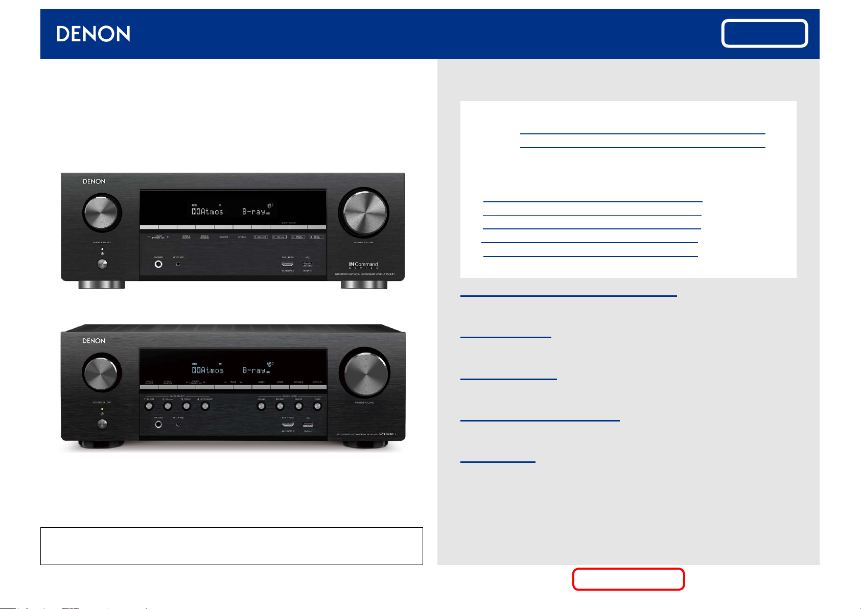
AVR-X1500H
AVR-S740H
Click here!
On-line service parts list
AVR-X1500H: http://dmedia.dmglobal.com/Document/DocumentDetails/24432
AVR-S740H: http://dmedia.dmglobal.com/Document/DocumentDetails/24433
ONLINE PARTS LIST (P5)
WEB owner’s manual
NA: http://manuals.denon.com/AVRX1500H/NA/EN/index.php
EU: http://manuals.denon.com/AVRX1500H/EU/EN/index.php
AP: http://manuals.denon.com/AVRX1500H/AP/ZH/index.php
JP: http://manuals.denon.com/AVRX1500H/JP/JA/index.php
NA: http://manuals.denon.com/AVRS740H/NA/EN/index.php
Upload is planned for the time of a future press release.
BEFORE SERVICING THIS UNIT
ELECTRICAL
MECHANICAL
•Forpurposesofimprovement,specicationsanddesignaresubjecttochangewithoutnotice.
• Please use this service manual whenreferringtotheoperatinginstructionswithoutfail.
• Some illustrations usedinthisservicemanualareslightlydifferentfromtheactualproduct.
REPAIR INFORMATION
UPDATING
Condential
Page 2

BEFORE SERVICING THIS UNIT
Before Servicing
SAFETY PRECAUTIONS
NOTE FOR SCHEMATIC DIAGRAM
HANDLING THE SEMICONDUCTOR AND OPTICS
ONLINE PARTS LIST
Accessing the Parts List
Searching Part Numbers or Ref. Numbers
NOTE FOR PARTS LIST
SERIAL NUMBER
Serial Number Organization
SKU Code of this Unit
POST-SERVICE PRECAUTIONS
This Unit
Electrical Mechanical Repair Information Updating
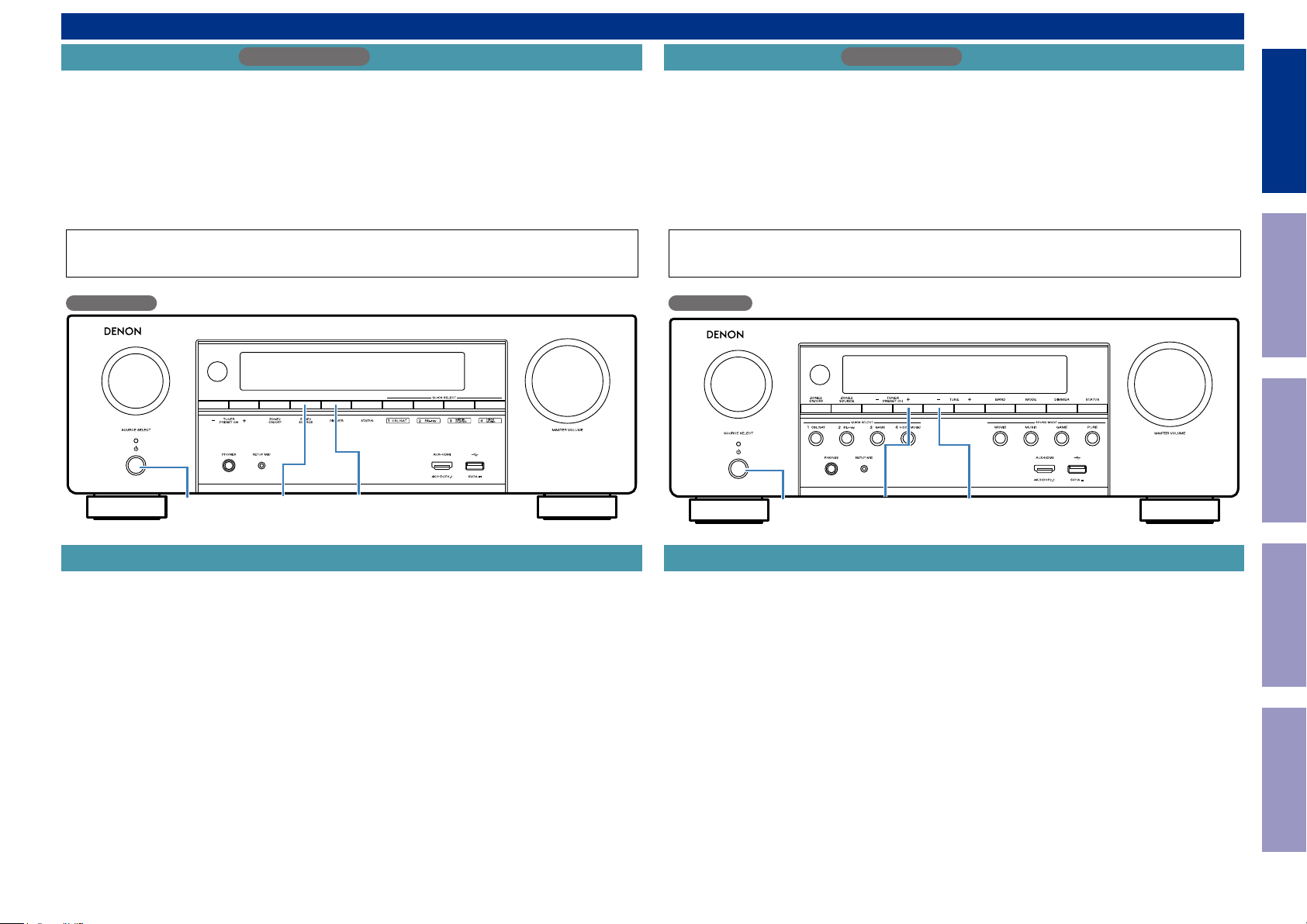
Initializing this Unit AVR-X1500H
JIG FOR SERVICING
Initializing this Unit AVR-S740H
JIG FOR SERVICING
2
Page 3

SAFETY PRECAUTIONS
The following items should be checked for continued protection of the customer and the service technician.
Leakage current check
Before returning the set to the customer, be sure to carry out either (1) a leakage current check or (2) a line to chassis resistance check. If the leakage current exceeds 0.5 milliamps, or if the resistance from chassis to either side of the power cord is less than 460 kohms, the set is defective.
Be sure to test for leakage current with the AC plug in both polarities, in addition, when the set's power is in each state (on, off and standby mode), if applicable.
Before Servicing
This Unit
CAUTION
Please heed the following cautions and instructions during servic-
ing and inspection.
◎ Heed the cautions!
Cautions which are delicate in particular for servicing are labeled on the cabinets, the parts and the
chassis, etc. Be sure to heed these cautions and the cautions described in the handling instructions.
◎ Cautions concerning electric shock!
(1) An AC voltage is impressed on this set, so if you touch internal metal parts when the set is energized,
you may get an electric shock. Avoid getting an electric shock, by using an isolating transformer and
wearing gloves when servicing while the set is energized, or by unplugging the power cord when
replacing parts, for example.
(2) There are high voltage parts inside. Handle with extra care when the set is energized.
◎ Caution concerning disassembly and assembly!
Through great care is taken when parts were manufactured from sheet metal, there may be burrs on the
edges of parts. The burrs could cause injury if ngers are moved across them in some rare cases. Wear
gloves to protect your hands.
◎ Use only designated parts!
The set's parts have specic safety properties (re resistance, voltage resistance, etc.). Be sure to use
parts which have the same properties for replacement. The burrs have the same properties. In particular,
for the important safety parts that are indicated by the z mark on schematic diagrams and parts lists,
be sure to use the designated parts.
◎ Be sure to mount parts and arrange the wires as they were originally placed!
For safety seasons, some parts use tapes, tubes or other insulating materials, and some parts are mounted away from the surface of printed circuit boards. Care should also be taken with the positions of the
wires by arranging them and using clamps to keep them away from heating and high voltage parts, so
be sure to set everything back as it was originally placed.
◎ Make a safety check after servicing!
Check that all screws, parts and wires removed or disconnected when servicing have been put back
in their original positions, check that no serviced parts have deteriorated the area around. Then make
an insulation check on the external metal connectors and between the blades of the power plug. And
otherwise check that safety is ensured.
(Insulation check procedure)
Unplug the power cord from the power outlet, disconnect the antenna, plugs, etc., and on the power.
Using a 500V insulation resistance tester, check that the insulation resistance value between the inplug
and the externally exposed metal parts (antenna terminal, headphones terminal, input terminal, etc.) is
1M Ω or greater. If it is less, the set must be inspected and repaired.
CAUTION
Many of the electric and the structural parts used in the set have special safety properties. In most cases
these properties are difcult to distinguish by sight, and the use of replacement parts with higher ratings (rated power and withstand voltage) does not necessarily guarantee that safety performance will
be preserved. Parts with safety properties are indicated as shown below on the wiring diagrams and the
parts list in this service manual. Be sure to replace them with the parts which have the designated part
number.
(1) Schematic diagrams Indicated by the z mark.
(2) Parts lists Indicated by the z mark.
The use of parts other than the designated parts could cause electric shocks, res or other dangerous
situations.
Concerning important safety parts
Electrical Mechanical Repair Information Updating
3
Page 4
NOTE FOR SCHEMATIC DIAGRAM
WARNING:
Parts indicated by the z mark have critical characteristics. Use ONLY replacement parts recommended
by the manufacturer.
CAUTION:
Before returning the set to the customer, be sure to carry out either (1) a leakage current check or (2)
a line to chassis resistance check. If the leakage current exceeds 0.5 milliamps, or if the resistance from
chassis to either side of the power cord is less than 460 kohms, the set is defective.
WARNING:
DO NOT return the set to the customer unless the problem is identied and remedied.
Before Servicing
This Unit
NOTICE:
(1) ALL RESISTANCE VALUES IN OHM. k=1,000 OHM / M=1,000,000 OHM
(2) ALL CAPACITANCE VALUES ARE EXPRESSED IN MICRO FARAD, UNLESS OTHERWISE INDICATED. P
INDICATES MICRO-MICRO FARAD. N INDICATES NANO FARAD.
(3) EACH VOLTAGE AND CURRENT ARE MEASURED AT NO SIGNAL INPUT CONDITION.
(4) CIRCUIT AND PARTS ARE SUBJECT TO CHANGE WITHOUT PRIOR NOTICE.
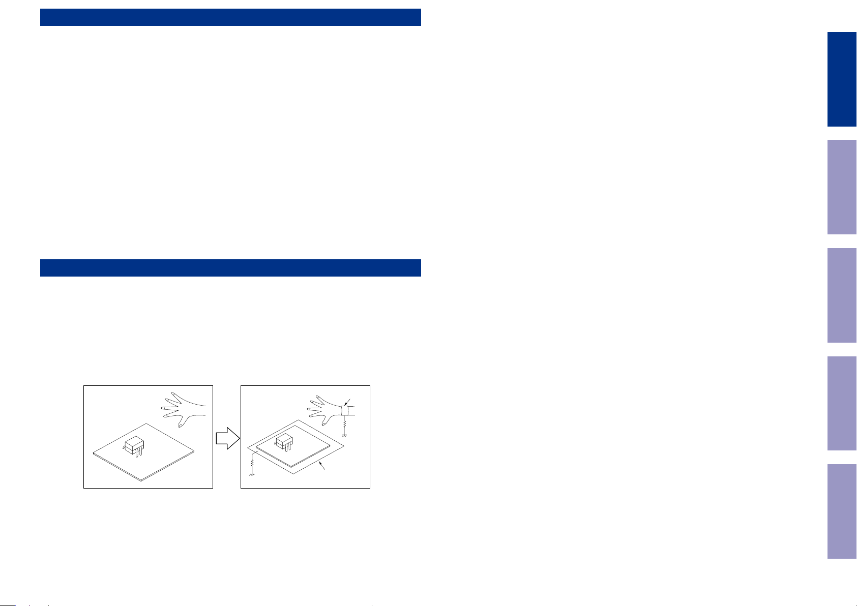
HANDLING THE SEMICONDUCTOR AND OPTICS
Electrostatic breakdown of the semi-conductors or optical pickup may occur due to a potential difference caused by electrostatic charge during unpacking or repair work.
1. Ground for Human Body
Be sure to wear a grounding band (1 M ohm) that is properly grounded to remove any static electricity
that may be charged on the body.
2. Ground for Workbench
Be sure to place a conductive sheet or copper plate with proper grounding (1 M ohm) on the workbench or other surface, where the semi-conductors are to be placed. Because the static electricity
charge on clothing will not escape through the body grounding band, be careful to avoid contacting
semi-conductors with your clothing
<Incorrect>
<Correct>
CBA
1MΩ
Grounding Band
CBA
Conductive Sheet or
Copper Plate
1MΩ
Electrical Mechanical Repair Information Updating
4
Page 5
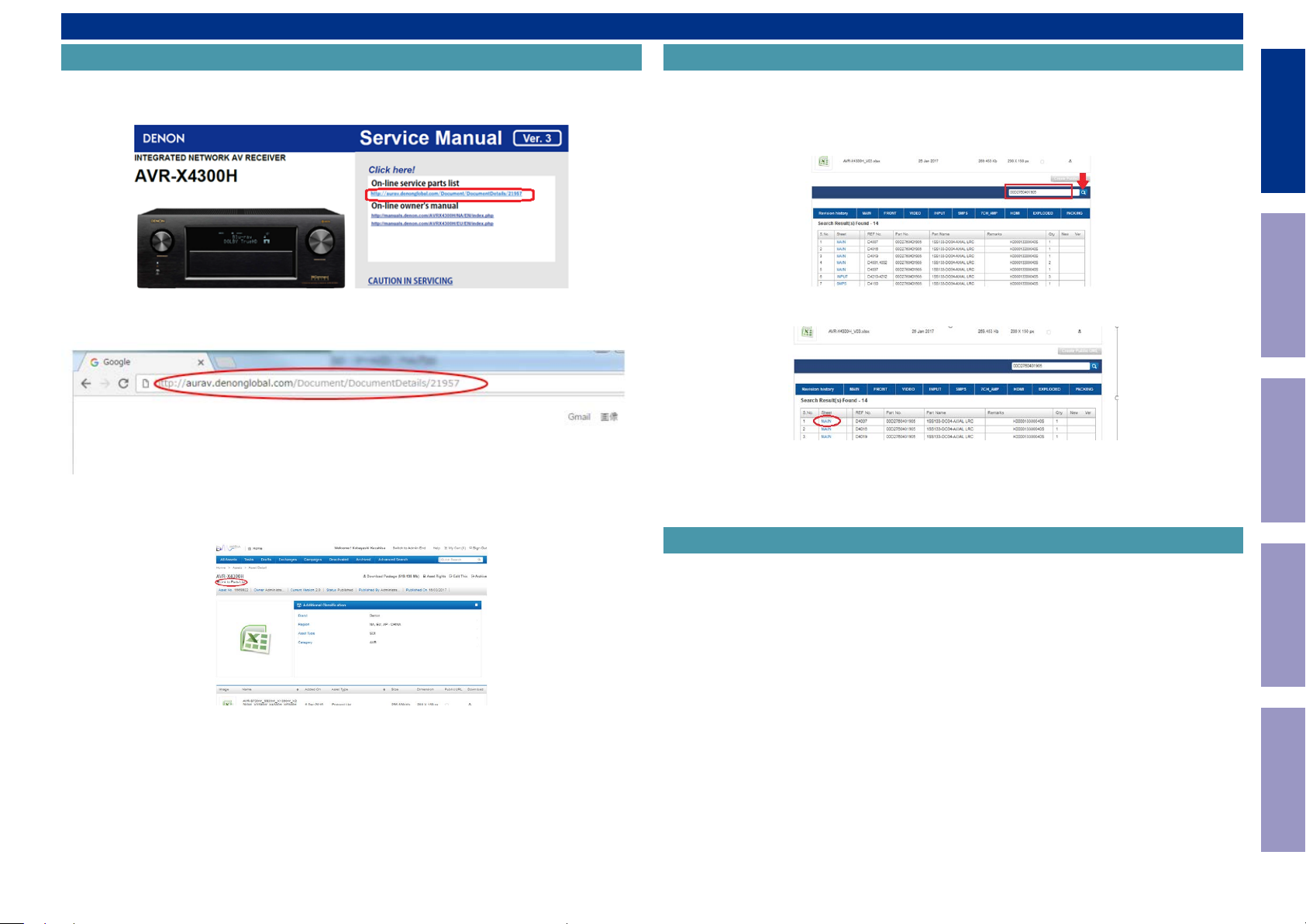
ONLINE PARTS LIST
Accessing the Parts List
(1) Access from the Service Manual
・ Click the URL link on the cover of the service manual.
Examples of display
Searching Part Numbers or Ref. Numbers
You can search a Parts List for part numbers or Ref. numbers.
(1) Enter the part number or Ref. number in the search window of the Parts List, and press the search
button.
(2) The search results are displayed.
The name of the sheet in which the search part is used and the part’s line are displayed.
Before Servicing
This Unit
Electrical Mechanical Repair Information Updating
NOTE : If the web browser does not open automatically, copy the URL and paste it into the address bar
of the web browser and then press Enter.
(2) Accessing the Part List from the Model Asset Screen.
・ Display Model Asset from New SDI.
・ Click the section displayed as ▼ Link to Part Lists under the model name.
NOTE : If the ▼ Link to Parts List section is not displayed, download the parts table from the Asset list.
(3) Next, click the "Sheet" section of the search results.
NOTE FOR PARTS LIST
1. Parts indicated by "
2. When ordering a part, make a clear distinction between "1" and "I" (i) to avoid mis-supplying.
3. A part ordered without specifying its part number can not be supplied.
4. Part indicated by "@" mark is not illustrated in the exploded and packaging view.
WARNING: Parts indicated by the z mark have critical characteristics. Use ONLY replacement parts
recommended by the manufacturer.
nsp
" on this table cannot be supplied.
5
Page 6
SERIAL NUMBER
Serial Number Organization
The 14-digit serial number that contains the code of the manufacturing plant and the manufacturing
date.
14 digits
Before Servicing
This Unit
SKU
code
Factory
code
The last
2digit of year
SKU Code of this Unit
Product SKU SKU Code
AVRX1500HBKE3
AVRX1500HBKE2
AVRX1500HBKE1C
AVRX1500HK
AVRS740HBKE3
Manufactured
Year, month
Month
(01 ~ 12)
Cumulative
serial number
AYW
AYX
AYY
AYZ
AYV
Electrical Mechanical Repair Information Updating
6
Page 7
POST-SERVICE PRECAUTIONS
Initializing this Unit
Make sure to initialize this unit after replacing the microcomputer or any peripheral equipment, or the
digital PCB.
AVR-X1500H
Initializing this Unit
Make sure to initialize this unit after replacing the microcomputer or any peripheral equipment, or the
digital PCB.
AVR-S740H
Before Servicing
This Unit
1. Press the power button to turn off the power.
2. While holding down buttons "ZONE2 SOURCE" and "DIMMER" simultaneously, press the power button to turn on the power.
3. Release the buttons after conrming that the display ashes at 1-second intervals.
* The unit is initialized.
Use network initialization mode to initialize the network related settings.
NOTE: • If the unit fails to enter the service mode in step 3, repeat the procedure from step 1.
• Initializing the device restores the customized settings to the factory settings. Write down
your settings in advance and recongure the settings after initialization.
AVR-X1500H
X
ZONE2
SOURCE
DIMMER
JIG FOR SERVICING
Use the following jigs (extension cable kit) when repairing the PCBs.
Order with your dealer for the jigs your dealer if necessary.
1. Press the power button to turn off the power.
2. While holding down buttons "TUNER PRESET CH +" and "TUNE -" simultaneously, press the power
button to turn on the power.
3. Release the buttons after conrming that the display ashes at 1-second intervals.
* The unit is initialized.
Use network initialization mode to initialize the network related settings.
NOTE: • If the unit fails to enter the service mode in step 3, repeat the procedure from step 1.
• Initializing the device restores the customized settings to the factory settings. Write down
your settings in advance and recongure the settings after initialization.
AVR-S740H
X
TUNER
PRESET CH +
TUNE -
JIG FOR SERVICING
Use the following jigs (extension cable kit) when repairing the PCBs.
Order with your dealer for the jigs your dealer if necessary.
Electrical Mechanical Repair Information Updating
8U-110084S : EXTENSION UNIT KIT : 1 Set
(See JIG FOR SERVICING)
8U-110084S : EXTENSION UNIT KIT : 1 Set
(See JIG FOR SERVICING)
7
Page 8
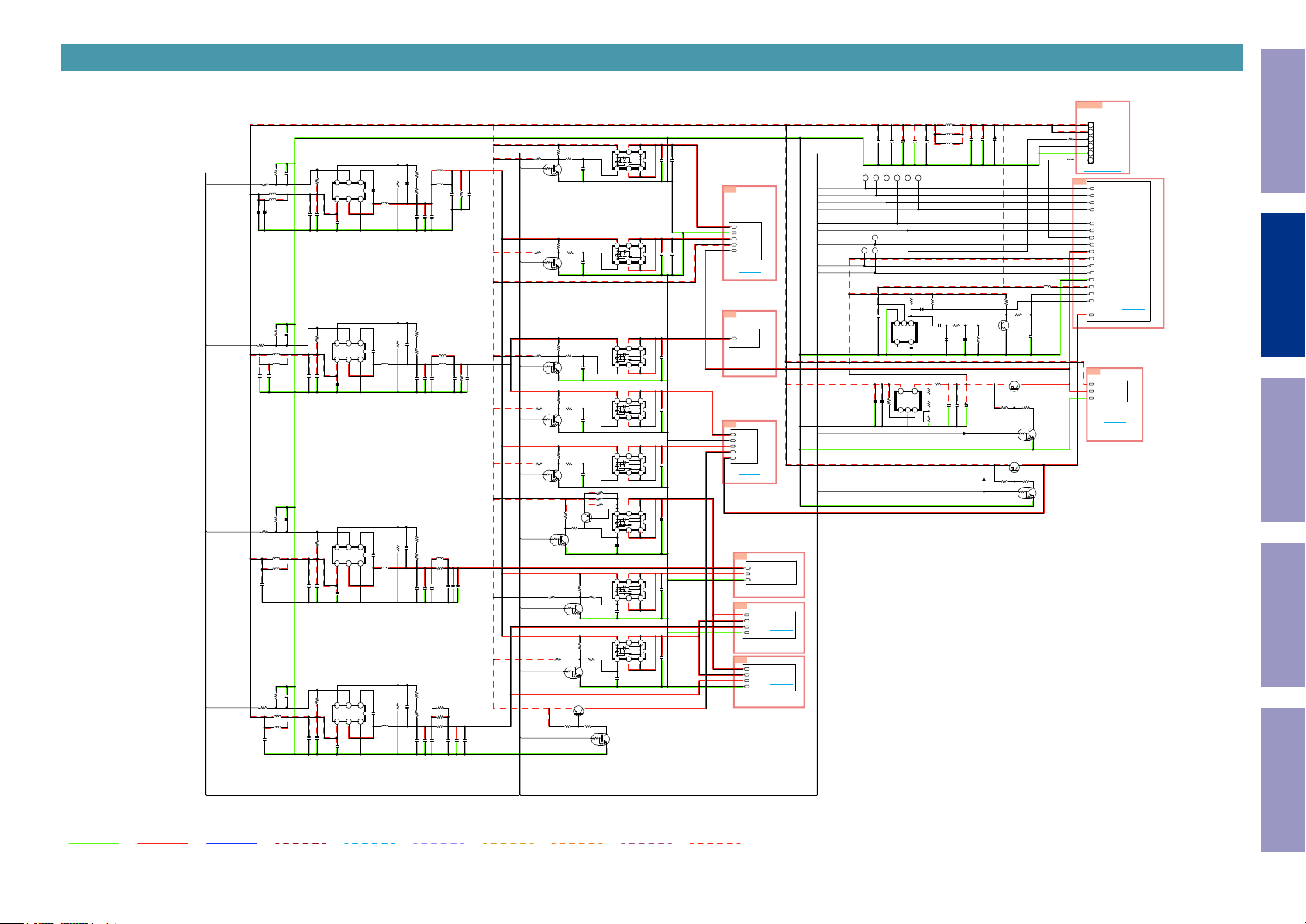
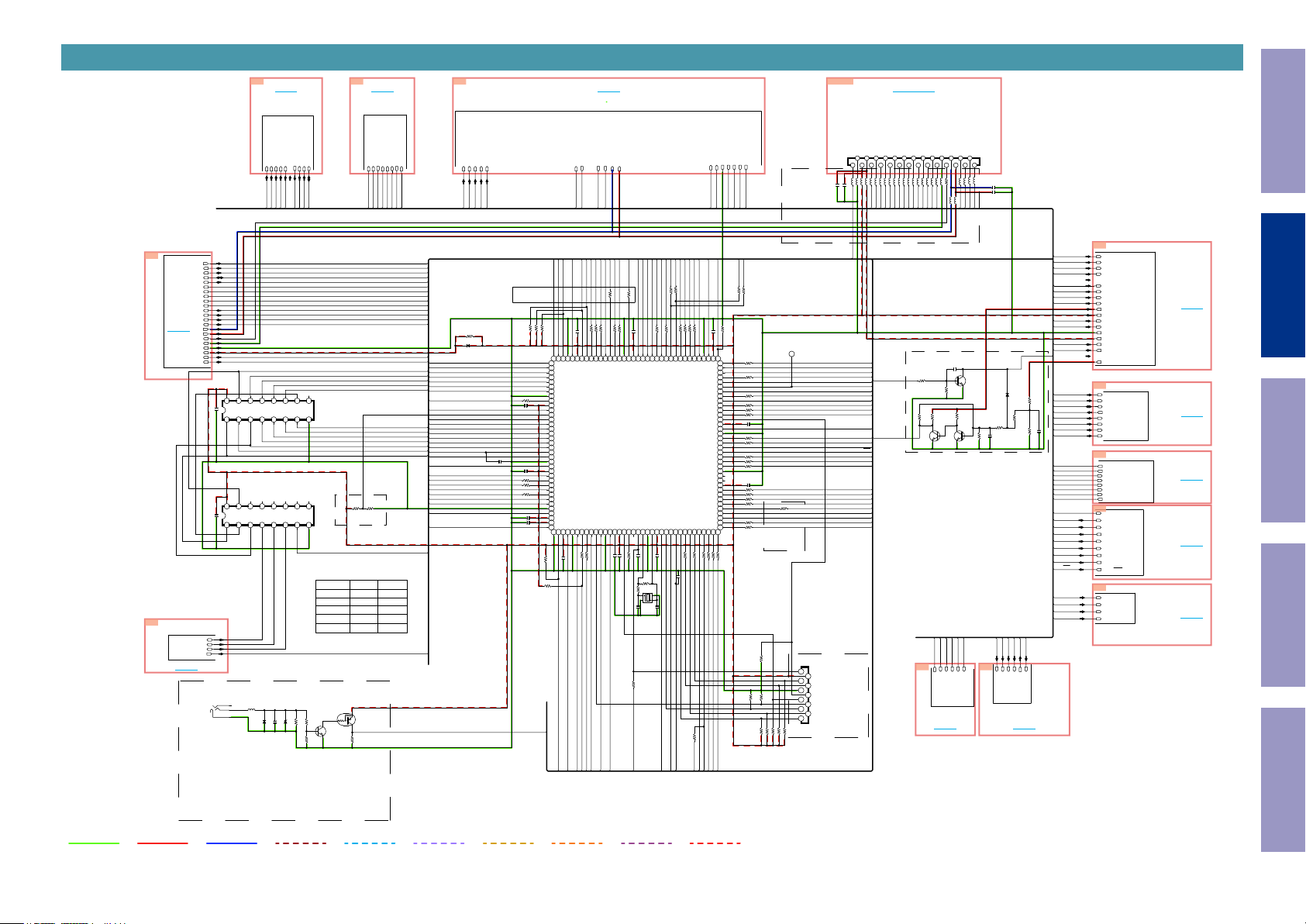
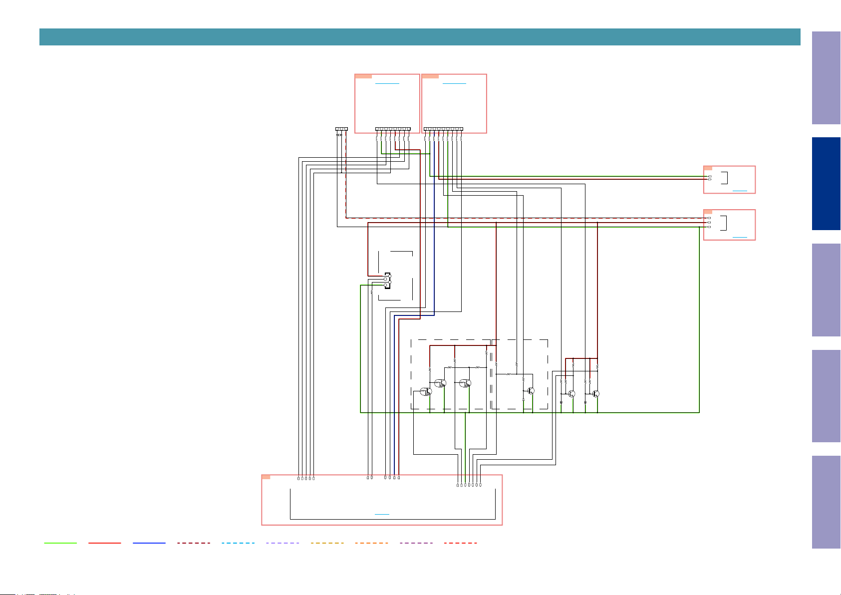
ELECTRICAL
Before Servicing
SCHEMATIC DIAGRAMS
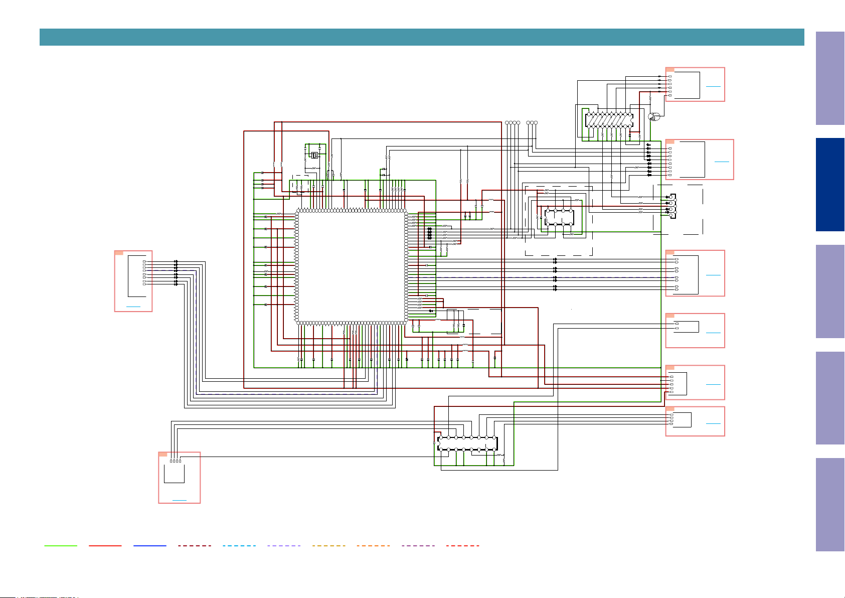
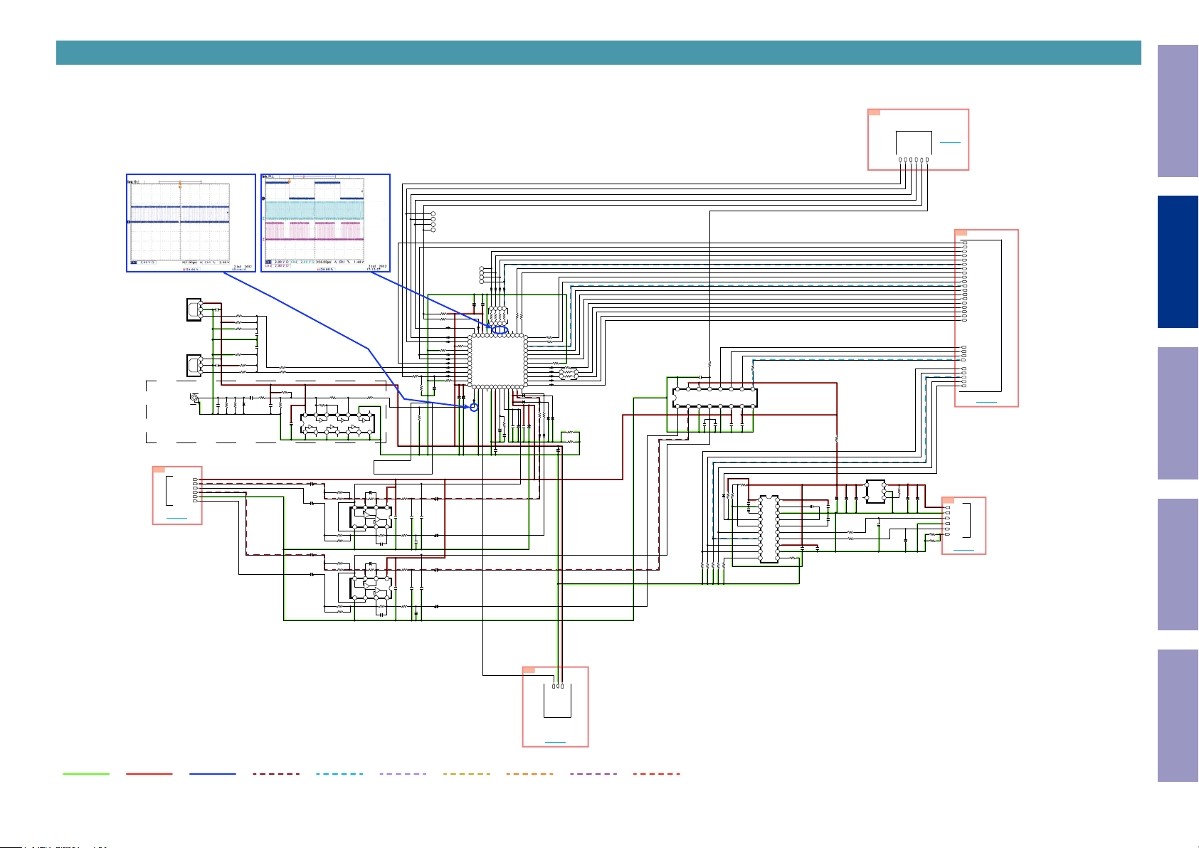
SCH01_HDMI_RX
SCH02_HDMI_TX
SCH03_OSD
SCH04_DIGITAL SUPPLY
SCH05_MCU
SCH06_MCU_LEVEL_CHG
SCH07_DIR
SCH08_PLD
SCH09_DSP
SCH10_MAIN DAC
SCH11_NETWORK
SCH12_ANALOG
SCH13_MAIN
SCH14_FRONT_HDMI
SCH15_DIFF-AMP
SCH16_PHONO & TUNER
SCH17_FRONT
SCH18_REGULATOR
SCH19_SMPS
LEVEL DIAGRAM
FRONT ch
CENTER, SURROUND ch
SURROUND BACK ch
SUBWOOFER ch
ZONE2 ch
BLOCK DIAGRAM
ANALOG AUDIO DIAGRAM
DIGITAL AUDIO DIAGRAM
VIDEO DIAGRAM
POWER DIAGRAM
WIRING DIAGRAM
SEMICONDUCTORS
This Unit
Electrical Mechanical Repair Information Updating
PRINTED CIRCUIT BOARDS
DIGITAL, F HDMI, TUNER, PHONE
MAIN
DIFF-AMP, BIAS-TR, PHONE WIRE GUIDE, HDMI CABLE GUIDE, SMPS, REGULATOR
FRONT, PHONE, USB WIRE GUIDE, STANDBY, MIC, USB
1. IC's
2. FL DISPLAY
3. Remote Code Table
8
Page 9
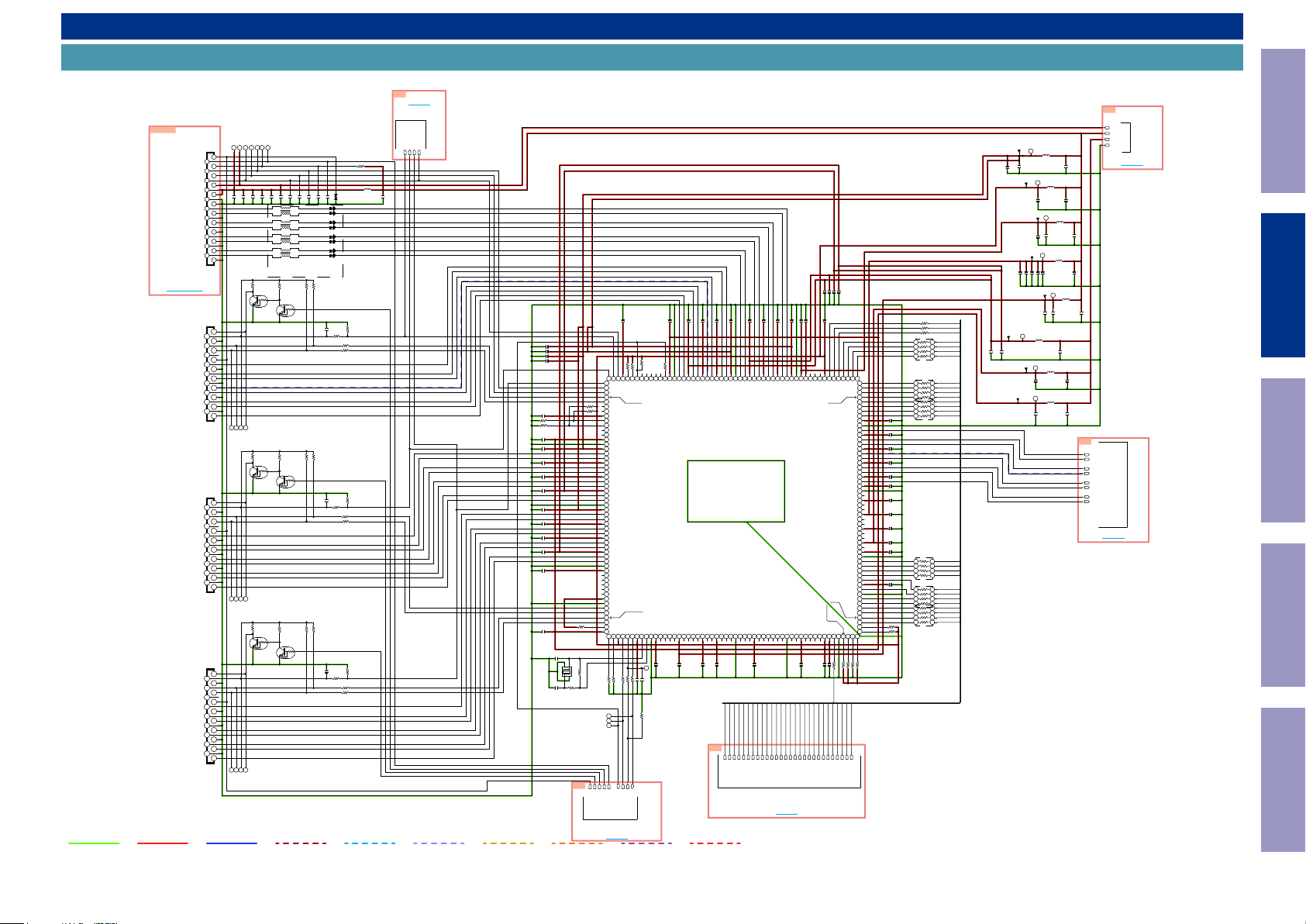
SCHEMATIC DIAGRAMS
PAR T
SCH01_HDMI_RX
H D MI_ RX PART
GND LINE
CN710
FROM A D 8195(F -H D MI IN )
04-6232-023-010-801+
TO CN811
19.HP DET
18.+5 V
17.GND
16.DDC D ATA
15.DDC C LK
14.NC
13.CEC
12.CK-
11.D1 SHIE LD
10.CK+
9.D 0-
8.D 1 SH IELD
7.D 0+
6.D 1-
5.D 2 SH IELD
4.D 1+
3.D 2-
2.D 2 SH IELD
CBL/S AT
1.D 2+
H DMI_IN PUT -1
19.HP DET
18.+5 V
17.GND
16.DDC D ATA
15.DDC C LK
14.NC
13.CEC
12.CK-
11.D1 SHIE LD
10.CK+
9.D 0-
D VD
8.D 1 SH IELD
7.D 0+
6.D 1-
5.D 2 SH IELD
4.D 1+
3.D 2-
2.D 2 SH IELD
H DMI_IN PUT -2
1.D 2+
19.HP DET
18.+5 V
17.GND
16.DDC D ATA
15.DDC C LK
14.NC
13.CEC
12.CK-
11.D1 SHIE LD
10.CK+
9.D 0-
8.D 1 SH IELD
7.D 0+
6.D 1-
Blu-ra y
5.D 2 SH IELD
4.D 1+
3.D 2-
2.D 2 SH IELD
H DMI_IN PUT -3
1.D 2+
POWER+ LINE
HPD _A
TXE N
DDCA_ SDA
DDCA_ SCL
RXA _5V
CEC5 V
CEC3 .3V
CEC3 .3V
DGND
DGND
RXA _CRXA _C+
DGND
RXA _0RXA _0+
DGND
RXA _1RXA _1+
DGND
RXA _2RXA _2+
DGND
CN710
CJP23GA 333ZR
1
CEC
2
3
4
5
6
7
8
9
10
11
12
13
14
1517
1618
19
20
22
23 21
JK701
CJJ9H021Z
19
18
17
16
15
14
13
12
11
10
9
8
7
6
5
4
3
2
1
JK711
CJJ9H021Z
19
18
17
16
15
14
13
12
11
10
9
8
7
6
5
4
3
2
1
JK721
CJJ9H021Z
19
18
17
16
15
14
13
12
11
10
9
8
7
6
5
4
3
2
1
POWER- LINE
TXEN
+5V_ F
CEC5 V
CEC3 V
CK_F
DA_F
HPD _F
0.1uF
1000P
1000P
1000P
1000P
C7101
CK_1
CK_2
CK_3
C7106
C7102
C7103
C7104
C7105
1
2 3
1
2 3
1
2 3
1
2 3
E3/ E1C/ K : 0 X 2
E2 : EXC 24CH900U
1k
10k
R7102
R7101
Q7101
HVT KRC102S
HVT KRC102S
PD_1
DA_1
+5V_ 1
H
1k
10k
R7112
R7111
Q7111
HVT KRC102S
HVT KRC102S
DA_2
+5V_ 2
HPD _2
1k
10k
R7121
R7122
Q7121
HVT KRC102S
HVT KRC102S
DA_3
+5V_ 3
HPD _3
ANALOG AUDIO DIGITAL AUDIO
Before Servicing
A0
TO 0A
TO OSD PAR T
AVDD33RX
HD MI1_H5 V
HD MI2_H5 V
HD MI3_H5 V
FRON T_H 5V
R7109 47k
L7101
D7131
CB03YT YH600
0.1uF
0.1uF
0.1uF
0.1uF
1000P
1000P
CVDC DS3 C05HD MI1
C7111
C7109
C7110
C7108
C7107
4
RN701
0 X 2
4
RN702
0 X 2
4
RN703
0 X 2
4
RN704
0 X 2
47k
47k
R7104
R7103
Q7102
0.1uF
C7113
R7106 0
R7107 0
R7108 0
47k
47k
R7114
R7113
Q7112
0.1uF
C7114
R7116 0
R7117 0
R7118 0
47k
47k
R7124
R7123
Q7122
0.1uF
C7115
R7126 0
R7127 0
R7128 0
0.1uF
C7112
OPEN
OPEN
OPEN
OPEN
C7167
C7165
C7168
0.1uF
0.1uF
0.1uF
0.1uF
0.1uF
0.1uF
0.1uF
0.1uF
47k
R7105
47k
R7115
47k
R7125
C7169
C7170
C7171
C7172
C7141
R7139 10k
R7140 OPEN
C7142
C7143
C7144
C7145
C7146
C7147
C7148
C7149
C7150
C7151
C7152
OPEN
OPEN
OPEN
OPEN
0.1uF
0.1uF
0.1uF
0.1uF
0.1uF
0.1uF
0.1uF
0.1uF
0.1uF
0.1uF
0.1uF
R7142 10k
0.1uF
C7153
50V/9p F
X7101
27MHz
C7154
R7143
50V/9p F
1k
C7140
R7138
106
108
107
109110111112113114115116117118119120121122123124125126127128129130131132133134135136137138139140141142143144145146147148149150151152153154155156157158159160161162
RX3P5 V
RX2P5 V
RX1P5 V
R7157
RX2SC L
10k
NIRQA 1
NIRQA 0
R7158
VDD33
OPEN
SCLK
MOSI
MISO
NCS
VDD11
VSS
AVDD33RX 1
P1RXC M
P1RXC P
AVDD11RX 1
P1RX0 M
P1RX0 P
AVDD11RX 1
P1RX1 M
P1RX1 P
AVDD11RX 1
P1RX2 M
P1RX2 P
VSS
AVDD33RX 0
P0RXC M
P0RXC P
AVDD11RX 0
P0RX0 M
P0RX0 P
AVDD11RX 0
P0RX1 M
P0RX1 P
AVDD11RX 0
P0RX2 M
P0RX2 P
VSS
VDD11
NOSD IRQ
CH1A SD0
CH1A LRCL K
CH1A BCLK
CH1A SPD IF
VDD33
VSS
RX1SD A
RX1SC L
NTEST
TX0A RCIN
TX1A RCIN
163
164
165
1M
R7144
R7146 47k
R7145 47k
R7147 47
P_DA
P_CK
787_HINT
C7139
C7138
C7137
C7136
C7135
10k
R7136
10k
10k
OPEN
R7137
R7135
94
95
96
97
98
99
104
100
101
103
105
102
VSS
HSCL 1
HSDA 1
VDD33
109.RX0P 5V
110.RX3S DA
111.RX3S CL
112.RX2S DA
P2RX2 P
VDD11
NIRQ1
NIRQ0
CH0A SD1
CH0A SD0
CH0A SD3
CH0A SD2
CH0A LRCL K
919293
P2RX2 M
AVDD11RX 2
88
89
90
P2RX1 P
P2RX0 P
P2RX1 M
AVDD11RX 2
83
84
858687
P2RXC P
P2RX0 M
P2RXC M
AVDD11RX 2
IC701
MN864787
159.RX0S DA
160.RX0S CL
161.CEC
162.VDD11
VDD11
Q21
Q20
Q19
Q18
VDD33
NC/X O
DEOU T
HSYN COU T
HSCL 0
HSDA 0
SYSC LK/X I
VSS
NRESE T
VSYN COUT
VDD33IO
166
R7148 1k
PCLK OUT
167
168
169
170
171
172
173
174
175
176
177
178
0.1uF
C7158
C7157
0.1uF
1000P
787_RST
C7156
R7149 47
C7155
10k
R7154
Q16
Q23
Q22
VDD11
Q17
VDD33IO
180
183
185
179
181
182
184
186
187
188
0.1uF
0.1uF
0.1uF
C7159
C7160
V
IDEO PLD_ POH I
VOUT _VS
VOUT _PC LK
0.1uF
C7134
C7133
C7132
71
727374
757677
78
798081
82
VSS
P3RX0 P
P3RX2 P
P3RX1 P
P3RX0 M
P3RX1 M
P3RX2 M
AVDD33RX 2
Q15
VSS
190
189
VOUT _PE
VOUT _HS
P3RXC P
AVDD11RX 3
AVDD11RX 3
AVDD11RX 3
Q7
Q6
Q14
Q13
Q12
Q11
Q10
Q9
Q8
VDD33IO
197
191
192
193
194
195
196
198
199
200
0.1uF
C7161
VOUT _D0 0
VOUT _D0 1
VOUT _D0 2
VOUT _D0 3
VOUT _D0 4
VOUT _D0 5
VOUT _D0 6
VOUT _D0 7
VOUT _D0 8
VOUT _D0 9
C7166
0.1uF
0.1uF
0.1uF
0.1uF
C7130
C7129
C7131
C7128
9
68
6
70
VSS
VDD11
PVDD33
P3RXC M
CH0A BCLK
AVDD33RX 3
Q5Q4Q3
Q2
VDD33IO
VSS
201
202
203
206
204
205
0.1uF
C7162
VOUT _D1 0
VOUT _D1 1
VOUT _D1 3
VOUT _D1 2
VOUT _D1 5
VOUT _D1 4
55
56
575859
60
61
62
6364656667
DEIN
VDD33
D23(R7 )
D21(R5 )
D22(R6 )
D20(R4 )
VSYN CIN
HSYN CIN
CH0AMC LK
CH0A SPD IF
D15(G7 )
54.D19(R3 )
D14(G6 )
53.D18(R2 )
D13(G5 )
52.D17(R1 )
51.D16(R0 )
D12(G4 )
VDD11
VSS
P0TX CM
AVDD11TX
P0TX CP
P0TX 0M
AVDD33TX
P0TX 0P
P0TX 1M
AVDD11TX
P0TX 1P
P0TX 2M
AVDD11TX
P0TX 2P
VDD11
VSS
P1TX CM
AVDD11TX
P1TX CP
P1TX 0M
AVDD33TX
P1TX 0P
P1TX 1M
AVDD11TX
P1TX 1P
P1TX 2M
AVDD11TX
P1TX 2P
VDD11
VSS
D11(G3 )
D10(G2 )
D9(G 1)
D8(G 0)
D7(B 7)
VDD11
4.D1 (B1)
10 11 1 2 13 1 4 15 1 6 17 1 8 19 2 0 21 2 2 23 2 4 25 2 6 27 2 8 29 30 3 1 32 3 3 34 3 5 36 3 7 38 3 9 40 4 1 42 4 3 44 4 5 46 4 7 48 4 9 50 5 1 52 5 3 54
D6(B 6)
3.D0 (B0)
VSS
2.TX 0HP D
D5(B 5)
1.TX 0SDA
D4(B 4)
D3(B 3)
D2(B 2)
215.TX1H PD
214.TX1S DA
213.TX1S CL
216.TX0S CL
1 2 3 4 5 6 7 8 9
Q1
Q0
VDD11
VSS
PCLK IN
VDD33
211
216
213
207
210
212
215
214
209
208
C7163 0.1 uF
C7164 0.1 uF
R7151 10k
R7152 10k
R7153 10k
R7155 10k
R7150 0
VOUT _PC LK
UT_D 18
VOUT _D2 1
VOUT _D2 0
VOUT _D2 3
VOUT _D2 2
VOUT _D1 7
VOUT _D1 6
VOUT _D1 9
VO
R7134 0
VOUT _PE
R7133 0
VOUT _HS
R7132 0
VOUT _VS
VOUT _D0 7
1234
5678
VOUT _D0 6
VOUT _D0 5
VOUT _D0 4
RN716 0x4
RN715
0x4
VOUT _D0 3
VOUT _D0 2
VOUT _D0 1
VOUT _D0 0
1 2 3 4
5 6 7 8
VOUT _D1 5
VOUT _D1 4
VOUT _D1 3
VOUT _D1 2
1 2 3 4
5 6 7 8
C7127
RN713 0x4
0.1uF
C7126
0.1uF
C7125
0.1uF
C7124
0.1uF
C7123
0.1uF
C7122
0.1uF
C7121
0.1uF
C7120
0.1uF
C7119
0.1uF
C7118
0.1uF
C7117
RN714
0.1uF
0x4
VOUT _D1 1
VOUT _D1 0
VOUT _D0 9
VOUT _D0 8
1 2 3 4
C7116
0.1uF
R7131
R7156
5 6 7 8
RN712 0x4
VOUT _D2 3
1234
5678
VOUT _D2 2
VOUT _D2 1
VOUT _D2 0
VOUT _D1 9
5678
1234
18
VOUT _D
VOUT _D1 7
10k
10k
VOUT _D1 6
RN711
0x4
AVDD33RX
L7102
CLZB LM21PG 300SN1D
C7174
10/6.3V
C7175
10/6.3V
VDD33
VDD33
L7103
CB05YT YH 221
C7177
4.7/6 .3V
PVDD33
PVDD33
L7104
CB05YT YH 221
C7179
4.7/6 .3V
C7180 OP EN
AVDD33TX
AVDD33TX
L7105
CB05YT YH 221
OPEN
OPEN
OPEN
OPEN
C7182
4.7/6 .3V
C7186
C7185
C7184
C7183
VDD33IO
VDD33IO
CB05YT YH 221
OPEN
C7188
4.7/6 .3V
C7189
AVDD11RX
AVDD11RX
L7107
CLZB LM21PG 300SN1D
C7192
C7191
10/6.3V
10/6.3V
C7190
AVDD11TX
L7108
AVDD11TX
CB05YT YH 221
C7194
4.7/6 .3V
VDD11
L7109
VDD11
CB05YT YH 221
C7196
4.7/6 .3V
A1
CEC5 V
CEC3 V3
CEC1 V1
DGND
FRO M
DIG ITAL SUPPLY
OPEN
C7173
C7176
4.7/6 .3V
C7178
C7181
L7106
OPEN
C7193
C7195
4.7/6 .3V
TO 1A
4.7/6 .3V
4.7/6 .3V
C7187
4.7/6 .3V
V
4.7/6 .3
A2
TX0_C M
TX0_C P
TX0_0M
TX0_0P
TX0_1M
TX0_1P
TX0_2M
TX0_2P
TO HD MI_ TX
TO 2A
A4
D19
VOU T_D 22
VOU T_D 23
VOU T_D 20
VOU T_D 21
VOU T_D 18
VOU T_
VOU T_D 16
VOU T_D 17
VOU T_D 14
VOU T_D 15
VOU T_D 12
VOU T_D 13
VOU T_D 11
VOU T_D 10
VOU T_D 09
TMDS SIGNAL
ANALOG VIDEO
A3
CEC_ COM
FROM MCU PART
DIGITAL VIDEO
HPD 3
PD2
HPD 1
H
TO 3A
VOU T_PE
VOU T_VS
VOU T_H S
PSCL
PSD A
HPD 6
MN864787_RS T
MN864787_H INT
VOU T_PC LK
VOU T_D 08
VOU T_D 07
VOU T_D 06
VOU T_D 05
VOU T_D 04
VOU T_D 03
VOU T_D 02
VOU T_D 01
VOU T_D 00
FROM LEGO P ART
TO 4A
STBY POWERHDMI
This Unit
Electrical Mechanical Repair Information Updating
9
Page 10
SCH02_HDMI_TX
H D MI_T X PA RT
A5
FROM OS D
TO 5A
2A
TX0_C M
TX0_C P
TX0_0M
X0_0P
T
TX0_1M
TX0_1P
TX0_2M
TX0_2P
TO A2
FROM HD MI_R X
A6
HD MI4_H5 V
HD MI5_H5 V
TO 6A
FROM OS D
19.HP DET
18.+5 V
17.GND
16.DDC D ATA
15.DDC C LK
14.NC
13.CEC
12.CK-
11.D1 SHIE LD
10.CK+
9.D 0-
8.D 1 SH IELD
7.D 0+
6.D 1-
GAME
5.D 2 SH IELD
4.D 1+
3.D 2-
2.D 2 SH IELD
1.D 2+
H DMI_IN PUT -4
19.HP DET
18.+5 V
17.GND
16.DDC D ATA
15.DDC C LK
14.NC
13.CEC
12.CK-
11.D1 SHIE LD
10.CK+
9.D 0-
8.D 1 SH IELD
7.D 0+
Med ia P la yer
6.D 1-
5.D 2 SH IELD
4.D 1+
3.D 2-
2.D 2 SH IELD
1.D 2+
H DMI_IN PUT -5
Before Servicing
A7
CEC5 V
10/6.3V
JK751
1
3
5
7
9
11
13
15
17
19
AA
D7233
A8
A9
1.D 2+
2
2.D 2 SH IELD
3.D 2-
4
4.D 1+
5.D 2 SH IELD
6
6.D 1-
7.D 0+
8
8.D 1 SH IELD
9.D 0-
10
10.CK+
11.D1 SHIE LD
12
12.CK-
13.CEC
14
14.UTI L/HEAC +
15.DDC C LK
16
16.DDC D ATA
17.GND
18
18.+5 V
19.HP DET
OPEN
P1T XCM
P1T XCP
P1T X0M
P1T X0P
P1T X1M
P1T X1P
P1T X2M
P1T X2P
788_GUI_ WRIT E
NET 3.3V
OSD _SPI_ CLK
OSD _SPI_ CS
OSD _SPI_ MI
OSD _SPI_ MO
CEC3 V3
CEC1 V1
DGND
TO 7A
TO OSD PRA T
FROM
H DMI_O UT
TO 8A
LE GO
TO 9A
FRO M DIG ITAL SUPPL Y PA RT
VDD33_TX
C7283
AVDD11RX_T X
C7292
ASQ S12U020R2
D7231AAD7230
AA
R7258
R7257 1k8
R7256 1k8
L7201
CB05YT YH 221
C7278
C7277
4.7/6 .3V
4.7/6 .3V
L7202
CB05YT YH 221
C7280
C7279
4.7/6 .3V
4.7/6 .3V
L7203
OPEN
L7209
10/6.3V
C7282
10/6.3V
OPEN
C7285
10/6.3V
C7291
10/6.3V
CB05YT YH 221
L7204
CB05YT YH 221
C7287
CB05YT YH 221
C7289
L7207
OPEN
L7210
CB05YT YH 221
CB05YT YH 221
OPEN
C7294
L7205
CB05YT YH 221
4.7/6 .3V
L7206
4.7/6 .3V
L7208
OPEN
100/50V
C7281
C7295
C7284
10/6.3V
C7286
4.7/6 .3V
C7288
4.7/6 .3V
OPEN
C7290
C7293
OP EN
D7228AAD7227AAD7232
D7226AAD7225AAD7224AAD7223
D7221
D7229
D7222
AA
KDS160
D7235
R7259
R7275
C7274 1uF
C7275 1uF
F
51/
4k7
AA
CEC
ARC
51/F
R7260
1234
RN725 10x4
D7234 KDS 160
Q7221
HVT KRC102S
AA
AA
CJJ9H021Z
CK_O UT
DA_O UT
+5V_ OUT
HPD _OUT
C7276 0.1uF
5
678
AA
0
VDD33_TX
3 4
RN724
EXC24C H900U
T7238
RN722
1 2
0x2
1234
T7239
R7253 0
R7254 0
PVDD33_TX
AVDD33TX_T X
VDD33IO_TX
VDD11_TX
ESD suppre ssor
D7238
Z5.1V
C7273
1uF
10k
R7255
TX2 +
TX2 -
TX1 +
TX1 -
TX0 +
TX0 -
TXC +
TXC -
C7247 0.1uF
C7248 0.1uF
C7249 0.1uF
R7226 10k
R7225 10k
R7202
HVT KRC102
R7212
HVT KRC102S
4
10k
47k
47k
R720
R7203
10k
Q7202
S
10k
47k
R7213
Q7212
47k
0.1uF
R7205
C7201
R7206 0
R7207 0
R7208 0
47k
R7214
47k
0.1uF
R7215
C7211
R7216 0
R7217 0
R7218 0
R7219 10k
R7263 10k
R7262 10k
C7254 0. 1uF
C7255 0. 1uF
C7256 0. 1uF
C7257 0. 1uF
C7258 0. 1uF
C7259 0. 1uF
C7260 0. 1uF
C7261 0. 1uF
C7262 0. 1uF
R7243 10k
R7244 10k
R7245
R7220 10k
788_HINT
788_RST
737475767778798081828384858687888990919293949596979899
RX0P 5V
RX3S DA
RX3S CL
RX2S DA
RX2S CL
VDD11
AVDD33RX 1
P1RX CM
P1RX CP
AVDD11RX 1
P1RX 0M
P1RX 0P
AVDD11RX 1
P1RX 1M
P1RX 1P
AVDD11RX 1
P1RX 2M
P1RX 2P
VSS
AVDD33RX 0
P0RX CM
P0RX CP
AVDD11RX 0
P0RX 0M
P0RX 0P
AVDD11RX 0
P0RX 1M
100101102103104105106107108
P0RX 1P
AVDD11RX 0
P0RX 2M
P0RX 2P
10k
R7227
CEC
TX1A RCIN
109
110
R7228 10k
R7261
10k
47
R7246
1k
R7201
Q7201
HVT KRC102S
19
18
17
16
15
14
13
12
11
10
9
8
7
6
5
4
CJJ9H021Z
3
2
1
JK731
CK_4
DA_4
+5V_ 4
HPD _4
1k
R7211
Q7211
HVT KRC102S
19
18
17
16
15
14
13
12
11
10
9
8
7
6
5
4
CJJ9H021Z
3
2
1
JK741
CK_5
DA_5
+5V_ 5
HPD _5
707172
68
69
NIRQ1
104.VSS
105.RX1S DA
106.RX1S CL
107.RX0S DA
108.RX0S CL
VDD11
TX0A RCIN
NTES T
111
112
113
C7263 0. 1uF
C7264 1000P
VSS
VDD11
P2RX 2P
P2RX 2M
69.VDD33
71.RX2P 5V
72.RX1P 5V
70.RX3P 5V
HSD A0
HSCL 0
NRESE T
VDD33
114
115
116
117
C7265 0.1uF
R7229 47
R7230 1k
R7231 47
C7271
50V/9p F
C7246 0. 1uF
6364656667
5859606162
P2RX 1P
P2RX 0P
P2RX 0M
P2RX 1M
AVDD11RX 2
AVDD11RX 2
IC721
CV IMN 864788
NC/X O
VDD11
SYSC LK/X I
VSS
VSS
VDD11
118
119
121
120
123
122
C7267 0.1uF
C7266 0.1uF
R7250
OPEN
R7249
OPEN
10k
R7251
R7247
1M
X7201
1k
R7248
27MHz
50V/9p F
C7272
B0
PSCL
PSD A
HPD 4
HPD 5
CEC_ COM
MN864788_RS T
MN864788_H INT
MN864788_H AINT
FROM MC U P ART
TO 0B
C7245 0. 1uF
AVDD11RX 2
SCLK /LPSA1
124
R7266 33
P2RX CP
P2RX CM
VSS
MOSI/LP SA0
125
126
R7267 33
R7252
I2S0
I2S1
I2S2
I2S3
FS
64FS
MCK
B1
C7244 0. 1uF
5354555657
VSS
P3RX 2P
AVDD33RX 2
CH0AMC LK
MISO
NCS
127
128
129
C7268 0.1 uF
R7232 100
R7268 33
10k
RXM CK/D SDM CK
MN864788_H AINT
C7242 0. 1uF
C7241 0. 1uF
49
505152
464748
45
P3RX 1P
P3RX 0P
P3RX 0M
P3RX 1M
P3RX 2M
AVDD11RX 3
AVDD11RX 3
36.NIRQA 1
35.VDD11
34.VSS
33.P0TX CM
4.CH 1ALR CLK
3.CH 1ASD 0
2.TX 0HP D
1.TX 0SDA
CH0A BCL K
CH0A SD3
CH0A LRCL K
VDD33IO
CH0A SD2
CH0A SD1
CH0A SD0
130
131
132
134
135
133
136
.1uF
C7269 0
R7238 33
R7237 33
R7236 33
R7235 33
R7234 100
R7233 100 C7243 0. 1uF
RXI2 S0/D SD1
RXI2 S1/D SD2
RXI2 S2/D SD3
RXI2 S3/D SD4
RXL RCK/ DSD 5
RXB CK/D SDS CK
TO PLD PA RT
TO 1B
C7239 0.1uF
C7236 OPEN
C7238 0. 1uF
C7240 0.1uF
C7237 OPEN
10k
R7224
R7223
HAIN T
OPEN
44
42
43
P3RX CP
P3RX CM
AVDD11RX 3
VDD33
NC
VDD11
137
138
139
C7270 0.1 uF
TXB CK
TXI2 S0
TXL RCK
33
41
37
383940
R7222
VSS
AVDD33RX 3
AVDD11TX
AVDD33TX
AVDD11TX
AVDD11TX
AVDD11TX
AVDD33TX
AVDD11TX
AVDD11TX
CH1A BCL K
TX1S CL
VSS
140
141
R7264 10k
C7231 0.1uF
VDD33
PVDD33
NIRQA 0
C7230 0.1uF
P0TX CP
P0TX 0M
C7229 0.1uF
P0TX 0P
P0TX 1M
C7228 0.1uF
P0TX 1P
P0TX 2M
C7227 0.1uF
P0TX 2P
C7226 0.1uF
VDD11
VSS
P1TX CM
C7225 0.1uF
P1TX CP
P1TX 0M
C7224 0.1uF
P1TX 0P
P1TX 1M
C7223 0.1uF
P1TX 1P
10 11 12 13 14 15 16 17 18 19 2 0 21 22 23 24 25 26 27 2 8 29 30 31 32 33 34 35 3 6
P1TX 2M
C7222 0.1uF
P1TX 2P
C7221 0.1uF
VDD11
6 7 8 9
VSS
TX0S CL
TX1H PD
TX1S DA
1 2 3 4 5
142
143
144
10k
R7221 10k
R7265
R7271 10k
R7272 10k
R7273 10k
R7274 10k
8 7 6 5
VCC
IC723
CSDOWP
C7297 0. 1uF
CVIEN 25QH32B 104HIP2 B
SN74LV C244APW R
R7277
33
R7280 3 3
33
R7278
R7279
33
DI
CLK
HOL D
VSS
4321
R7270
OPEN
33
R7269
PVDD33_TX
AVDD33RX 3_TX
AVDD33RX 2_TX
AVDD33RX 1_TX
AVDD33RX 0_TX
AVDD33TX _TX
VDD33IO_T X
VDD11_TX
IC722
123456789
OE1
OE2
C7296
10
11 12 15 16 17 18 19 20141 3
33
R7281
1
3
5
7
CN721
CJP07GA 333ZR
MP :O PEN
AVDD33RX_T X
AVDD11RX 3_TX
AVDD11RX 2_TX
AVDD11RX 1_TX
AVDD11RX 0_TX
AVDD11TX _TX
RN721
1 2
3 4
0x2
RN723
1 2
3 4
0x2
0.1uF
R7282 10k
R7283 47k
D7236 K DS160
D7237 K DS160
Q7222
HVT KRA104S
SCK
2
GND
MOS I
4
VCC
/CS
6
MISO
GND
1.00mm FFC
FOR OSD UPD ATE
This Unit
Electrical Mechanical Repair Information Updating
GND LINE
POWER+ LINE
POWER- LINE
ANALOG AUDIO DIGITAL AUDIO
TMDS SIGNAL
ANALOG VIDEO
DIGITAL VIDEO
STBY POWERHDMI
10
Page 11
SCH03_OSD
OSD P ART
Before Servicing
This Unit
B2
OSD _SPI_ MO
OSD _SPI_ MI
OSD _SPI_ CS
OSD _SPI_ CLK
NET 3.3V
GUI_ WRIT E
4k7
R7357
Q7301
HVT KRC102S
123456789
OE1
OE2
IC734
SN74LV C244APW R
33
33
R7365
R7363
10k
R736633R7358
0.1uF
C7354
R7361
B3
ADV 7623_RST
HSC L
HSD A
ADV 7623_SPI_ MI
R7362
100
0
R7350 100
R7351 100
R7352 100
R7353 100
ADV 7623_SPI_ CLK
7623_ROM _HOL D
1
3
5
7
CN731
CJP07GA 333ZR
ADV 7623_SPI_ MO
ADV 7623_SPI_ CS
MP :O PEN
5A
6A
B4
D1V 8H
DGND
DV3 V3
DV5 V
SWM 5V
B5
HINS ELA
HINS ELB
HINS ELC
H5V _DE T
CLK
WP
R7343 OP EN
10
11 12 15 16 17 18 19 201413
R7344
OPEN
5678
DI
IC732
VSS
CVIEN 25QH32B 104HIP2 B
+1 V8H 2
5P
332.4mA
<PV DD_1V8>
<DV DD_1V8>
L7308
L7307
CB03YT YH 600
V
C7338 10/ 6.3
C7340 0.1uF
C7341 10/6.3 V
C7342 0.1uF
R7333
10k
C7343 0. 1uF
C7344
0.1uF
C7345
8A
P1T XCM
P1T XCP
P1T X
0M
P1T X0P
P1T X1M
P1T X1P
P1T X2M
P1T X2P
FROM HD MI_T X
TO A8
0.1uF
C7346
0.1uF
R7335
10k
C7347
0.1uF
C7348
0.1uF
C7349
0.1uF
5P
36.7m A
C7351
C7350
1k
R7326
0
X7301
28.6363MHz
R7330
10k
R7329
CB03YT YH 600
500 ohm
R7332
109
110
111
112
113
114
115
116
117
118
119
120
121
122
123
124
125
126
127
128
129
130
131
132
133
134
135
136
137
138
139
140
141
142
143
144
R7327
1M
0.1uF
OPEN
C7335
R7328
0.1uF
0.1uF
1k/F
C7336
1k/F
C7337
R7331
DDCA_S DA
HP_C TRLA
5V_D ETA
PGND
RTERM
DDCA_S CL
CVDD
CGND
RXA_ CRXA_ C+
TVD D
RXA_0RXA_0+
CGND
RXA_1RXA_1+
TVD D
RXA_2RXA_2+
HP_C TRLB
5V_D ETB
DGND
DVD D
DDCB_S DA
DDCB_S CL
CVDD
CGND
RXB_ CRXB_ C+
TVD D
RXB_0RXB_0+
CGND
RXB_1RXB_1+
TVD D
RXB_2RXB_2+
HP_C TRLC
5V_D ETC
DDCC_SDA
1 2 3 4 5 6 7 8 9
CVDD
CGND
RXC_ C-
RXC_ C+
DDCC_SCL
C7301 0. 1uF
R7301 10k
0.1uF
C7334
100101102103104105106107108
PVDD
PGND
PVDD
XTAL
XTAL 1
RESET B
PWRD NB
AP5_OU T
SCLK _OUT
MCLK _OUT
AD V7623
RXC_0+
HP_C TRLD
TVD D
RXC_2-
RXC_0-
CGND
RXC_1-
RXC_1+
TVD D
RXC_2+
10 11 12 13 14 15 16 17 1 8 19 2 0 21 22 23 24 25 26 27 28 29 30 31 32 33 34 3 5 36
R7334
0.1uF
C7303
C7302 0. 1uF
10k
R7356
DGND
DVD D
IC731
5V_D ETD
DGND
4k7
C7333
0.1uF
AP0_OU T
AP1_OU T
AP2_OU T
AP3_OU T
AP4_OU T
DDCD_S CL
DVD D
DDCD_S DA
CVDD
CGND
R7359 10k
R7360 10k
C7305 0. 1uF
C7304 0.1uF
100
100
R7323
R7324
C7331
OPEN
C7330
OPEN
R7319 10k
R7322 10k
R7321 10k
R7320 10k
0.1uF
0.1uF
DVD D
CGND
SCL
DGND
SDAT A
AP0_IN
TXDDC_ SCL
TXDDC_ SDA
EXT_ SWIN G
RXD_1+
RXD_2-
TVD D
RXD_1-
0.1uF
C7307
C7329
AP1_IN
DVDDIO
AP2_IN
AP3_IN
7374757677787 98081828384
72
DGNDIO
R7318 10k
71
AP4_IN
R7317 10k
70
AP5_IN
R7316
69
SCLK _IN
R7315 10k
68
MCLK _IN
67
EP_M ISO
66
EP_M OSI
65
EP_C S
64
EP_SC K
63
CSB
62
ALSB
61
DVD D
60
DGND
59
CEC
58
TXGND
57
TX2+
56
TX2-
55
TXAV DD
54
TX1+
53
TX1-
52
TXGND
51
TX0+
50
TX0-
49
TXGND
48
TXC+
47
TXC-
46
TXGND
45
TXAV DD
R7341
44
R7340 1k8
43
R7305 10k
42
ARC+
R7304 10k
41
HP_A RC-
40
TXPL GND
39
TXPGND
38
TXPL VDD
37
RXD_2+
CVDD
0.1uF
C7318
CGND
TXPV DD
<TXP VDD_1V8 >
5.2m A
<TV DD_3V3>
292.2m A
<CV DD_1V8>
503.6m A
0.1uF
C7308
C7309
100/10V
CVIS N74CBT 3251PWR
10k
C7323 0.1uF
C7322 0.1uF
1k8
1uF
C7319
C7310
IC733
C7324
0.1uF
0.1uF
C7311
CB03YT YH 600
24.8m A
10/6.3V
C7353
C7332
8586878889909 1929394959697989 9
INT
INT2
INT_T X
DVDDIO
DGNDDIO
RXD_ C-
TVD D
RXD_0+
RXD_ C+
RXD_0-
0.1uF
C7306
4k7
R7349
R7348
R7313
0.1uF
C7325
OPEN
R7312 33
R7311 33
R7310 33
R7309
OPEN
R7308
47k
47k
OPEN
R7307
R7306
Place R7212 & R7213 & C7217
as cl ose a s po ssible
L7304
2K/F
1k6/ F
C7321
R7303
R7302
L7303
CB03YT YH 600
L7302
CB03YT YH 600
L7301
CB03YT YH600
0.1uF
0.1uF
C7315
C7313
C7312
C7314
10/6.3V
10/6.3V
16 15 14 13 1 2 11 10
B7B6B5
VCC
0.1uF
B3B4B2B1ANCOE
4k7
<D VDDIO_3V3 >
0.1uF
C7327
C7326
10/6.3V
to pi n40 on t he b ot of PCB
Reco mmend ed
: 887 oh m(1 %)
about 888.8 oh m
OPEN
OPEN
C7316
B8
0A
HD MI1_H5 V
HD MI2_H5 V
HD MI3_H5 V
FRON T_H 5V
FROM HD MI_R X
TO A0
1.5m A
L7306
CB03YT YH 600
C7328
10/6.3V
L7305
CB03YT YH 600
<TX AVDD_1V 8>
15mA
R7314 33
+1 V8H 1
OSD_ MI
OSD_ MO
OSD_ CS
OSD_ CLK
A_RS T
A_DA
A_CK
R7346 OPEN
R7345 10k
VCC
HOL D
CS
MO
CS
CLK
MI
R7364
0
+1 V8H 2
DO
1 2 3 4
C7352 0. 1uF
R7342 10k
OS D FLA SH PA RT
E3/ E1C/ K : E N25QH32B 104HIP 2B
E2 : EN25QH 64A104H IP
TX2 +
TX2 -
TX1 +
TX1 TX0 +
TX0 -
TXC +
TXC -
DV 3V3
OPEN
C7317
DV 5V
9
S2S1S0
GND
87654321
R7354
2k2
8k2
R7355
SCK
2
GND
MOS I
4
VCC
/CS
6
MISO
GND
TX2 +
TX2 -
TX1 +
TX1 -
TX0 +
TX0 -
TXC +
TXC -
HD MI4_H5 V
HD MI5_H5 V
TO 2B
FRO M LE GO
TO 3B
Electrical Mechanical Repair Information Updating
FRO M/T O MCU
1.00mm FFC
FOR OSD UPD ATE
TO A5
TO HD MI_ TX
TO A6
TO HD MI_ TX
TO 4B
FRO M
DIG ITAL SUPPL Y
TO 5B
FROM MC U
GND LINE
POWER+ LINE
POWER- LINE
ANALOG AUDIO DIGITAL AUDIO
TMDS SIGNAL
ANALOG VIDEO
DIGITAL VIDEO
STBY POWERHDMI
11
Page 12
SCH04_DIGITAL SUPPLY
D IGITAL SUPPLY PART
D5V _POW ER
D5V
0.1uF
C7412
D5V _POW ER
DA_ POW ER2
CEC_ POW ER
R7421
33
C7425
R7431
C7438
R7441
R7411
33
L7411
CB03YT YH
L7412
OPEN
C7413
CB03YT YH 600
0.1uF
33
CB03YT YH 600
0.1uF
33
CB03YT YH 600
C7451
0.1uF
Before Servicing
This Unit
CN741
CN741
OPEN
L7451
CB03YT YH600
R7483
0
L7404
CB03YT YH 600
CJP06GA 01ZY
TO BN601
B9
C0
123456
1.D 5.2V
2.D 5.2V
3.M_ RESE T
4.D _GND
5.D _GND
6.MAIN_ POW ER
D5V _POW ER
NET 5V_P OWE R
NET 3V3_PO WER
CEC_ POW ER
CEC_ POW ER2
CPU _POW ER
MAIN_P OWER
DV_ POW ER
SWM 3.3V
MCU _3V3
DA_ POW ER2
DA_ POW ER
DGND
MCU +5V
M_RE SET
BDO WN
SWM 5V
D5V
SWM 3.3V
DGND
TO 0C
TO 9B
2.5 mm 5PIN WIRE
FROM SMPS B 'D
Electrical Mechanical Repair Information Updating
TO MCU PA RT
TO LEV EL CH G B 'D
L7401
CB03YT YH 600
L7402
CB03YT YH 600
L7403
OPEN
0.1uF
C7401
C7402
C7403
OPEN
0.1uF
OPEN
OPEN
C7406
C7408
D5V_ PW
N5V_ PW
DA_P W2 DA _PW
R7451
R7453
OPEN
D3 .3V
L7414
100k
R7412
C7411
0.1uF
600
16V/10uF
C7414 16V/10uF
VBST
VFB
EN
4 5 6
OPEN
R7413
IC741
0.1uF
TPS563200DDC R
C7417
123
L7413
VIN
SW
(5040) 3.6 uH
GND
C7415 16V/10uF
0.1uF
C7416
CB03YT YH 600
R7415
33k2/F
L7415
OPEN
0
R7416
C7418 OPENC7431 OPEN
R7414 10K/ F
0.1uF
C7422
C7423 OPEN
R7417 47kR7427 47k
C7421
C7419
C7420
6.3V/ 22uF
6.3V/ 22uF
6.3V/ 22uF
10k
NET5V _POW ER
Q7401
HVT KRC104S
R7454 1k
NET3 V3_POW ER
Q7403
HVT KRC102S
R7452
10k
C7463
0.022uF
R7457
OPEN
R7456
27k
0.01uF
C7466
3 2 1
3 2 1
654
C7464
0.1uF
Q7402
FDC608P Z
C7465 O PENC7468
B6
LEGO 5V
DGND
NET 3.3V
654
OPEN
C7467
0.1uF
Q7404
FDC608P Z
D5V
SWM 3.3V
TO 6B
D5V _POW ER
NET 5V_P OWE R
NET 3V3_PO WER
CEC_ POW ER
CEC_ POW ER2
CPU _POW ER
DV_ POW ER
DA_ POW ER2
TO NET WO RK P AR T
DA_ POW ER
M3.3 V
B7
100k
R7422
C7424
0.1uF
L7421
L7422
OPEN
C7426
16V/10uF
C7427 16V/10uF
100k
C7437
R7432
0.1uF
L7431
L7432
OPEN
C7439 16V/10uF
100k
R7442
C7450
0.1uF
L7441
L7442
OPEN
C7452 16V/10uF
VBST
VFB
EN
OPEN
R7423
4 5 6
IC742
TPS563200DDC R
123
VIN
SW
GND
0.1uF
C7428 16V/10uF
C7429
VBST
VFB
EN
4 5 6
OPEN
R7433
IC743
TPS563200DDC R
123
VIN
SW
GND
0.1uF
C7440 16V/10uF
C7441
3
VBST
VFB
EN
OPEN
R744
4 5 6
IC744
TPS563200DDC R
123
VIN
SW
GND
0.1uF
C7453 16V/10uF
C7454
C7430
(5040) 3.6 uH
C7442
(5040) 2.2 uH
C7455
(5040) 2.2 uH
R7425
13k7/F
D1 .8V
L7424
0
0.1uF
L7423
0.1uF
L7433
0.1uF
L7443
CB05YT YH 221
R7426
R7424 10K/ F
L7425
OPEN
C7434
C7432
C7433
6.3V/ 22uF
6.3V/ 22uF
6.3V/ 22uF
C7435 0.1uF
C7436 OPEN
D SP
R7435
3k09/F
D1 .0V
L7434
0
OPEN
R7434 10K/ F
R7436
C7443 OPEN
0
R7437
C7446
C7444
C7445
6.3V/ 22uF
6.3V/ 22uF
6.3V/ 22uF
C7447 0.1uF
C7448 OPEN
C7449 OPEN
H DMI
4k7/ F
R7445
CE C1V 1
R7449
0
0
R7448
R7446
R7444 10K/ F
C7456 OPEN
0
R7447
0
C7459
C7458
C7457
6.3V/ 22uF
6.3V/ 22uF
6.3V/ 22uF
C7461 OPEN
C7462 OPEN
C7460 0.1uF
R7458 10k
DA_ POW ER
HVT KRC104S
R7462 10k
DV_ POW ER
HVT KRC104S
R7465 10k
DV_ POW ER
HVT KRC104S
CEC_ POW ER
DA_ POW ER
CEC_ POW ER
DV_ POW ER
Q7405
Q7407
Q7409
Q7411
HVT KRC104S
R7474
2k
R7459
R7463
R7466
Q7414
HVT
R7477
2k
Q7416
HVT KRC102S
OPEN
R7460
10k
OPEN
R7464
10k
OPEN
R7467
10k
10k
R7468
R7469
10k
KRC102S
Q7418
CVTI SA1530AC 1
R7480
10k
C7469
C7471
C7473
R7475
R7478
R7481
Q7419
HVT KRC102S
OPEN
OPEN
3k3
0.1uF
0.1uF
0.1uF
R7470 2.7
R7471 2.7
R7473 2.7
Q7412
CVTI SA1530AC 1
R7476
18k
R7479
18k
3 2 1
3 2 1
3 2 1
3 2 1
0.1uF
C7475
3 2 1
0.1uF
C7477
3 2 1
0.1uF
C7479
654
C7470
0.1uF
Q7406
FDC608P Z
654
Q7408
C7472
0.1uF
FDC608P Z
654
C7474
0.1uF
Q7410
FDC608P Z
654
C7476
0.1uF
Q7413
FDC608P Z
654
C7478
0.1uF
Q7415
FDC608P Z
654
Q7417
FDC608P Z
C7480
0.1uF
D1. 8V
PL
TO 7B
4B
D1V 8H
DGND
DV3 V3
DV5 V
SWM 5V
TO B4
B8
1A
TO HD MI_ RX
7A
TO HD MI_ TX
TO PLD PA RT
TO OSD PAR T
DA1 .0V
DA3 V3
TO 8B
DGND
TO DSP PA RT
CEC5 V
CEC3 V3
CEC1 V1
TO A1
DGND
CEC5 V
CEC3 V3
CEC1 V1
TO A7
DGND
CPU _POW ER
CEC_ POW ER2
C7481
OPEN
C7486
C7404
C7405
C7407
N3V3_P W
DV_P W
OPEN
R7494
C7487 1uF
CEC_ PW2
3
GNDCDOUT
NC
4
IC747
AP7361-Y -13
IN
1k
ADJ/NC
3
CB03YT YH 600
470/16V
CEC_ PW
CPU_ PW
k
10k
10
R7484
D7401
R7485
KDS160
R7486
2
C7483
VDD
1uF
OPEN
IC746
5 1
D7402
KDS160
OPEN
C7482
M3.3 V
R7498
0
47k
R7495
OUT
0
EN
GND
R7496
1 542
C7488 10/ 6.3V
15k
R7497
470/16V
100k
R7488
R7489
Q7420
100
CVT2 SC3052
4k7
0.1uF
C7484
R7487
C7489 OPEN
C7490 OPEN
D7403
KDS160
C7485
47k
Q7421
CVTIS A1530AC 1
SWM 3.3V
R7491
R7490
3k3
10k
Q7422
HVT KRC102S
Q7423
CVTIS A1530AC 1
R7493
R7492
D7404
3k3
10k
KDS160
Q7424
HVT KRC102S
GND LINE
POWER+ LINE
POWER- LINE
ANALOG AUDIO DIGITAL AUDIO
TMDS SIGNAL
ANALOG VIDEO
DIGITAL VIDEO
STBY POWERHDMI
12
Page 13
SCH05_MCU
C2
TO AUD IO PA RT
5B
TU_ INT
TU_ RST
TU_ SEN
TU_ SDIO
TU_ SCLK
ZVO L_DA TA
ZVO L_CL K
SEL_ CLK
SEL_ DAT A
MVO L_MU TE
MVO L_CL K
MVO L_DA TA
VINA
VINB
TO 2C
-12V
+12V
MIC_ SIGNAL
MIC_ GND
D
GND
MUT E_3V3
ZONE 2_MUT E
PRE_ MUT E
HINS ELA
HINS ELB
HINS ELC
H5V _DE T
TO OSD PART
TO B5
CJJ2D048Z D
RE MO TE IN
RE MO TE IN
AV RX1500H E 3 ON LY
3A
TO H D MI_R X
CEC_ COM
CEC_ COM
HPD 3
OE
QP4
QP5
VCC
0.1uF
QP0
STR
C7518
CP
D
1 2 3 4 5 6 7 8
OE
QP4
QP5
VCC
QP0
STR
0.1uF
CP
D
C7519
1 2 3 4 5 6 7 8
L9001
3
CB03YT YH 600
2
1
JK901
D9001
KDS160
TO A3
PSCL
PSD A
HPD 1
HPD 6
MN864787_RS T
MN864787_H INT
HPD 2
HPD 3
HPD 1
MN864787_RST
MN864787_HI NT
PSCL
PSDA
HPD 6
HPD 2
10111213141516
9
P6
QS1
QS2
QP7
Q
QP2
QP1
IC752
GND
QP3
CVIMC 74HC4094A DR2G
9
10111213141516
QS1
QS2
QP6
QP7
QP2
QP1
IC753
GND
QP3
CVIMC 74HC4094A DR2G
* A VRS740H /X1500H VER SION OPTIO N
VER.
X1500 E3
X1500 E2
X1500 E1 C
X1500 JP
S740H E 3
HVT KRA102S
3k3
OPEN
C9001
R90041kR9005
D9002
1000pF
Q9001
2k2
CVT2 SC3052
R9006
0B
TO H D MI_T X
HPD 5
HPD 5
R7581
R7582
OPTIO N
OPTIO N
VERS ION O PTIO N
R7581(PU )
OPEN
0
10K
10K
18K
Q9002
100k
R9007
TO B0
MN864788_H INT
HPD 4
PSCL
MN864788_HI NT
HPD 4
3K3
PSCL
MN864788_RST
R7582(PD )
0
OPEN
10K
22K
Before Servicing
C1
TO 1C
TO M CU L EV EL C HG.
CN751
TO BN12B1
TO FRON T B' D
1.25mm 27PIN FFC
This Unit
MCU PART
16.RED _LED
21.FL_ CLK
26.DGND
23.CPU _POW ER
17.WH /GRN _LED
18.RC_ IN
19.FL_ RST
20.FL_ CE
22.FL_ DAT A
24.MCU +5V
25.MCU _3V3
27.RES TORING_ FW
1.RE SET
2.MC U_3V3
3.TD O/T XD
4.TD I/RX D
5.D GND
6.UB
7.MD
8.EM LE
9.TR ST#
10.TCK
11.TMS
27
L7501
C7525 0.01uF
C7526 0.01uF
NET_ FACT _RST
ADV7623_S PI_C S
CEC_ POW ER2
DA_P OWE R
SEL_D ATA
DSP_ FLAG 3_C
DSP_ MISO
DSP_ MOSI
ADV7623_R ST
ADV7623_S PI_M O
ADV7623_S PI_C LK
ADV7623_S PI_M I
VEXP _DA TA
VEXP _STB
ZONE 2_MUTE
NET5 V_PO WER
7623_ROM_ HOL D
NET_ FACT _RST
E_TX D_M OEI
MP : O PE N
26 20
25 19
L7504
L7502
L7503
DSP_ RST
DSP_ ICS
DSP_ CLK
HSD A
HSCL
DSP_ BSY
TU_S CLK
TU_S DIO
TU_S EN
VEXP _CLK
VEXP _OE
1.00mm FFC
E20/ EMU LAT OR
CURRE NT_D ET
AMPSIG _DET
-12V
MN864788_H AINT
CEC_ COM
PSD A
MN864788_RS T
CEC_ COM
MN864788_HA INT
PSDA
TU_IN T
TU_R ST
TU_S EN
TU_S DIO
TU_S CLK
ZVOL _DA TA
ZVOL _CLK
SEL_C LK
SEL_D ATA
MVOL _MUT E
MVOL _CLK
MVOL _DA TA
VINA
VINB
ZONE 2_MUTE
PRE_M UTE
VEXP _OE
HPD 5
H
PD6
VINA
VINB
HPD 4
HPD 3
HPD 2
D1
HP
VEXP _CLK
VEXP _DA TA
VEXP _STB
ADC_ RST
H5V_ DET
CURREN T_D ET
THER MAL_B
NET3 V3_POW ER
D5V_ POW ER
CEC_ POW ER
DV_P OWE R
DIR_D OUT
DIR_D IN
H/P_ DET /MIC _DET
MN864787_RST
DIR_R ST
MN864788_HI NT
MN864787_HI NT
TU_IN T
CEC_ IN
THER MAL_A
TEMP _SEN SOR
DSP_ ROM_ WRIT E
MN864788_RST
FL_RS T
DIR_C E
DIR_C LK
AIOS4_S TBY _STA TUS
AIOS4_W AKE UP
CPU_ POW ER
MAIN_PO WER
MN864788_HA INT
CEC_ OUT
H/P _RLY
FRON T_RL Y
C/S_ RLY
SB_ RLY
HI-B _RLY
HI-B_ RLY
FRONT _RLY
C/S_ RLY
H/P_ RLY
SB_R LY
AVR -X1500H E 3
ONL Y USE
OTH ER O PEN
R7579
0
D7501
OPEN
R7551 33
C7514
C7527
OPEN
C7515
0.1uF
R7552 33
R7553 33
R7549 33
C7516 0. 1uF
C7517 0.1uF
B/PIR IN_D E
R7558 1k
0.1uF
R7560 1k
R7559 1k
AN0
PE1
R7501
R7508
10k
KEY_ 1
HI-B_ RLY
AMPSIG_ DET
DC_D ET/ ASO
AN1
109
PE5
AN2
VSS
110
111
PE0
112
P64
113
P63
114
P62
115
P61
116
VSS
117
P60
118
VCC
119
AN7
120
AN6
121
PD5
122
PD4
123
PD3
124
PD2
125
IRQ1
126
IRQ0
127
P93
128
P92
129
AN015
130
VSS
131
P90
132
VCC
133
AN007
134
AN006
135
AN005
136
AN004
137
AN003
138
AN002
13
9
AN001
140
VREFL 0
141
P40
142
VREFH 0
143
AVCC0
144
P03/IRQ 11
P07
1 2 3 4 5 6 7 8 9
AVSS0
VREFH
P05/IRQ 13
10k
C7501 0. 1uF
POWE R_KE Y
RED_ LED
TXD
P70
VREFL
+12V
RXD
TXD
AMPSIG_ DET
CURREN T_D ET
RXD
FL_CE
KEY_ 3
KEY_ 2
FL_CL K
FL_D ATA
0.1uF
C7513
R7547 3 3
R7546 3 3
R7548 3 3
100101102103104105106107108
VCC
P66
P65
IRQ7/ AN5
IRQ6/ AN4
TXD 6
P02
PF5
RXD6
EMLE
10 11 12 13 14 15 16 17 1 8 19 2 0 21 22 23 24 25 26 27 28 29 30 31 32 33 34 3 5 36
R7502 33
R7503 33
SB_R LY
RXD
W/G_ LED
VSEL_ A
TXD
H5V_ DET
ZVOL _CLK
MVOL _CLK
R900333R9002
R7545 3 3
P67
PA1
PA0
CVIR 5F5631FDDFB
PJ5
PJ3
VSS
VCL
C7502 0. 1uF
VSEL_ B
ISEL_ A
ISEL_ B
DAC_ MS
C/S_ RLY
DAC_ RST
APLD _CLK
PRE_M UTE
ZVOL _DA TA
MVOL _DA TA
DA_P OWE R2
33
R7539 33
0.1uF
7543 33
C7512
R7544 3 3
PA2
R7542 3 3
R
PB0
VCC
PA4
P72
P71
PA7
PA6
VSS
PA3
PA5
PB1
IC751
MD
XCOU T
XTAL
VCC
TRST #
XCIN
RESET
VSS
P35(IN)
VBAT T
EXTA L
0.1uF
R7504 10k
C7503 0. 1uF
C7504
C7507 0.1uF
R7505
1M
0
R7506
X7501
10MHz
C7505
50V/30pF
C7506
100
R7561
DSP_ FLAG 0
M_RES ET
RC_IN
APLD _DA TA
R7538 33
PB3
PB2
TIOC D0/I RQ3-D S
IRQ2-D S
C7508
50V/30pF
BDO WN
DGND
THE RMAL_A
THE RMAL_B
DC_ DET /ASO
H/P _DET /MIC _DE T
H/P _DET
MIC_ DET
L7501~ L7520
L7522~ L7527
DC_ DET /ASO
H/P_ DET /MIC _DET
H/P _DET
MIC_ DET
THE RMAL_A
PSCL
PSDA
PLDE RR
SEL_C LK
H/P_ RLY
APLD _CS
R7536 33
R7537 33
R7535 33
PB5
PB4
TCK
TMS
TDI/ RXD 1
R7509 33
0.1uF
DAC_ DAT A
FRONT _RLY
33
R7541
0.1uF
10k
R7533
C7511
R7534 33
VCC
PC1
7374757677787 9808182838485868 788899091929394959 6979899
R7531 33
P74
72
PC2
VSS
P73
PB7
PB6
71
P75
70
PC2
R7530 33
69
P76
68
P75
67
PC3
66
PC4
R7529 33
65
SCK1 0
64
RXD1 0
R7528 33
63
TXD 10
R7527 33
62
PC5
R7526 33
61
PC6
60
PC7
C7510 0.1uF
59
VCC
58
P83
57
VSS
R7525 33
56
TXD 2
R7524 10
55
SCK2
54
RXD2
53
P53
R7523 33
52
P54
R7522 33
51
P55
R7521 33
50
P56
49
VSS_US B
48
USB0_D P
47
USB0_D M
C7509 0.1uF
46
VCC_US B
R7520 33
45
P12
R7519 33
44
P13
R7518 33
43
P14
R7517 33
42
P15
41
P86
40
P16
39
P87
R7515 33
P17
38
R7514 33
37
TDO /TXD 1
P25
P24
P23
P22
TXD 0
RXD0
R7511 33
R7583 33
R7512 33
R7513 33
R7510 33
0
R7584
E_RT S_MO EI
MVOL _MUT E
E_CT S_MIE O
E_RX D_MI EO
VOLU ME_M UTE
TU_R ST
:CB 03YTY H600
THE RMAL_B
DAC_ CLK
R7540 33
T1
R9001 33
AVR -X1500H E 3
ONL Y USE
OTH ER O PEN
CN752
10k
CJP11GA 333ZR
R7499
1
2
3
4
5
6
4k7
R7562
7
10k
R7563
R7564 4k7
8
9
10
11
R7567 4k7
R7565 4k7
R7566 4k7
R7568 4k7
2224
18 16
2123
17 151413121110987654321
L7511
L7512
L7509
L7510
L7507
L7508
L7505
L7506
W/G_ LED
CPU_P OWE R
RC_IN
FL_CE
FL_RS T
FL_D ATA
FL_CL K
RED_ LED
CEC_ OUT
CEC_ IN
14.KEY _2
15.KEY _1
L7514
L7513
KEY_ 1
KEY_ 2
11.VSE L_A
9.B/ P_IRI N_DE
10.H/P _DE T
12.VSE L_B
13.KEY _3
L7516
L7517
L7518
L7515
L7519
VSEL_ B
B/PIR IN_D E
KEY_ 3
VSEL_ A
H/P_ DET
HD MI C EC_ PART
R7569
10k
4k7
2M2
R7572
R7571
Q7502
CVT2 SC3052
PLDE RR
C6
PLD ERR
TO 6C
6.-12V
7.MIC _SIGNA L
8.MIC _GND
5.+ 12V
0
L7524
L7520
R7580
L7523
L7522
C7520
OPEN
100k
R7570
R7573
Q7503
CVT2 SC3052
APLD _CS
APLD _CLK
APLD _DA TA
VOLU ME_M UTE
APLD _CS
APLD _CL K
APLD _D ATA
TO P LD
4.PO WER _KEY
3.MIC _DE T
2.ISE L_B
1.ISE L_A
CN751
C7524 0 .01uF
L7525
L7527
L7526
C7523 0 .01uF
ISEL_ B
ISEL_ A
MIC_D ET
POWE R_KE Y
9B
D5V_ POW ER
NET5 V_PO WER
NET3 V3_POW ER
CEC_ POW ER
CEC_ POW ER2
CPU_ POW ER
MAIN_PO WER
DV_P OWE R
DA_ POW ER2
DA_ POW ER
M_RE SET
BDO WN
CEC_ COM
Q7501
HVT KTC2875B
D7502
47k
R7575
220k
100k
220P
R7574
C7521
DIR_C E
DIR_C LK
DIR_R ST
MVOL _MUT E
C7
IR_R ST
DIR_ CE
D
MVO L_MU TE
VOL UME_ MUTE
TO D IR PART
ADV7623_RST
HSCL
KDS160
1k2
HSDA
R7577
ADV7623_SPI_ MI
ADV7623_SPI_ MO
27k
R7576
ADV7623_SPI_ CS
ADV7623_SPI_ CLK
7623_ROM_HO LD
C7522 0. 1uF
R7578 3k3
E_RX D_MI EO
E_CT S_MIE O
E_TX D_M OEI
E_RT S_MO EI
AIOS4_W AKE UP
AIOS4_S TBY _STA TUS
NET_ FACT _RST
TEMP _SEN SOR
DSP_ ROM_ WRIT E
DSP_ ICS
DSP_ MOSI
DSP_ MISO
DSP_ CLK
DSP_ RST
DSP_ FLAG 0
DSP_ FLAG 3_C
DSP_ BSY
DAC _RST
DAC _DA TA
DAC _CLK
DAC _MS
DIR_D IN
ADC_ RST
DIR_D OUT
DIR_ DIN
DIR_ CLK
ADC _RST
DIR_ DOU T
D5V _POW ER
NET 5V_P OWE R
NET 3V3_PO WER
CEC_ POW ER
CEC_ POW ER2
CPU _POW ER
MAIN_P OWER
DV_ POW E
SWM 3.3V
MCU _3V3
DA_ POW ER2
DA_ POW ER
DGND
MCU +5V
M_RE SET
BDO WN
SWM 5V
3B
ADV 7623_RST
HSC L
HSD A
ADV 7623_SPI_ MI
ADV 7623_SPI_ MO
ADV 7623_SPI_ CS
ADV 7623_SPI_ CLK
7623_ROM _HOL D
C3
E_RX D_M IEO
E_CT S_M IEO
E_T XD_ MOEI
E_RT S_M OEI
AIOS 4_WAK EUP
AIOS 4_STBY _ST ATU S
NET _FAC T_RS T
TEM P_SE NSOR
C4
DSP _ROM _WR ITE
DSP _ICS
DSP _MOS I
DSP _MISO
DSP _CLK
DSP _RST
DSP _FLA G0
DSP _FLA G3_C
DSP _BSY
C5
DAC _RST
DAC _DA TA
DAC _CLK
DAC _MS
R
TO B9
TO DIGIT A L SU PPLY
TO B3
TO OS D
TO 3C
TO L EG O
TO 4C
TO D S P P ART
TO 5C
TO MAIN D AC
Electrical Mechanical Repair Information Updating
TO 7C
GND LINE
POWER+ LINE
POWER- LINE
ANALOG AUDIO DIGITAL AUDIO
TMDS SIGNAL
ANALOG VIDEO
DIGITAL VIDEO
STBY POWERHDMI
13
Page 14
SCH06_MCU_LEVEL_CHG
Before Servicing
This Unit
MCU_LE V EL_CHG PART
CN756
CJP03G I288ZY
5.+12V
L7557
6.FRO NT_ RLY
L7558
CB03YT YH600
8.SB _RLY
7.C/ S_RLY
87654321
L7559
CB03YT YH 600
CB03YT YH 600
CN754
TO BN501
TO MAIN B 'D
2.0 mm 9PIN WAF ER
3.-12V
4.MU TE_+ B
5.AS O_DE T
1.CU RRENT_ DET
2.CU RRENT_ GND
1 2 3 4 5 6 7 8 9
L7560
CB03YT YH600
CB03YT YH 600
CB03YT YH 600
CB03YT YH 600
CB03YT YH 600
CB03YT YH 600
L7561
L7564
L7565
L7562
L7563
9.AMPSI G_DE T
8.TH ERMALD ET_ B
7.DC _PRO T
6.DGND
CN754
CJP09G I288ZY
CB03YT YH 600
CB03YT YH 600
CB03YT YH 600
L7566
L7567
L7568
C8
TO
RLY _GND
MUT E_+ B
ANA LOG
Electrical Mechanical Repair Information Updating
CN753
TO BN502
TO MAIN B 'D
2.0 mm 9PIN WAF ER
1.TH ERMALD ET_ A
3.H/ P_RL Y
2.RLY _GND
CN753
4.HI- B_RL Y
CB03YT YH 600
CB03YT YH 600
L7554CB 03YTY H600
L7553CB 03YTY H600
L7556CB 03YTY H600
L7552
L7551
1.DGND
2.HI- B_RL Y
3.D5 V
321
CJP08G I288ZY
C7594
0.1uF
TO 8C
0C
D5V
FRO M
SWM 3.3V
DIG ITAL
DGND
SUPPL Y
TO C0
CN755
CJP04G B113ZY
1
1.3. 3V
24
2.TX
3
3.RX
4.D GND
33
R7585
UPD ATE
1.00mm 4PIN FFC
RC102S
10k
R7590
R7589
3k3
3k9
10k
R7593
R7591
R7592
3k3
100
R7594
PR OT EC T P AR TS
Q7594
CVT2 SC3052
0.01uF
C7591
DC_ DET /ASO
22k
R7597
22k
R7600
100
100
R7595
C7592
120k
120k
R7598
R7599
R7596
Q7596
Q7595
CVT2 SC3052
CVT2 SC3052
0.01uF
0.01uF
C7593
D ETE CT PA RTS
Q7591
HVT KRC102S
MIC/ H/P
4k7
R7586
HVT KRC102S
4k7
R7588
R7587
3k9
Q7592
Q7593
HVT K
GND LINE
POWER+ LINE
POWER- LINE
ANALOG AUDIO DIGITAL AUDIO
1C
FRO M/TO
MC U PAR T
TMDS SIGNAL
SB_ RLY
C/S_ RLY
H/P _RLY
HI-B _RLY
FRON T_RL Y
ANALOG VIDEO
TXD
RXD
TO C1
DIGITAL VIDEO
-12V
+12V
AMPSIG _DET
CURRE NT_D ET
DGND
H/P _DET
MIC_ DET
THE RMAL_A
THE RMAL_B
DC_ DET /ASO
H/P _DET /MIC _DE T
STBY POWERHDMI
14
Page 15
SCH07_DIR
Before Servicing
This Unit
CB L/SA T
CO AX IAL
CB L/SA T
D0
OP T2
OP T1
TV
AU DIO P ART
Z2_AD C_R
TO 0D
D IR PART
(1) DIR input
CH1:COAX.1
(RXIN0)
321
C7616
VCC
RX
0.1uF
GND
R7622 33
OUT
R7623 OPEN
JK762
R7624
CJSJS R1124
JK761
CJSJS R1124
R7625 O PEN
321
VCC
C7619
RX
0.1uF
GND
R7627 33
OUT
JK951
CJJ4M102Z D
150
OPEN
R9501
C9501
R9502
E3 Ver. Only
DA+ 5V
Z2_AD C_L
ADIN L
AGND
ADIN R
7C
FROM M CU PART
TO C7
DIR_ DIN
DIR_ CE
DIR_ RST
ADC _RST
DIR_ CLK
DIR_ DOU T
(2) DIR output
CH1:DIRLRCK
(FSDIR1)
CH2:DIRBCK
(64FSDIR1)
CH3:DIRDATA
(DATADIR1)
OPEN
33P
C7617
33P
C7618
R7626
R7628 33
OPEN
R7629 33
R9505
C9502
R9503
OPEN
0.01uF
470
150
OPEN
C9503
OPEN
D9501
OPEN
R9504
0.1uF
IC951
C9504
SN74AH CU04PW R
R9506
47k
14 13 12 11 1 0
R9508
R9507
33
330k
9 8
7654321
E3 Ver. OPEN
R7630 100k
R7631 91k
R7634 100k
R7635 91k
R7638 100k
R7639 91k
R7642 100k
R7643 91k
B+INPUT
IC762
V-
4 3 2 1
CVINJ M2740V
B+INPUT
IC763
V-
4 3 2 1
CVINJ M2740V
C7622
100pF
R7632
18K
8765
V+
-
B-INPUT
B
B OUTPUT
+
+
A
-
A OUTPUT
A+INPUT
A-INPUT
R7636
18K
C7623
100pF
C7632
100pF
R7640
18K
8765
V+
-
B-INPUT
B
B OUTPUT
+
+
A
-
A OUTPUT
A+INPUT
A-INPUT
R7644
18K
C7633
100pF
C7620
10/50V
C7621
10/50V
C7630
10/50V
C7631
10/50V
DR_C E
DR_C K
DR_D IN
DR_D OUT
256FSDIR 1
64FSDIR 1
FSDIR 1
DAT ADIR1
0.1uF
C7602
C7601
5 6 7 8
R7607 3k3
R7608 33
R7611
100
47k
C7603
R7612
0
R7614
C7628
R7633
100
10/50V
0.1uF
C7625 OP ENC7626
C7624
C7627 16V/4. 7uF
C7629
R7637
100
10/50V
OPEN
C7638
R7641
100
10/50V
0.1uF
C7634
C7635 OPEN
C7639
R7645
100
10/50V
OPEN C7637 16V/4.7 uF
C7636
10/50V
100x4
1 2 3 4
RN762
R7606 33
R7605 33
R7609
R7610
4k7
4k7
R7613
4k7
0.1uF
SCKO
LRCK
DGND
DVD D
MODE
RXIN7
RXIN6
IC761
RXIN5
CVIP CM9211PT R
RXIN4
RXIN3
DI R/A DC
RXIN2
RST
RXIN1
VDDRX
C7604 0.1 uF
FLT
VCC
AGND
XTO
GNDRX
XTI
RXIN0
36 35 34 33 32 31 30 29 28 27 2 6 25
38
37
39
434241
40
10/50V
C7605
4700pF(5% )
C7609
C7608
0.1uF
0
2
22
21
24
23
19
18
MC
MS
BCK
MDI
DMO
R7604
33
13
15
14
17
16
MPIO_ B1
121110
MPIO_ B0
MPIO_ C3
DOUT
R7603 3 3
MPO0
MPO1
MPIO_ C2
MPIO_ B2
MPIO_ B3
987654321
MPIO_ C1
MPIO_ C0
MPIO_ A3
R7602 4k7
MPIO_ A2
R7601 100
MPIO_ A1
12
34
MPIO_ A0
NPCM
VINR
VINL
AGNDAD
VCCAD
VCOM
ERROR/I NT0
44
474645
48
D7602
KDS160
D7601
KDS160
10/50V
680
R7617
C7613 0.1uF
C7611 0.1uF
C7614 10/50V
C7612
C7610
0.068uF(5 %)
RN761
33x2
R7618 100
R7619 100
R7620
D7603 KDS 160
D7604 KDS 160
OPEN
R7621
OPEN
C7615
100/50V
1k
R7647
C7644
1000P
16 15 14 13 12 11 10
DIF
PDN
SCLK
CKS2
CKS0
AINR
AINL
VCOM
VA
CKS1
AGND
1uF
1uF
C7642
C7641
C7640
4.7/6 .3V
KDS160
D7605
R7654 10k
R7653 0
0
OPEN
R7658 O PEN
R7657 O PEN
R7656
R7655 O PEN
R7651
33
R7646
9
MCLK
SDT0
LRCK
IC764
VD
DGND
AK5358BE T
87654321
C7643
R7652
OPEN
4.7/6 .3V
C7651
0.1uF
0.1uF
C7650
IC765
CVIPC M5100APW R
DVD D
DGND
LDOO
XSMT
FMT
LRCK
DIN
BCK
13 14 2019181 716151211
SCK
FLT
CPVD D
CAPP
CPGND
CAPM
VNEG
OUTL
OUTR
AVDD
C7649
AGND
0.1uF
9 8 7 6 5 4 3 2 1
R7650
DEMP
10
10k
2.2/6 .3V
0
R7662
IC766
BU33TD 3W G
5 1
VOUT
VIN
2
GND
10k
R7661
3
4
NC
STBY
OPEN
C7653
C7654
C7645
0.1uF
10/6.3V
C7652
0.1uF
C7646
C7647
2.2/6 .3V
R7648 470
R7649 470
C7648
10/6.3V
C7655
0.1uF
2200P
C7657
C7658
2200P
C9
SPD IF_OU T
HD MISPD IF
DIRM CK
DIRB CK
DIRL RCK
DIRD ATA
MPIO _B3
MPIO _B2
MPIO _B1
MPIO _B0
DIRA UXD ATA
DIRA UXL RCK
DIRA UXB CK
DIRA UXM CK
DIRX MCK
DIRS LRCK
DIRS BCK
DIRN PCM
DIRP ERR
PLD ADC BCK
PLD ADC MCK
PLD ADC LRCK
PLD ADC DAT A
Z2D ACMC K
Z2D ACBC K
Z2D ACD ATA
Z2D ACLR CK
Z2D ACMU TE
TO P LD P ART
TO 9C
D2
C7656
10/6.3V
DA+ 5V
D
DAGN
NET _L
DAGND
R7659
NET _R
0
AGND
TO 2D
TO AUD IOPA RT
R7660
0
Electrical Mechanical Repair Information Updating
GND LINE
POWER+ LINE
POWER- LINE
ANALOG AUDIO DIGITAL AUDIO
TMDS SIGNAL
ANALOG VIDEO
D1
TO D S P P ART
TO 1D
DIGITAL VIDEO
DGND
DA3 .3V
DSP _XT AL
STBY POWERHDMI
15
Page 16
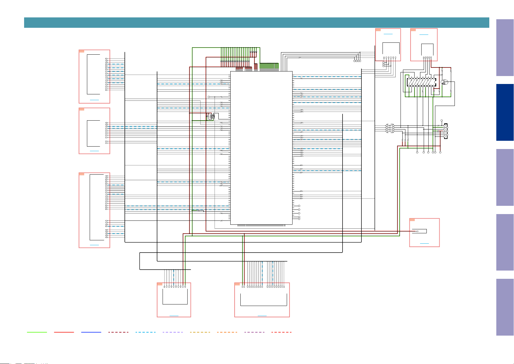
SCH08_PLD
PLD PA RT
D3
FROM LEGO P ART
TO 3D
1B
RXB CK/D SDS CK
RXM CK/D SDM CK
MN864788_H AINT
FROM H D MI_T X PA RT
TO B1
9C
TO D IR PART
TO C9
SPD IF_OU T
MCL K_I2S _0
LRCK _I2S _0
SDIN _I2S _0
SCLK _I2S _0
SDO UT_ I2S_0
LRCK _I2S _1
SDIN _I2S _1
SCLK _I2S _1
SDO UT_ I2S_1
LRCK _I2S _2
SDIN _I2S _2
SCLK _I2S _2
SDO UT_ I2S_2
PWM _3
GPIO _0
GPIO _1
GPIO _2
TXB CK
TXL RCK
TXI2 S0
RXI2 S0/D SD1
RXI2 S1/D SD2
RXI2 S2/D SD3
RXI2 S3/D SD4
RXL RCK/ DSD 5
SPD IF_OU T
HD MISPD IF
DIRM CK
DIRB CK
DIRL RCK
DIRD ATA
MPIO _B3
MPIO _B2
MPIO _B1
MPIO _B0
DIRA UXD ATA
DIRA UXL RCK
DIRA UXB CK
DIRA UXM CK
DIRX MCK
DIRS LRCK
DIRS BCK
DIRN PCM
DIRP ERR
PLD ADC BCK
PLD ADC MCK
PLD ADC LRCK
PLD ADC DAT A
Z2D ACMC K
Z2D ACBC K
Z2D ACD ATA
Z2D ACLR CK
Z2D ACMU TE
SPDIF _OUT
MCLK _I2S_ 0
LRCK _I2S_ 0
SDIN_ I2S_ 0
SCLK _I2S_ 0
SDOU T_I2 S_0
LRCK _I2S_ 1
SDIN_ I2S_ 1
SCLK _I2S_ 1
SDOU T_I2 S_1
LRCK _I2S_ 2
SDIN_ I2S_ 2
SCLK _I2S_ 2
SDOU T_I2 S_2
PWM_ 3
GPIO_ 0
GPIO_ 1
GPIO_ 2
SPDIF _OUT
HDM ISPD IF
DIRMC K
DIRB CK
DIRLR CK
DIRD ATA
MPIO_ B3
MPIO_ B2
MPIO_ B1
MPIO_ B0
DIRAU XD ATA
DIRAU XLR CK
DIRAU XBC K
DIRAU XMC K
DIRX MCK
DIRSL RCK
D
IRSBC K
DIRNP CM
DIRPE RR
PLDA DCB CK
PLDA DCM CK
PLDA DCL RCK
PLDA DCD ATA
Z2DA CMC K
Z2DA CBC K
Z2DA CDA TA
Z2DA CLRC K
Z2DA CMU TE
APLD _CS
APLD _DA TA
APLD _CLK
DIRSB CK
DIRSL RCK
GPIO_ 0
GPIO_ 1
GPIO_ 2
SDIN_ I2S_ 2
SCLK _I2S_ 2
SDOU T_I2 S_2
PWM_ 3
DIRAU XBC K
SDIN_ I2S_ 1
RXI2S 0/D SD1
RXI2S 1/D SD2
RXI2S 2/D SD3
RXI2S 3/D SD4
RXLR CK/D SD5
RXBC K/D SDSC K
RXMC K/D SDMC K
MN864788_HA INT
TXLR CK
TXB CK
TXI2 S0
DSP_ FLAG 3
DSP1 INBC K
DSP1 INSW C_C
DSP1 INF_F L
DSP1 OUT S
DSP1 OUT CSW1
DSP1 OUT BCK
DSP1 INS_S L
DSP1 INRSV _FR
DSP1 INSB _SR
DSP1 OUT F
DSP1 OUT FH
DSP1 OUT FW
RXLR CK/D SD5
RXBC K/D SDSC K
DSP1 INRSV _SW
DSP1 INMC K
DSP1 INLRC K
DSP1 OUT SB
DSP1 OUT LRCK
RXI2S 1/D SD2
RXI2S 0/D SD1
RXMC K/D SDMC K
RXI2S 3/D SD4
PLDE RR2
MN864788_HA INT
RXI2S 3/D SD4
RXI2S 2/D SD3
TXI2 S0
TXLR CK
TXB CK
Before Servicing
6C
TO C6
FROM MC U P ART
0.1uF
0.1uF
0.1uF
C7720
C7717 0. 1uF
C7719
0.1uF
0.1uFC7703
C7705 0.1uF
C7704 0.1uF
C7702
C7701 0.1uF
C7706 0.1uF
C7708 0.1uF
C7707 0.1uF
A2
IO-001
A4
IO-002
A5
IO-003
R7701 100
A6
IO-004
R7702 100
A7
IO-005
R7703 100
A8
IO-006
A9
IO-007
A10
IO-008
A11
IO-009
A12
IO-010
A13
IO-011
R7781OPE N
4
1
2 3
R7704 100
R7705 100
R7706 100
R7707 100
X7701
22.5792MHz
R7708 220
R7709 100
R7710 100
R7711 100
R7713 220
R7714 100
R7715 33
R7716 33
R7717 33
R7719 100
R7720 33
A15
IO-012
B1
IO-
013
B3
IO-014
B4
IO-015
B5
IO-016
B6
IO-017
B8
IO-018
B9
IO-019
B10
IO-020
B11
IO-021
B12
IO-022
B13
IO-023
B14
IO-024
B16
IO-025
C2
IO-026
C3
IO-027
C4
IO-028
C5
IO-029
C6
IO-030
C7
IO-031
C8
IO-032
C9
IO-033
C10
IO-034
C11
IO-035
C12
IO-036
C13
IO-037
C14
IO-038
C15
IO-039
D1
IO-040
D2
IO-041
D3
IO-042
D4
IO-043
D5
IO-044
D11
IO-045
D12
IO-046
D13
IO-047
D14
IO-048
D15
IO-049
D16
IO-050
E1
IO-051
E2
IO-052
E3
IO-053
E4
IO-054
E13
IO-055
E14
IO-056
E15
IO-057
E16
IO-058
F1
IO-059
F2
IO-060
F3
IO-061
F13
IO-062
F14
IO-063
F15
IO-064
F16
IO-065
G1
IO-066
G2
IO-067
G3
IO-068
G14
IO-069
G15
IO-070
G16
IO-071
H1
IO-072
H2
IO-073
H3
IO-074
H5
IO-075
H12
IO-076
H14
IO-077
H15
IO-078
H16
IO-079
J1
IO-080
PLD_ ERR
0.1uF
C7722
R7718
10k
C7718
C7716 0.1uF
C7715 0.1uF
C7714 0.1uF
C7713 0.1uF
C7712 0.1uF
C7711 0.1uF
C7710 0.1uF
C7709 0.1uF
J11
G10
F8
L9
L8
A14
H6
A3
C1
J6
P1
T14
C16
T3
VCCIO1-5
VCCIO1-4
VCCIO2-1
VCCIO2-3
VCCIO2-2
VCCIO1-1
VCCIO1-3
VCCIO1-7
VCCIO1-6
VCCIO1-2
VCCIO1-8
G9
G8
G7
H10
H11
J9
H8
H9
H7
A16
B2
B15
J7
P16
A1
B7
O2-6
GND-09
GND-08
GND-07
GND-06
GND-11
GND-01
GND-10
GND-02
GND-03
GND-04
GND-05
VCCIO2-7
VCCIO2-4F9VCCIO2-5
VCCINT-4
VCCINT-1
VCCINT-2
VCCI
VCCINT-3
VCCIO2-8
IC771
5M570ZF256C 5N
NC-26
NC-20
NC-19
NC-25
NC-24
NC-18
NC-35
NC-12
NC-13
NC-05
NC-11
NC-04
NC-10
NC-02D8NC-03
NC-09
NC-14
NC-01
NC-08
NC-06E6NC-07
F4
E9
E8
E7
E5
D9
D7
D6
E12
E11
E10
D10
NC-34
NC-17
NC-16
NC-23
NC-15
NC-33
NC-22
NC-30
NC-32
NC-21
NC-29
NC-28
NC-31
NC-27
J4
F7
F5
F6
K6
K5
K4
G6
G5
G4
H4
J13
F12
F11
F10
K12
K11
G13
G12
G11
H13
K10
K9
J10
K8
K7
J8
T16
R15
T1
R2
GND-17
GND-13
GND-16
GND-15
GND-12
GND-14
GND-18
GND-21
GND-19
GND-20
NC-36
NC-41
NC-40
NC-39
NC-43
NC-38
NC-45
NC-42
NC-37
NC-44
L7
L5
M7
M6
L12
L11
L10
K13
M12
M11
M10
R7748
100
L6
M5
N4
P3
TDI
TCK
TMS
TDO
J2
IO-081
J3
IO-082
R7721 0
J5
IO-083
J12
IO-084
J14
IO-085
J15
IO-086
J16
IO-087
K1
IO-088
K2
IO-089
K3
IO-090
R7722 100
K14
IO-091
R7723 100
K15
IO-092
R7724 100
K16
IO-093
L1
IO-094
L2
IO-095
L3
IO-096
L4
IO-097
L13
IO-098
L14
IO-099
R7725 0
L15
IO
-100
R7726 100
L16
IO-101
M1
IO-102
M2
IO-103
M3
IO-104
M4
IO-105
M8
IO-106
R7727 100
M9
IO-107
M13
IO-108
M14
IO-109
M15
IO-110
M16
IO-111
R7728 100
N1
IO-112
N2
IO-113
R7729 100
N3
IO-114
R7730 100
N5
IO-115
R7731 100
N12
IO-116
N13
IO-117
N14
IO-118
N15
IO-119
N16
IO-120
R7732 100
P2
IO-121
R7733 100
P4
IO-122
R7734 100
P5
IO-123
R7735 33
P6
IO-124
R7736 33
P7
IO-125
P8
IO-126
P9
IO-127
P10
IO-128
P11
IO-129
R7737 100
P12
IO-130
P13
IO-131
R7738 33
P14
IO-132
P15
IO-133
R7739 100
R1
IO-134
R3
IO-135
R4
IO-136
R5
IO-13
7
R6
IO-138
R7
IO-139
R8
IO-140
R9
IO-141
R10
IO-142
R11
IO-143
R7740 100
R12
IO-144
R13
IO-145
R7742 100
R14
IO-146
R7743 100
R16
IO-147
R7744 O PEN
T2
IO-148
T4
IO-149
T5
IO-150
T6
IO-151
T7
T7
IO-152
T8
IO-153
T9
T9
IO-154
T10
IO-155
T11
T11
IO-156
T12
IO-157
T13
T13
IO-158
T15
T15
IO-159
NC-52
NC-51
NC-46
NC-50
NC-49
NC-47N7NC-48
N9
N8
N6
N11
N10
DACP CMS B
DACP CMS
DACB CK
DACP CMF
DACL RCK
DACM CK
DACP CMC SW1
DZF1
J_TD O1
SCLK _I2S_ 1
SDOU T_I2 S_1
LRCK _I2S_ 2
SCLK _I2S_ 0
SDOU T_I2 S_0
LRCK _I2S_ 1
DIRAU XMC K
DIRAU XLR CK
DIRAU XD ATA
MCLK _I2S_ 0
LRCK _I2S_ 0
SDIN_ I2S_ 0
DIRPE RR
DIRNP CM
DIRX MCK
HDM ISPD IF
MPIO_ B0
MPIO_ B1
DIRLR CK
DIRD ATA
Z2DA CDA TA
MPIO_ B3
MPIO_ B2
DIRMC K
DIRB CK
PLDA DCM CK
PLDA DCL RCK
Z2DA CLRC K
PLDA DCB CK
PLDA DCD ATA
Z2DA CBC K
Z2DA CMU TE
Z2DA CMC K
JTAG _TMS
JTAG _TDI
JTAG _TCK
TDO 1_TDI2
J_TD I1
J_TC K1
J_TM S1
CS
APLD _
APLD _DA TA
APLD _CLK
MVOL _MUT E
VOLU ME_M UTE
PLDE RR
PLDE RR
AP_C S
AP_D A
AP_C K
VOLU ME_M UTE
MVOL _MUT E
JTAG _TCK
TDO 1_TDI2
JTAG _TDI
JTAG _TMS
POWE R_CO NTRO L
APLD _CL K
APLD _D ATA
PLD ERR
APLD _CS
RN771
100x4
1234
D6
TO 6D
This Unit
FROM LEG O PAR T
_TD O
MVO L_MU TE
VOL UME_ MUTE
10
11 12 15 16 17 18 19 201413
NET 3.3V
L_JT AG
L_JT AG_T MS
L_JT AG_T CK
L_JT AG_T DI
4k7
1k
R7776
R7777
123456789
OE1
OE2
IC772
Q7701
HVT KRC102S
SN74LV C244APW R
0
10k
OPEN
0.1uF
R7778
C7759
R7780
R7779
Electrical Mechanical Repair Information Updating
J_TC K
R7782
0
5678
R7745 1k
R7746 10k
R7747 10k
J_TD I
J_TD O
7B
PLD 1.8V
TO B7
1
1.JTA G_TC K
2
2.D GND
3
3.JTA G_TD OO
C7721
4
4.VC C
100pF
5
5.JTA G_TM S
6
6.JTA G_TD I
7
7.PL D_W RITE
CN771
CJP07GA 333ZR
MP :O PEN
DGND
J_TM S
DA3V 3
PLD_ WRIT E
FRO M
DIG ITAL SUPPL Y
PA RT
EM UL AT OR
GND LINE
POWER+ LINE
POWER- LINE
ANALOG AUDIO DIGITAL AUDIO
DZF1
DACL RCK
DACP CMF
DACP CMS
DACP CMS B
DACP CMC SW1
D4
MF
DZF 1
DAC PC
DAC PCMS
DAC PCMS B
DAC PCMC SW1
TO D A C PA RT
TO 4D
TMDS SIGNAL
DACB CK
DACM CK
DAC BCK
DAC LRCK
DGND
DA3 .3V
DAC MCK
PLD_ DAC
ANALOG VIDEO
DIGITAL VIDEO
D5
OUTF W
PLDE RR2
DSP1 OUT S
DSP1 OUT SB
DSP1 OUT FH
DSP1
DSP1 OUT CSW1
DGND
DA3 .3V
PLD ERR2
DSP 1OUT S
DSP 1OUT SB
DSP 1OUT FH
DSP 1OUT FW
TO D S P P ART
16
DSP1 OUT F
DSP1 OUT BCK
DSP1 OUT LRCK
DSP 1OUT BCK
DSP 1OUT LRC K
DSP 1OUT CSW 1
TO 5D
PLD_ DSP
DSP_ FLAG 3
DSP1 INBC K
DSP1 INMC K
DSP1 INF_F L
DSP1 INS_S L
DSP1 INLRC K
DSP1 INSB _SR
DSP1 INSW C_C
DSP1 INRSV _FR
DSP1 INRSV _SW
DSP 1OUT F
DSP 1INB CK
DSP _FLA G3
DSP 1INMC K
DSP 1INF_ FL
DSP 1INS_ SL
DSP 1INLR CK
DSP 1INSB _SR
DSP 1INSW C_C
DSP 1INRS V_FR
DSP 1INRS V_SW
STBY POWERHDMI
Page 17
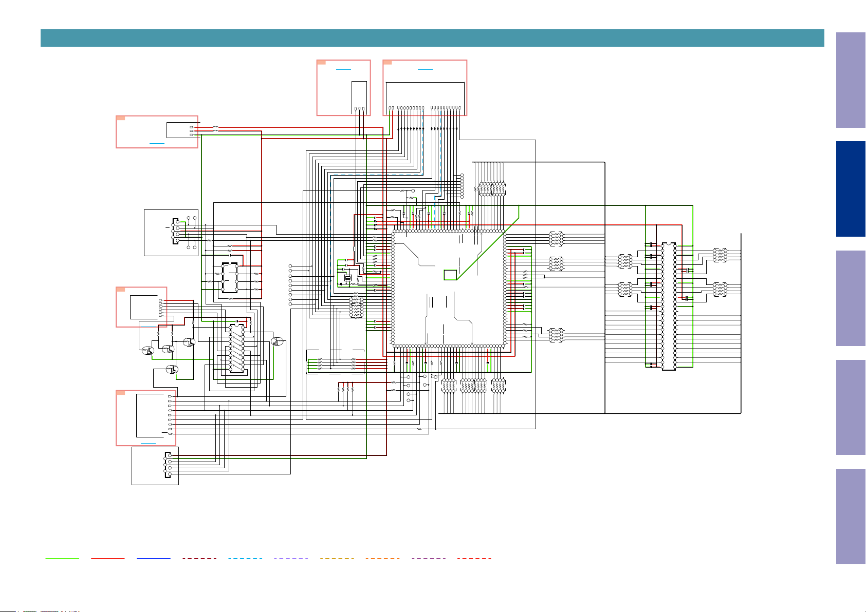
SCH09_DSP
D SP PA RT
8B
FROM
D IGIT AL SU PPLY
PA RT
TO B8
DA1 .0V
DA3 V3
DGND
L7801 CB03YT YH600
L7802 CB03YT YH600
1D
TO D1
FROM DIR PA RT
Before Servicing
5D
TO D5
FROM PLD PART
DSP 1INMC K
DSP 1OUT FH
DSP 1OUT LRC K
PLD ERR2
DSP 1OUT FW
DSP 1OUT BCK
DSP 1OUT S
DSP 1OUT F
DSP 1OUT SB
DSP 1OUT CSW 1
DGND
DA3 .3V
DA3 .3V
DGND
DSP _XT AL
DSP 1INRS V_SW
DSP 1INSB _SR
DSP 1INSW C_C
DSP 1INLR CK
DSP 1INF_ FL
DSP 1INS_ SL
DSP 1INB CK
DSP 1INRS V_FR
DSP _FLA G3
This Unit
D7
FROM LEG O
4C
NET 3.3V
DSP _CLK 2
DSP _MISO 2
DSP _MOS I2
DSP _ICS2
DSP _ROM _WR ITE2
TO 7D
Q7803
HVT KRC102S
DSP _ROM _WR ITE
DSP _FLA G3_C
FROM MC U P ART
TO C4
1.VCC( 3V3)
2.GND
3.CL K
4.MO SI
5.MIS O
6.CS 1
7.H S2
1.00mm FFC
MP : O PE N
1.00mm FFC
R7868
Q7804
HVT KRC102S
DSP _ICS
DSP _MOS I
DSP _MISO
DSP _CLK
DSP _RST
DSP _F
DSP _BSY
CN782
CJP07GA 333ZR
GND
MISO
MOS I
GND
MP : O PE N
CJP07GA 333ZR
4k7
Q7805
HVT KRC102S
LAG0
DSP _SDR AM
SD_A 0
SD_A 1
SD_A 2
SD_A 3
SD_C S
SD_A 10
SD_B A0
SD_B A1
SD_R AS
SD_C AS
DI_-/ FR
DI_-/ SW
33x4
RN782
DI_LR CK
DI_B CK
GND3
DA03_D 1, UA RTTX, G PIO3 2
BDI*, DAI1_D 0, G PIO6 4
76.SCP_ MOSI , GPIO 147
75.SCP1_C S, GP IO145
DAO3_D 2, U ARTR X, G PIO33
OPEN
T7807
C7802 0.1 uF
GND2
VDD2
BDI*, DAI1_D 1, G PIO6 5
77.VDD8
78.GND8
80.SCP1_C LK, G PIO148
79.SCP1_M ISO_ SDA, GPIO 146
DAO3_D 6, U ARTE N, GP IO35
DA03_D 5, UA RTCK , GP IO34
SD_W E, EX T_W E
R7860 33
5 6 7 8
33x4
RN784
1 2 3 4
SD_W E
SD_D QM0
DI_F/ FL
DI_C SW/C
DI_S/ SL
DI_SB /SR
R7804
EE_CS1, GPIO0
EE_CS0, GPIO 1
DAI1_D 4, GP IO68
DAI1_D 5, GP IO69
BDI* DAI1_D 3, GP IO67
BDI*, DAI1_D 2, G PIO6 6
7.SD_ BA1 , EXT _A14
8.SD_ CS,E XT_ OE
IC781
CVIC S49844A-C QZ
81.SCP1_IR Q, GP IO144_OD
82.GND9
83.VDD9
99.SD_ D1, E XT_ D9
98.SD_ D2, E XT_ D10
101.SD_ D15, EX T_D 7
100.SD_ D0, E XT_ D8
SD_D 7, E XT_D 15
SD_D 6, E XT_D 14
VDD10
GND10
SD_D QM0 , EXT _A1 5
SD_D 5, E XT_D 13
C7821 0. 1uF
5 6 7 8
1 2 3 4
RN785 33x4
SD_D 7
SD_D 6
SD_D 5
0.1uF
33
C7801
R7803 0
GND1
VDD1
4.SD_ A0, E XT_ A0
3.SD_ A1, E XT_ A1
5.SD_ A10, EX T_A 12
6.SD_ BA0 , EXT _A13
103.VDDIO4
104.GNDIO4
102.SD_ D14, EX T_D 6
SD_D 4, E XT_D 12
SD_D 3, E XT_D 11
SD_D 4
SD_D 3
SD_D 2
R7809
D_RS T
100
R7807
3k3
R7812
33
2k
C7812
10/6.3V
X7801
R7824 100
R7861 33
RN783
33x2
RN795
33x4
R7828 O PEN
R7830 O PEN
R7832 3k3R7831 O PEN
R7856 10k
R7857 10k
L7803
R7822
1
234
5 6 7 8
R7858 10k
C7846
47uF/6. 3V
C7806
100/50V
C7807 10/50V
C7808
47/10V
R7814 33
R7815 33
C7809 0.1 uF
C7810 0.1 uF
R7816 OPEN
CB03YT YH 600
7817 OPEN
R
R7819
OPEN
C7811 0.1 uF
33
R7820 OP EN
R7818
1M
24.576MHz
R7823 20k
R7821
0
C7816 0.1 uF
1 2 3 4
C7817 0.1 uF
R7862
33
C7818 0. 1uF
T7804T 7803
7
6
5
CS
4
VCC
3
2
SCK
CN781
4k7
R7869
1
2
3
4
5
6
7
1
Q7801
HVT KRC102S
R7871
0
R7842 10k
10k
R7843
T7802T 7801
4k7
R7866
R7845
OPEN
C7830
IC782
CVIEN 25QH64A 104HIP
CS
R7844
DO
HOL D
33
WP
4 3 2 1
VSS
R7846 10k
C7831 0. 1uF
SN74LV C244APW R
0.1uF
8765
VCC
CLK
DI
123456789
OE1
OE2
10
11 12 15 16 17 18 19 20141 3
IC783
DO_E XT1
DO_E XT2
R7849
10k
DI_M CK
R7848
DO_F
10k
DO_B CK
R7847
DO_L RCK
10k
DO_C
DO_S
DO_S B
4k7
R7867
Q7802
HV
TKRC 102S
C7813 0.1 uF
C7814
50V/12pF
C7815
50V/12pF
Mas ter S PI3
R7825 O PEN R7826 3k3
R7827 3k3
R7829 3k3
R7855 10k
R7806
R7813
100pF
C7805
33
R7805
2k
37
DBCK 1
38
39
40
41
VDDIO2
42
VDD4
43
GND4
44
DAI3_S CK, G PIO86
45
DAI3_D 0, GP IO84
4
6
DAI3_L CK, G PIO85
47
VDD5
48
GND5
49
XTAL _OU T
50
VDD_PL L
51
GND_PL L
52
XTI
53
XTO
54
GND6
55
VDD6
56
DAO1_M CLK , GPIO 128
57
DAO1_D 0, H S0, GPIO9 6
58
DAO1_S CK1 , GPIO 117
59
DAO1_L CK1 , GPIO 116
60
DAO1_D 1, H S1, GPIO9 7
61
DAO1_D 2, H S2, GPIO9 8
62
DAO1_D 3_XMT A,H S3,G PIO99
63
DAO1_D 4, G PIO100
64
DAO1_D 5, G PIO101
65
VDD7
66
GND7
67
VDDIO3
68
GNDIO3
69
DAO1_S CK2 , GPIO 119
70
DAO1_L CK2 , GPIO 118
71
DAO1_D 6, G PIO102
DAO1_D 7, X MTB , GPIO 103
72
73 74 75 76 77 78 79 80 8 1 82 8 3 84 85 86 87 88 89 90 91 92 93 94 95 96 97 9 8 99
4k7
R7833
R7836
3k3
R7837
3k3
C7803 0.1 uF
C7804 0.1 uF
RESET
DBCK 0
VDD3
DBD A0
DBD A1
VDDIO1
GNDIO1
DAI1_SC LK2, GPIO 73
DAI1_LR CK2, GPIO 72
BDI*, DAI1_S CLK 1, GPI O71
BDI*, DAI1_L RCK 1, GP IO70
37.SCP2_M ISO_ SDA
38.SCP2_M OSI
39.SCP2_C LK
40.GNDIO2
73.DAO 3_D7, XMTB , GPI O115
74.SCP2_C S
SCP_ BSY, GPIO 143_OD
R7859
C7820 0. 1uF
R7835 33
C7819 0.1uF
D_FL G0
D_CS
D_BS Y
D_MO SI
D_CK
D_MI SO
R7870
OPEN
R7801 33
R7802 33
1011121314151 6171819202122232 425262728293031323 3343536
TEST _EN
SD_C AS,EX T_C S2
SD_R AS,EX T_C S1
SD_A 8, EX T_A 8
SD_A 9, EX T_A 9
SD_A 11, EXT _A1 0
SD_A 12, EXT _A1 1
SD_C LKEN , EXT _A1 7
2.SD_ A2, E XT_ A2
1.SD_ A3, E XT_ A3
SD_C LKIN , EXT _A1 8
SD_C LKO UT, E XT_ A19
SD_D QM1 , EXT _A1 6
108.DAO 3_D3, XMTA , GPI O113
105.SD_ D13, EX T_D 5
106.SD_ D12, EX T_D 4
107.SD_ D11, EX T_D 3
DAO3_S CK1 ,GPIO 125
DAO3_L CK,G PIO124
DAO3_D 4,G PIO114_OD
SD_D 8, E XT_D 0
DAO3_S CK2 , GPIO 127_OD
SD_D 9, E XT_D 1
DAO3_L CK2 , GPIO 126_OD
SD_D 10, EX T_D 2
DAO3_D 0, G PIO112
100 101 102 103 104 105 106 107 108
C7822 0. 1uF
5 6 7 8
1 2 3 4
SD_D 15
SD_D 1
SD_D 0
SD_D 14
1234
5678
SD_A 4, EX T_A 4
SD_A 5, EX T_A 5
SD_A 6, EX T_A 6
SD_A 7, EX T_A 7
GND_FS
VDD_VG
DAO3_M CLK ,GPIO 130
5 6 7 8
1 2 3 4
RN786 33x4
SD_D 13
1234
33x4
RN781
5678
RN790
123456789
144
143
142
141
140
GNDIO6
C7829 0. 1uF
139
VDDIO6
C7828 0. 1uF
138
VDD14
137
GND14
136
135
134
133
R7841 33
132
R7840 33
131
R7839 33
130
129
GND13
C7827 0. 1uF
128
VDD13
R7838 33
127
126
C7826 0. 1uF
125
C7825 0. 1uF
124
VDD12
123
GND12
122
GND11
C7824 0. 1uF
121
VDD11
C7823 0. 1uF
120
VDDIO5
119
GNDIO5
118
117
116
R7865 10k
115
114
R7864 10k
113
112
R7863 10k
111
110
109
RN787 33x4
SD_D 11
SD_D 12
33x4
7 8
1 2 3 4
5 6
RN789
33x4
8
3 4
1 2
5 6 7
1 2 3 4
5 6 7 8
RN788
33x4
SD_A 11
SD_C LKEN
SD_C LKO UT
SD_D QM1
SD_D 10
SD_A 4
SD_A 5
SD_A 6
SD_A 7
SD_D 0
SD_A 8
SD_D 1
SD_A 9
SD_D 2
6 7 8
2 3 4
SD_D 3
1
5
RN791
33x4
SD_D 4
4
SD_D 5
3
SD_D 6
SD_D 7
5 6 7 8
1 2
RN792
33x4
SD_D QM0
SD_W E
SD_C AS
SD_R AS
SD_C S
SD_D 8
SD_B A0
SD_D 9
SD_B A1
SD_A 10
SD_A 0
SD_A 1
SD_A 2
SD_A 3
IC784
C7832
CVIM12L 64164A-5T G2Y
1000P
123456789
VDD
C7833
0.1uF
VSS
DQ0
DQ15
C7834
0.1uF
VDDQ
VSSQ
51 52 53 54
DQ1
DQ14
C7835
1000P
C7836
0.1uF
C7837
1000P
C7838
0.1uF
C7839
1000P
C7840
1000P
C7841
0.1uF
C7845
DQ2
DQ13
0.1uF
VSSQ
VDDQ
DQ3
DQ12
C7844
1000P
DQ4
DQ11
VDDQ
46 47 48 49 50
VSSQ
1011121 3141516171 8192021222 324252627
DQ5
DQ10
44 45
DQ6
DQ9
C7843
0.1uF
VSSQ
VDDQ
42 43
DQ7
DQ8
C7842
1000P
41
VDD
VSS
LDQM
NC
39 40
WE
UDQM
CAS
CLK
RAS
CKE
36 37 38
CS
NC
35
BA0
A11
BA1
A9
A10/AP
33 34
A8
A0
A7
A1
A6
A2
A5
A3
A4
28 29 30 31 32
VDD
VSS
DSP _SDR AM
SD_D 15
SD_D 14
SD_D 13
SD_D 12
1 2 3 4
5 6 7 8
RN794
33x4
S
D_D 11
SD_D 10
SD_D 9
SD_D 8
1 2 3 4
5 6 7 8
RN793
33x4
SD_D QM1
SD_C LKO UT
SD_C LKEN
SD_A 11
SD_A 9
SD_A 8
SD_A 7
SD_A 6
SD_A 5
SD_A 4
Electrical Mechanical Repair Information Updating
GND LINE
POWER+ LINE
POWER- LINE
ANALOG AUDIO DIGITAL AUDIO
TMDS SIGNAL
ANALOG VIDEO
DIGITAL VIDEO
STBY POWERHDMI
17
Page 18
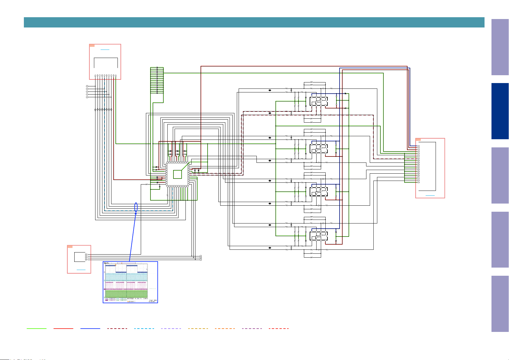
SCH10_MAIN DAC
Before Servicing
This Unit
4D
TO D4
MAIN DA C PA RT
FROM PLD PAR T
C7985
0.1uF
C7986
0.1uF
C7987
1000pF
C7988
R7902
1k
C7989
C7990
C7991
C7992
C7993
C7994
C7995
C7996
C7997
C7998
C7999
C7927
C7930 470/16V
C7929 0.1uF
C7936 100V/ 1uF
(3) DAC input
CH1:DACLRCK
(DAFS1)
CH2:DACBCK
(DA64FS1)
CH3:DACPCMF
(DADATAF1)
CH4:DACMCK
(DA256FS1)
1000pF
OPEN
OPEN
1000pF
1000pF
1000pF
0.1uF
0.1uF
0.1uF
1000pF
1000pF
1000pF
C7926
220/16V
220/16V
220/16V
C7918
C7920
C7925
C7919
C7917
0.1uF
0.1uF
0.1uF
AOUTL 3N
VREFL3
VREFH 3
AOUTL 3P
AOUTR 3N
AVSS
AOUTR 2N
VREFL2
AOUTL 2N
AVDD
AOUTR 2P
VREFH 2
2526272829303 13233343536
LRCK/ DSD L1
IC791
AK4458V N
SDTI2 /DSD L2
SDTI1 /DSD R1
SDTI3 /DSD R2/ TDM O1
24
AOUT L2P
23
AOUT R1P
22
AOUT R1N
21
VREFH 1
C7916
20
VREFL1
0.1uF
220/16V
C7915
19
AOUT L1N
18
AOUT L1P
17
I2C
16
PS
15
CAD0_I2 C
14
CL/CCLK/T DM1
13
SDA/C DTI /TDM 0
10 11 12
DSDL 4
CAD1
DSDR 4
DSDR 3
DZF/S MUTE
SDTI4 /DSD L3/ TDM O2
DA_D A1
DA_C K1
DA_M S1
37
AOUT R3P
C7928
220/16V
38
AOUT L4P
39
AOUT L4N
40
VREFH 4
0.1uF
41
VREFL4
42
AOUT R4N
43
AOUT R4P
44
LDOE
45
TVDD
46
DVSS
47
VDD18
48
PDN
1 2 3 4 5 6 7 8 9
C7935
0.1uF
MCLK
BICK/ DCLK
33
R7901
3k9/ F-T
3k9/ F-T
3k9/ F-T
3k9/ F-T
3k9/ F-T
3k9/ F-T
3k9/ F-T
3k9/ F-T
3k9/ F-
3k9/ F-T
3k9/ F-T
3k9/ F-T
3k9/ F-T
3k9/ F-T
3k9/ F-T
3k9/ F-T
R7911
R7912
R7921
R7922
R7931
R7932
R7941
R7942
R7951
R7952
R7961
R7962
R7971
R7972
R7981
R7982
R7916 33k
R7917 4k 7/F-T
C7913
V-
A-INPUT
A+INPUT
+
B
-
B+INPUT
B-INPUT
5 6 7 8
C7923
680pF
(GRM21)
V-
A-INPUT
A+INPUT
+
B
-
B+INPUT
B-INPUT
5 6 7 8
C7933
680pF
(GRM21)
T
V-
A-INPUT
A+INPUT
+
B
-
B+INPUT
B-INPUT
5 6 7 8
C7963
680pF
(GRM21)
V-
A-INPUT
A+INPUT
+
B
-
B+INPUT
B-INPUT
5 6 7 8
C7983
680pF
(GRM21)
R7919
680pF
100
(GRM21)
1234
-
A
A OUTPUT
+
IC792
V+
B OUTPUT
NJM8080G
R7929
100
C7943
R7939
100
470pF
(GRM21)
1234
C7934
-
A
A OUTPUT
+
IC793
V+
B OUTPUT
NJM8080G
C7944
R7949
100
C7953
R7959
680pF
100
(GRM21)
1234
C7954
-
A
A OUTPUT
+
IC794
V+
B OUTPUT
NJM8080G
C7964
R7969
100
C7973
R7979
100
680pF
(GRM21)
1234
C7974
-
A
A OUTPUT
+
IC795
V+
B OUTPUT
NJM8080G
C7984
R7989
100
R7918 180
C7911
(GRM21)
R7915
3900pF
180
33k
R7914
C7912
R7913
680pF
4k7/ F-T
33k
(GRM21) (GRM21)
R7923
R7924
C7922
680pF
4k7/ F-T
R7925
C7921
180
3900pF
R7928 180
(GRM21)
R7927
4k7/ F-T
R7926 33k
R7946 47k
R7947 10k/F-T
R7948 150
C7931
(GRM21)
R7945
3900pF
150
47k
(GRM21)
470pF
R7943
R7944
C7942
10k/F-T
33k
R7934
R7933
C7932
680pF
(GRM21)
4k7/ F-T
R7935
C7941
180
R7938 180
3900pF
(GRM21)
R7937
4k7/ F-
R7936 33k
R7956 33k
R7957 4k 7/F-T
R7958 180
C7951
(GRM21)
T
R7955
3900pF
180
33k
680pF
R7954
R7953
C7952
4k7/ F-T
33k
(GRM21) (GRM21)
680pF
R7964
C7962
R7963
4k7/ F-T
R7965
C7961
180
R7968 180
3900pF
(GRM21)
R7967
4k7/ F-T
R7966 33k
R7976 33k
R7977 4k 7/F-T
R7978 180
C7971
(GRM21)
R7975
3900pF
180
33k
680pF
R7974
C7972
R7973
4k7/ F-T
33k
(GRM21) (GRM21)
680pF
R7984
C7982
R7983
4k7/ F-T
R7985
C7981
180
R7988 180
3900pF
(GRM21)
R7987
4k7/ F-T
R7986 33k
FR
C7901
220/25V
OPEN
C7914
OPEN
C7924
C7902
220/25V
FL
Electrical Mechanical Repair Information Updating
SW
OPEN
OPEN
C
SR
OPEN
OPEN
D8
-12V
+12V
DA+ 5V
AGND
AGND
DAC FR
AGND
DAC FL
AGND
DAC SW
AGND
DAC C
AGND
DAC SR
AGND
DAC SL
AGND
DAC SBR
AGND
DAC
AGND
FROM AU DIO PART
SBL
TO 8D
SL
SB R
OPEN
OPEN
SB L
DGND
DAC MCK
DAC PCMS B
DAC PCMS
DA3 .3V
DAC PCMC SW1
DAC PCMF
DAC BCK
DAC LRCK
DZF 1
DA_Z _MU TE1
DAD ATAF 1
DAFS 1
DA64FS 1
DA256FS 1
5C
DAC _RST
DAC _DA TA
DAC _CLK
DAC _MS
TO C5
FROM MC U P ART
GND LINE
POWER+ LINE
POWER- LINE
ANALOG AUDIO DIGITAL AUDIO
TMDS SIGNAL
ANALOG VIDEO
DIGITAL VIDEO
STBY POWERHDMI
18
Page 19
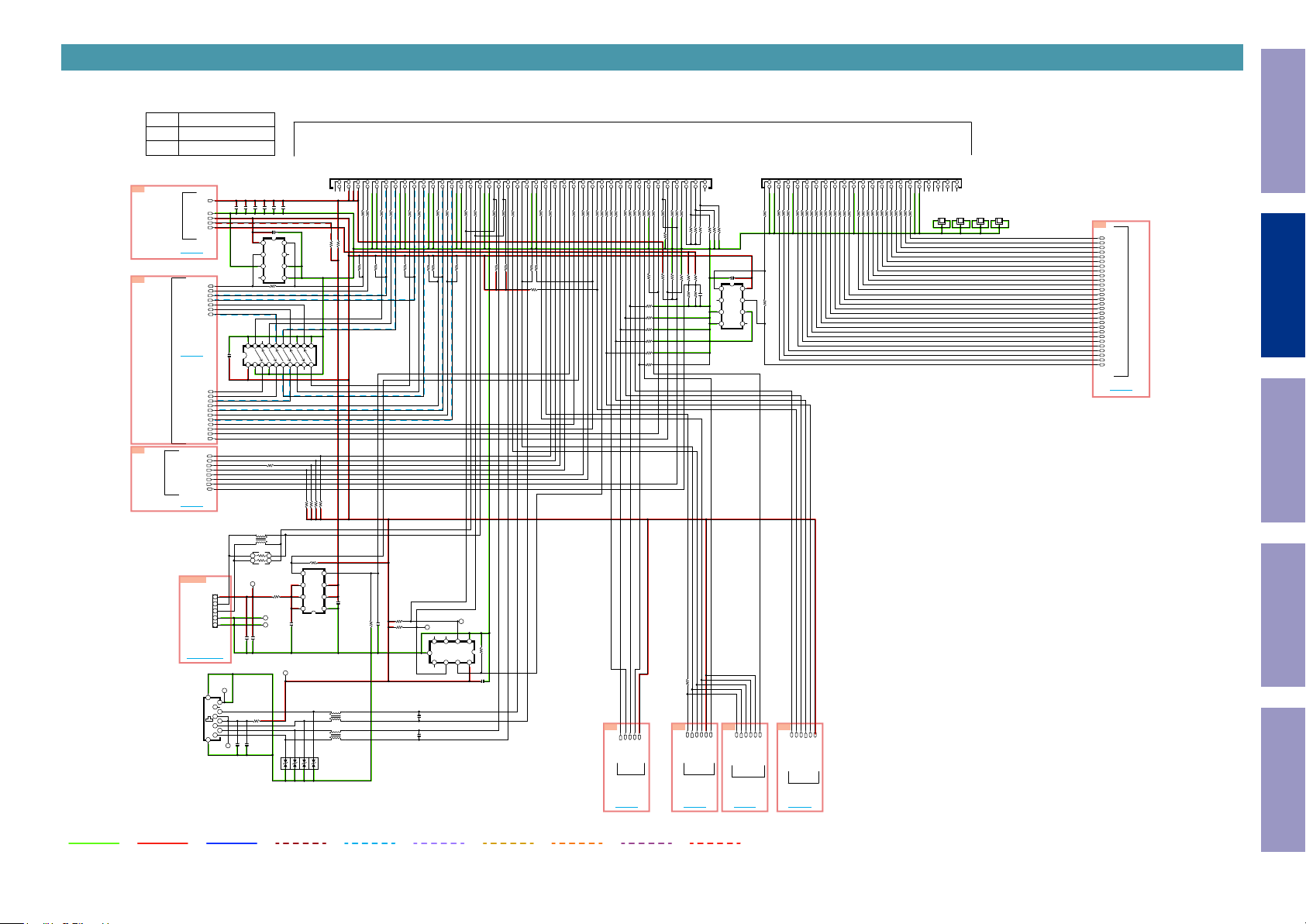
SCH11_NETWORK
Before Servicing
This Unit
LE GO OU TP UT
I2S _0
I2S _1
D SD OU TP UT (T BD )
I2S _2
LE GO INP UT (Z one 2)
6B
3D
FRO M PO WER SUPPLY
LEGO 5V
NET 3.3V
SWM 3.3V
TO B6
MCLK _I2S_ 0
SPDIF _OUT
SDIN_ I2S_ 0
SDIN_ I2S_ 1
LRCK _I2S_ 1
SCLK _I2S_ 1
SDOU T_I2 S_1
DGND
D5V
TO D3
TO P LD P ART
LRCK _I2S_ 0
SCLK _I2S_ 0
SDOU T_I2 S_0
LRCK _I2S_ 2
SDIN_ I2S_ 2
SCLK _I2S_ 2
SDOU T_I2 S_2
PWM_ 3
GPIO_ 0
GPIO_ 1
AIOS4_S TBY _STA TUS
FROM MCU
GPIO_ 2
E_RX D_M IEO
E_CT S_MIE O
E_TX D_M OEI
E_RT S_MO EI
AIOS4_W AKE UP
NET_ FACT _RST
TEMP _SEN SOR
TO C3
CN813
TO BN104
JK811
CJJ9L029Z
KRJ-015XXN L
FROM US B P CB
CN813
CJP05GI 288ZY
SMAW200-05P
VBUS
USBD +
USBD -
DGND
DGND
9
10
3C
4.7/6 .3V
4.7/6 .3V
4.7/6 .3V
C8103
C8102
C8101
IC811
OPEN
OE1
IC812
OE2
C8108 0.1uF
SN74LV C244APW R
R8168 0
L8102
34
RN811
0x2
T224
T222
T223
5 4 3 2 1
OPEN
0.1uF
C8110
C8111
T225
8
7
6
5
R8181
4
OPEN
3
2
1
C8118
OPEN
OPEN
C8117
T20
80 Pin CO NNECTO R
C8104
C8107
8765
R8101 0
OPEN
CJP80GA 370ZU
0.1uF
0.1uF
0.1uF
C8106
C8105
OPEN
1A
VCC
1Y
3Y
3A
2A
4 3 2 1
GND
2Y
10
987654321
131420 19 18 17 16 15 12 11
R8170 O PEN
R8169 O PEN
12
R8173 10k
/OC
OUT
R8182
OUT
0
8 7 6 5
OUT
IC814
BD82065FV J-E2
1uF
C8112
T326
OPEN
OPEN
OPEN
OPEN
D8101
D8102
D8103
D8104
CN811
R8171 O PEN
GND
R8172 O PEN
EN
IN
IN
R8174 O PEN
4321
L8103
EXC34C E900U
L8104
EXC34C E900U
1. NC
2. NC
3. NC
3 567891011
214
NC
NC
NC
R8175 0
1uF
C8113
6. 5V 0
5. 5V 0
4. 5V 0
8. AI OS4_SP DIF_ OUT
13. AIO S4_SCL K_I2 S_0
17. AIO S4_LRC K_I2 S_1
20. AIO S4_I2S_1_O UT
7. AI OS4_MC LK_I 2S_0
9. GND
11. AIO S4_LRC K_I2 S_0
12. AIO S4_I2S_0_I N
14. AIO S4_I2S_0_O UT
10. GND
15. GND
16. GND
13 15
12 14
16 26
0
R8104 33
R8105 33
R8106
R8103 33
R8102 33
R8001 10k
R8002 10k
R8003 10k
R8178
2k2
OPEN
R8179
2k2
C8115
R8177 10k
18. AIO S4_I2S_1_I N
17
0
R8107
IC815
MFI337S3959
C8119
C8120
19. AIO S4_SCL K_I2 S_1
21. GND
R8004 OPEN
T90
9
OPEN
OPEN
23. AIO S4_LRC K_I2 S_2
24. AIO S4_I2S_2_I N
25. AIO S4_SCL K_I2 S_2
26. AIO S4_I2S_2_O UT
22. GND
2523
242221201918
0
0
R8109
R8108
R8005 10k
R8006 OPEN
4 3 2 1
NC
NC
SCL
NC
27. GND
29. AIO S4_I2C_0_S DA
28. GND
282730
R8110 33
T91
SDA
RST
39. AIO S4_SPI_ SS
30. AIO S4_USB _DM
31. AIO S4_I2C_0_S CL
32. AIO S4_USB _DP
33. GND
35. AIO S4_I2C_1_S DA
36. AIO S4_TP0_N
37. AIO S4_I2C_1_S CL
38. AIO S4_TP0_P
40. AIO S4_RXI_ N
42. AIO S4_RXI_ P
43. GND
45. AIO S4_SPI_ CLK
41. AIO S4_SPI_ MISO
34. GND
29 596057
32 626164
R8111 33
GND
4k7
R8180
VCC
8765
C8116
0.1uF
44. GND
35333431
OPEN
R8112
R8007 10k
4543
4442414039383736
R8113 OPEN
R8114 33
R8115 33
R8008 10k
R8009 10k
R8010 OPEN
R8011
10k
FROM LEGO MODULE
48. AIO S4_UAR T_RT S
51. AIO S4_USB _VB US_E N
53. AIO S4_USB _FAU LTN
47. AIO S4_UAR T_T X
46. AIO S4_SPI_ MOSI
4748495051
R8116 33
58. AIO S4_CP_ RESE T
49. AIO S4_UAR T_RX
50. AIO S_UA RT_C TS
52. AIO S4_PW M3
54. AIO S4_WA KE_U P
56. AIO S4_GPIO _0
59. AIO S4_GPIO _SPI _CLK
61. AIO S4_GPIO _SPI _MISO
63. AIO S4_GPIO _SPI _MOS I
55. AIO S4_STB Y_S TAT US
57. AIO S4_GPIO _SPI _SS_0
60. AIO S4_GPIO _JTA G_T DI
62. AIO S4_GPIO _JTA G_T DO
53 55
52 54
R8118 0
R8117 OPEN
63 65
58
5646
R8123 33
R8124 0
R8121 33
R8122 33
R8120 33
R8119 33
R8125 33
R8126 33
6D
L_JT AG_T DI
L_JT AG_T DO
TO P LD
TO D6
65. AIO S4_GPIO _SPI _EN_ 0
64. AIO S4_GPIO _JTA G_T CK
66. AIO S4_GPIO _JTA G_T MS
70. AIO S4_GPIO _1
67. AIO S4_GPIO _SPI _EN_ 1
68. AIO S4_GPIO _SPI _EN_ 2
69. AIO S4_GPIO _SPI _EN_ 3
68677069727174737675787780
66
R8019 10k
R8127 0
R8128 33
R8018 33
R8020 33
R8021 O PEN
R8016
10k
R8015
10k
R8014
10k
R8013
10k
R8012
10k
R8017
10k
NET 3.3V
L_JT AG_T CK
L_JT AG_T MS
(B7 )
15. AIO S4_VOU T_D 07(R7)
72. AIO S4_GPIO _2
74. AIO S4_RES ET_IN
79. AIO S4_MB_ TYP E_2
71. NC
73. NC
75. NC
76. AIO S4_MOD ULE _IS_A WAK E
77. AIO S4_MB_ TYP E
78. AIO S4_MB_ REVI SION
80. NC
79
NC
R8129 OPEN
R8024 10k
10k
R8022
R8132 56k
R8131 33k
2k7/ D
R8130 33
R8025 10k
R8133 10K/D
R8134 10K/D
R8135 10K/D
R8136 1k/D
R8138
R8137 300/D
C8109
OPEN
OPEN
R8185
TH801
THE RMIST OR 10K
1A
R8023 O PEN
NTC
OPEN
3Y
R8184
OPEN
R8183 10k
C8121
2A
4 3 2 1
GND
IC813
OPEN
3. GND
1. AI OS4_VO UT_ PCLK
8. AI OS4_VO UT_ D00(R0 )
9. AI OS4_VO UT_ D01(R1 )
10. AIO S4_VOU T_D 02(R2)
2. GND
4. AI OS4_VO UT_ VS
5. AI OS4_VO UT_ HS
6. AI OS4_VO UT_ PE
7. GND
16. AIO S4_VOU T_D 08(G0)
20. GND
1
3 56789
2 4
1011121314
R8145 33
R8146 33
R8147 33
R8144 33
R8141 33
R8142 33
R8143 33
R8139 33
8765
VCC
1Y
0
R8140
3A
2Y
21. AIO S4_VOU T_D 13(G5)
17181920212223242526272829303132333435363738394041
15
16
R8155 33
R8156 33
R8157 33
R8152 33
R8153 33
R8154 33
R8151 33
R8149 33
R8148 33
R8150 33
14. AIO S4_VOU T_D 06(R6)
13. AIO S4_VOU T_D 05(R5)
19. AIO S4_VOU T_D 11(G3)
12. AIO S4_VOU T_D 04(R4)
18. AIO S4_VOU T_D 10(G2)
17. AIO S4_VOU T_D 09(G1)
11. AIO S4_VOU T_D 03(R3)
31. AIO S4_VOU T_D 23
24. AIO S4_VOU T_D 14(G6)
30. AIO S4_VOU T_D 20(B4 )
29. AIO S4_VOU T_D 21(B5 )
23. AIO S4_VOU T_D 15(G7)
28. AIO S4_VOU T_D 18(B2 )
22. AIO S4_VOU T_D 12(G4)
27. AIO S4_VOU T_D 19(B3 )
26. AIO S4_VOU T_D 16(B0 )
32. AIO S4_VOU T_D 22(B6 )
25. AIO S4_VOU T_D 17(B1 )
33. GND
R8167 33
R8164 33
R8165 33
R8166 33
R8163 33
R8162 33
R8161 33
R8158 33
R8159 33
R8160 33
42 Pin CO NNECTO R
35. NC
36. NC
34. GND
37. NC
38. NC
39. NC
40. NC
41. NC
42. NC
CN812
42
CJP42GA 370ZU
NCNCNC
NC
NC
NCNCNC
1
BK812
BK813
BK81
VMD1 A960
VMD1 A960
VMD1 A960
BK814
VMD1 A960
4A
VOU T_D 22
VOU T_D 23
VOU T_D 20
VOU T_D 21
VOU T_D 18
VOU T_D 19
VOU T_D 16
VOU T_D 17
VOU T_D 14
VOU T_D 15
VOU T_D 12
VOU T_D 13
VOU T_D 11
VOU T_D 10
VOU T_D 09
VOU T_D 08
VOU T_D 07
VOU T_D 06
VOU T_D 05
VOU T_D 04
VOU T_D
VOU T_D 02
VOU T_D 01
VOU T_D 00
VOU T_PE
VOU T_H S
VOU T_VS
VOU T_PC LK
Electrical Mechanical Repair Information Updating
03
TO H D MI R X P AR T
TO A4
56
R8186
OSD _SPI_ MO
TO O SD
TO B2
9A
NET 3.3V
GUI_ WRIT E
OSD _SPI_ MI
OSD _SPI_ CS
OSD _SPI_ CLK
OSD _SPI_ MI
OSD _SPI_ CS
OSD _SPI_ MO
OSD _SPI_ CLK
TO
H DM I_T X
TO A9
7D
NET 3.3V
788_GUI_ WRIT E
NET 3.3V
DSP _ICS2
DSP _CLK 2
DSP _MOS I2
DSP _MISO 2
DSP _ROM _WR ITE2
TO D SP
TO D7
2B
GND LINE
POWER+ LINE
POWER- LINE
ANALOG AUDIO DIGITAL AUDIO
TMDS SIGNAL
ANALOG VIDEO
DIGITAL VIDEO
STBY POWERHDMI
19
Page 20
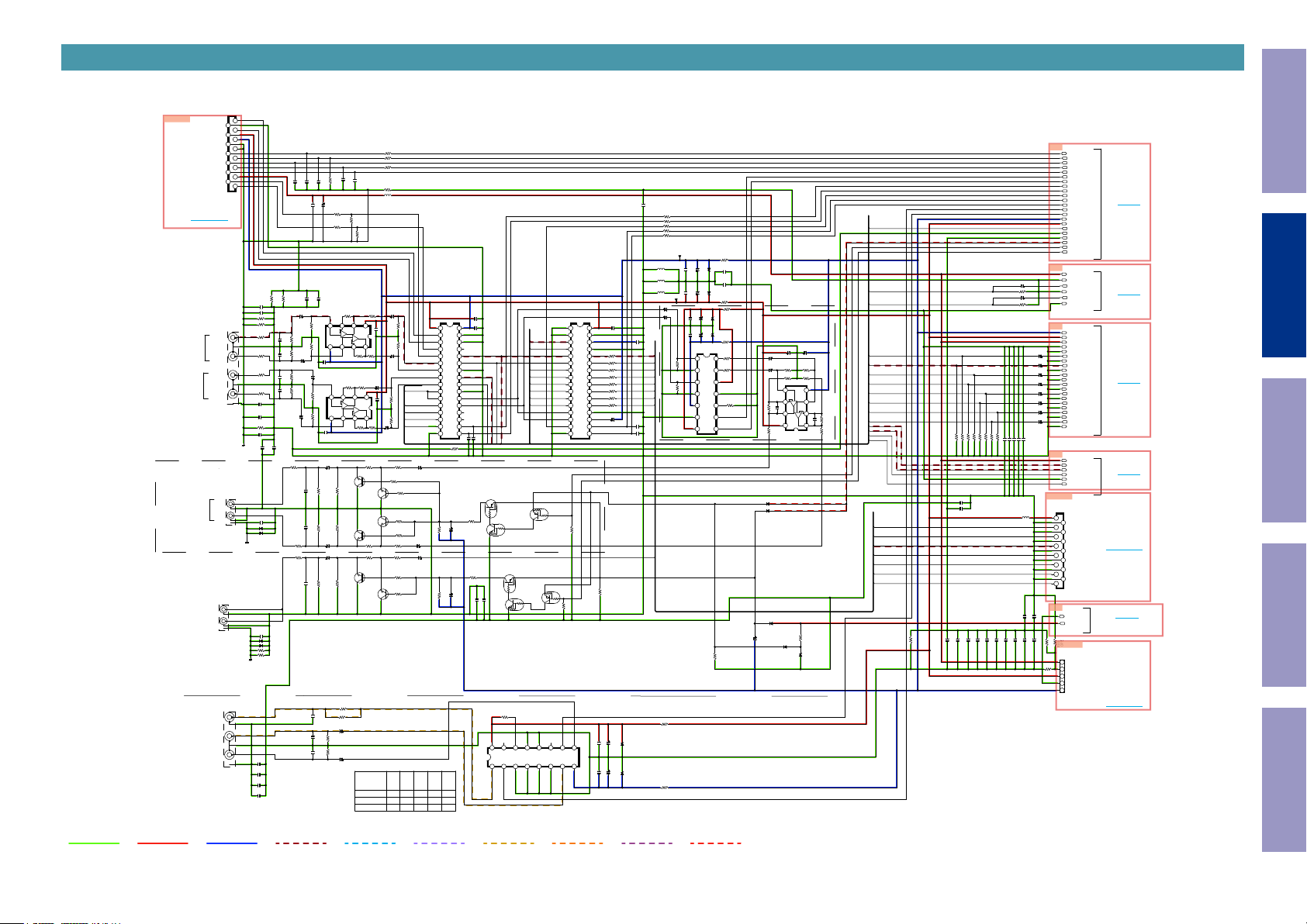
SCH12_ANALOG
ANALO G PA RT
CN821
& P H ONO
TO TUN ER MO DU LE
TO CN825
CB L/SAT
INP UT
Me dia P laye r
INP UT
AV RX 1500H E3 ON LY
ZO NE2 O UT
PRE OUT
MO NITO R
VIDE O IN
Me dia P laye r
CO MPO SIT E
VID EO PAR T
W AFE R 1 .25m m
SW 2
SW 1
CB L/SAT
PHO NO-L
AGND
PHO NO-R
+7. 5V
CH_ GND
CH_ GND
/RST
SDIO
SCLK
TUN ER-R
TUN ER-L
C125Z2-1560
CJP15H J282X
L CH
R CH
L CH
R CH
CJJ4N121Z D
CJJ4P097Z D
-7.5 V
INT
/CE
VCC
CJJ4P096Z D
CJJ
R CH
L CH
JK822
4N120ZD
1412
10
8
64
2
CN821
JK821
JK911
C8266 0.1uF
D8207 OPE N
D8208OP EN
R8268
JK881
1513
11
9
75
31
CHGND
CHGND
OPENR8269
OPEN
CHGND
C8210
0.1uF
C8211 OPEN
R8270 OPEN
R8271 0
R8213
100
R8214
100
R8217
100
R8218
100
C8212 0.1uF
C8213 0.1uF
R8221 0
C8214 OPEN
C9120
D8503 OPEN
D8504 OPEN
C8801
OPEN
C8802
OPEN
C8803
OPEN
C8804
OPEN
Before Servicing
This Unit
C8239
R8245 100
C8240
R8246 100k
C8256 0 .1uF
C8253 0 .1uF
C8255 0 .1uF
C8254 0 .1uF
L8202
CB03YT YH 600
C8830
0.1uF
0.1uF
0.1uF
C8827
C8828
2C
TU_ INT
TU_ RST
TU_ SEN
TU_ SDIO
TU_ SCLK
ZVO L_DA TA
ZVO L_CL K
SEL_ CLK
SEL_ DAT A
MVO L_MU TE
MVO L_CL K
MVO L_DA TA
VINA
VI
-12V
+12V
MIC_ SIGNAL
MIC_ GND
DGND
MUT E_3V3
ZONE 2_MUT E
PRE_ MUT E
2D
DA+ 5V
DAGND
10/50V
NET _L
k
DAGND
10/50V
NET _R
AGND
8D
-12V
+12V
DA+ 5V
AGND
AGND
DAC FR
C8245
AGND
47/50V
DAC FL
C8244
AGND
47/50V
DAC SW
C8247
AGND
47/50V
DAC C
C8246
AGND
47/50V
DAC SR
C8249
AGND
47/50V
DAC SL
C8248
AGND
47/50V
DAC SBR
C8251
AGND
47/50V
DAC SBL
C8250
AGND
47/50V
0D
DA+ 5V
Z2_AD C_L
Z2_AD C_R
ADIN L
AGND
ADIN R
CN822
CN822
CJP15H J282X
C125Z2-1560
+12V
15
1412
AGND
13
SBL
AGND
11
SBR
10
AGND
9
FL
8
AGND
75
SL
64
AGND
CEN
AGND
31
SR
2
AGND
FR
8C
RLY _GND
0.1uF
C8831
MUT E_+ B
0.1uF
0.1uF
C8829
CN823
OPEN
OPEN
R8810
R8811
CN823
CJP05GI 288ZY
SMAW200-05P
54321
5.D A+5V
R8809
4.VGND (RET _GND)
0
3.+ 12V
2.RL Y_GND
1.-12V
NB
TO CN201
TO SUB -AMP B'D
B T O B WAFE R/15P/ 1.25mm
FRO M
MC U_LE VEL_ CHG PAR T
TO BN301
FRO M MC U PA RT
FRO M DI R PAR T
DA C PA RT
DIR PAR T
TO C8
FRO M REG ULAT OR B 'D
TO C2
Electrical Mechanical Repair Information Updating
TO D2
TO D8
TO D0
WA FER/09P /2.0 mm
R8207 100
R8208 33
R8209 100
100P
10k
100P
C8204
100P
100P
0.1uF
C8205
R8222
C8203
C8201
C8202
0.1uF
C8207
C8206
0.1uF
OPEN
R8211
C8217
C8218
C8219
C8220
0.1uF
C8215
C8216
0.1uF
0.1uF
OPEN
C8208
R8212
C8209
C8267
10/50V
91k
R8272
IC823
NJM8080G
220P
100k
R8215
91k
R8273
100k
C8268
R8216
C8269
220P
10/50V
OPEN
220P
100k
R8219
C8273
10/50V
100k
220P
R8220
91k
R8280
NJM8080G
IC824
91k
R8281
C8274
10/50V
C8275
OPEN
0.1uF
C9116
R9131
220
22/50V
330P
100k
R9129
C9118
330P
100k
C9119
R9130
C9117
R9132
220
22/50V
C8264
R8267
220
22/50V
330P
100k
R8266
C8265
22P
C8807
OPEN
C8805
C8806
OPEN
470/10V
R8201
270
R8202
270
R8276
0
-
B-INPUT
B
B+INPUT
+
V-
A+INPUT
4 3 2 1
R8284
0
-
B-INPUT
B
B+INPUT
+
V-
A+INPUT
4 3 2 1
100k
R9127
100k
R9128
100k
R8265
R8803 1k8
R8804 82/F
C8808
10/50V
75/F
R8801
75/F
R8802
C8809
10/50V
R8210 O PEN
L8201
CB03YT YH 600
100k
R8203
100k
R8205
C8277
R8278
47uF/25V
100
8765
V+
OPEN
C8270
B OUTPUT
+
A
-
A OUTPUT
A-INPUT
R8277
R8279
100
0
C8279
47uF/25V
R8286
100
8765
V+
OPEN
C8276
R8290
B OUTPUT
+
A
-
A OUTPUT
A-INPUT
R8285
R8291
R8287
100
0
C8280
47uF/25V
R9125
470
R9121
10k
Q9106
HVT KTC2875B
Q9104
HVT KTC2875B
Q9105
HVT KTC2875B
Q9107
R9126
HVT KTC2875B
470
R8264
R8263
470
Q8205
HVT KTC2875B
Q8204
HVT KTC2875B
NLM2595 S/W TABL E(SW 2,5 CONT ROL)
SW1
(14)
FUNC .IN
FIX FIX FIX
H
MUT E
H
Med ia Pl aye r
H H
SAT /CBL
0.1uF
C8243
R8233 0
R8234 0
R8235 0
R8244 0
R8243 0
-7.5V
L8203
CB03YT YH 600
L8204
CB03YT YH 600
L8205
CB03YT YH 600
C9101
C8221
OPEN
C8222
V+
R8288
PHON O_L
PHON O_R
TUNER _L
470k
R8289
TUNER _R
CBL/SA T_L
C8278
CBL/SA T_R
47uF/25V
Media Pla yer_ L
Media Pla yer_ R
MIC_S IGNAL
470k
DAC_ FL
ALL_Z_ L
DAC_ FR
ALL_Z_ R
NETL
470k
NETR
C9114
R9119
470
22/50V
R9123
10k
R9124
10k
R9122
10k
C9115
R9120
470
22/50V
C8263
470
22/50V
R8261
10k
R8262
10k
SW3
SW2
(4)
(10)
L
X
(L)
X
L
X
(L)
OPEN
ADR1
ADR0
NC
MAIN_L
MAIN_R
REF_A
Z2_ADC _L
Z2_ADC _R
IC821
REF
MIC
_B
101112131 41516
CVIN JU72750AV
ZONE2_L
MIC
ZONE2_R
NC
NC
NET_L
CLOC K
NET_R
DATA
REF
17 18 19 20 21 22 23 24 25 26 27 28 29 30 31 32
OPEN
ADIN R
Z2_ADC_ R
Z2_ADC_ L
OPEN
ADIN L
C8223
C8224
R8236 0
ZONE 2_MUT E
Q9103
HVT KRA104S
R9117
1k
470k
C9113
R9118
0.1/50V
Q9102
HVT KRC104S
SW_ MUT E
R8259
1k
Q8203
HVT KRA104S
Q8202
470k
C8262
R8260
0.1/50V
SW4
SW5
(6)
(2)
L
L
L
HH(L)
L
HVT K
C8260 0.1uF
C8261 0.1uF
R8805
10k
VCC
VO2
SW1
16 15 14 13 1 2 11 10
IC881
NJM2595MT E1
VIN5
V01
SW5
V-
123456789
470k
RC104S
VIN1
SW3
DAC_ FL
DAC_ FR
DAC_ C
DAC_ SW
DAC_ SL
DAC_ SR
DAC_ SBL
DAC_ SBR
Q9101
HVT KRA104S
ZONE 2_R
ZONE 2_L
GND
VIN4
Q8201
HVT KRA104S
VO3
SW4
AREF
V+
3231302 92827262 52423222 12019181 7
ADR
AREF
DAC_ FL
V-
DAC_ FR
AREF
MAIN_L
FL
MAIN_R
FR
DAC_ C
CEN
DAC_ SW
SW
IC822
DAC_ SL
SL
9 8 7 6 5 4 3 2 1
NJU72343V
DAC_ SR
SR
DAC_ SBL
SBL
DAC_ SBR
SBR
ZONE2_L
AREF
ZONE2_R
VDDOUT
MUTE
CLOC K
REF
DAT A
16 15 14 13 12 11 10
10k
R9116
R8257
10k
R8258
SW2
VIN2
C8810
9
87654321
C8811
VIN3
VSS
C8225
R8232 47
R8231 47
R8230 47
R8229 47
R8228 47
R8227 47
R8226 47
R8225 47
C8229
47k
0.1uF
C8812
0.1uF
C8813
10/50V
C9102
10/50V
OPEN
C8226
OPEN
FL
FR
CEN
SW
SL
SR
SBL
SBR
C8227
OPEN
1/50V
C8228
OPEN
SW
R8806
270(1W)
5.1V
Z
D8801
100/50V
Z5.1V
D8802
100/50V
R8807
270(1W)
R8240
82(1W)
C8237
C8233
C8235
OPEN
D8201
Z7.5V
0.1uF
220/25V
C8238
0.1uF
R8241
+7.5V
C8234
C8236
OPEN
D8202
Z7.5V
220/25V
82(1W)
R9101
470(1W)
Z6.8V
D9101
C9105
C9103
0.1uF
100/50V
Z6.8V
D9102
R9102
C9106
C9104
0.1uF
100/50V
470(1W)
IC911
CVIBD 3812F
R9107
1234567
IN1
OUT1
100
100k
R9106
AGND
R9103
OUT2
100
IN2
SEL
100k
AGND
R9104
DGND
R9105
VEE
10 1 1 12 13 14
MUTE
AGND
DA
8 9
VCC
CL
47k
R8256
AV RX1500W E3
ON LY
C9109
C9110
C9107
10/50V
10/50V
10/50V
R9109
R9108
C9108
47k
47k
10/50V
R9111
R9110
2k2
2k2
B+INPUT
4321
V-
B-INPUT
A+INPUT
-
+
D8203 K DS160
D8204 K DS160
C8259
10/50V
KDS160
B
A-INPUT
39P
C9111
-
+
NJM8080G
A
B OUTPUT
R9112 11k
R9113
D8206
100
CVINJ M8080G
D8209
KDS160
39P
C9112
8 7 6 5
V+
A OUTPUT
IC912
R9115
820
R8255
Z3.9V
D8205
10k
MIC_ SIGNAL
NET L
NET R
DAC _FR
DAC _FL
DAC _SW
DAC _C
DAC _SR
DAC _SL
DAC _SBR
DAC _SBL
11k
R9114
Z2_AD C_L
Z2_AD C_R
100
ADIN L
ADIN R
SBL
SBR
FL
SL
CEN
SR
FR
0
R8808
C8257 0.1 uF
C8258 0. 1uF
0.1uF
C8820
R8252 100k
R8250 100k
R8251 100k
R8248 100k
R8249 100k
R8254 100k
R8247 100k
C8821
C8252 0 .1uF
R8253 100k
0.1uF
0.1uF
0.1uF
0.1uF
0.1uF
C8826
C8825
C8822
C8824
C8823
GND LINE
POWER+ LINE
POWER- LINE
ANALOG AUDIO DIGITAL AUDIO
TMDS SIGNAL
ANALOG VIDEO
DIGITAL VIDEO
STBY POWERHDMI
20
Page 21
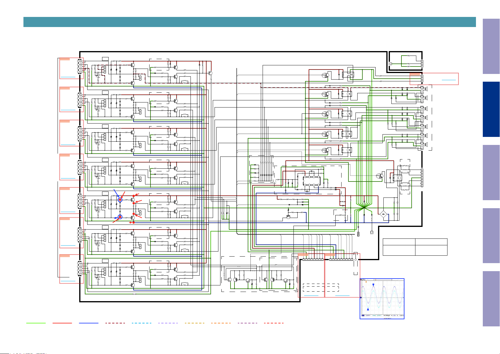
SCH13_MAIN
CN51B
TO CN51A
CN52B
TO CN52A
CN53B
TO CN53A
CN54B
TO CN54A
FRO M DI FF-AMP B'D
CN55B
TO CN55A
CN56B
TO CN56A
CN57B
TO CN57A
GND LINE
POWER+ LINE
FL I N
SL IN
CEN IN
SR IN
FR I N
SB L IN
SB R IN
M AIN PART
1
1.FB_ FL
2
2.FB_ FL
3
3.PRE _-B
4
4.PRE _-B
5
5.FL
6
6.FL
7
7.AGND
CN51B
CJP07GI281Z
CN52B
CJP07GI281Z
1
1.FB_ SL
2
2.FB_ SL
3
3.PRE _-B
4
4.PRE _-B
5
5.SL
6
6.SL
7
7.AGND
CJP07GI281Z
CN53B
1
1.FB_ CEN
2
2.FB_ CEN
3
3.PRE _-B
4
4.PRE _-B
5
5.CEN
6
6.CEN
7
7.AGND
CN54B
CJP07GI281Z
1
1.FB_ SR
2
2.FB_ SR
3
3.PRE _-B
4
4.PRE _-B
5
5.SR
6
6.SR
7
7.AGND
CN55B
CJP07GI281Z
1
1.FB_ FR
2
2.FB_ FR
3
3.PRE _-B
4
4.PRE _-B
5
5.FR
6
6.FR
7
7.AGND
CN56B
CJP07GI281Z
1
1.FB_ SBL
2
2.FB_ SBL
3
3.PRE _AGND
4
4.PRE _AGND
5
5.SBL
6
6.SBL
7
7.AGND
CN57B
CJP07GI281Z
1
1.FB_ SBR
2
2.FB_ SBR
3
3.PRE _-B
4
4.PRE _-B
5
5.SBR
6
6.SBR
7
7.AGND
POWER- LINE
R5115
R5116
FL
5.6K( 1W)
5.6K(
OPEN
321
E
2.7K
C
R5113
C5107
C5108
220/16V
220/63V
B
R5112 OPENR5212 OPENR5312 OPENR5412 OPENR5512 OPENR5612 OPENR5712 OPEN
BN51B
VR510
1K/B
390
R5114
R5215
R5216
SL
5.6K( 1W)
5.6K( 1W)
OPEN
321
E
2.7K
C
R5213
390
R5214
2.7K
R5313
390
R5314
2.7K
R5413
390
R5414
2.7K
R5513
390
R5514
2.7K
R5613
390
R5614
2.7K
R5713
390
R5714
BN52B
VR520
1K/B
CEN
OPEN
BN53B
VR530
1K/B
OPEN
BN54B
VR540
1K/B
Point C1
OPEN
BN55B
VR550
1K/B
Point C2
-1.04V
SB L
OPEN
BN56B
VR560
1K/B
SB R
OPEN
BN57B
VR570
1K/B
C5208
C5207
220/16V
220/63V
B
R5316
R5315
5.6K( 1W)
5.6K( 1W)
321
E
C
C5308
C5307
220/63V
220/16V
B
R5415
R5416
SR
5.6K( 1W)
5.6K( 1W)
321
E
C
C5408
C5407
220/16V
220/63V
B
R5515
R5516
FR
5.6K( 1W)
5.6K( 1W)
321
E
C
C5508
C5507
220/16V
220/63V
B
-59.2V
R5615
R5616
5.6K( 1W)
5.6K( 1W)
321
E
C
C5608
C5607
220/63V
220/16V
B
R5715
R5716
5.6K( 1W)
5.6K( 1W)
321
E
C
C5708
C5707
220/63V
220/16V
B
ANALOG AUDIO DIGITAL AUDIO
1W)
OPEN
OPEN
D5102
OPEN
D5103
OPEN
D5104
OPEN
D5105
OPEN
D5202
OPEN
D5203
D5204
OPEN
D5205
OPEN
D5302
OPEN
D5303
OPEN
D5304
OPEN
D5305
OPEN
D5402
OPEN
D5403
D5404
OPEN
D5405
OPEN
1.10V
D5502
OPEN
D5503
OPEN
D5504
OPEN
D5505
OPEN
D5602
OPEN
D5603
OPEN
D5604
OPEN
D5605
OPEN
D5702
OPEN
D5703
OPEN
D5704
OPEN
D5705
OPEN
Before Servicing
This Unit
TE MP_D ETE CT PA RT
ALL OP EN
R2801
OPEN
PTC T herm ist ors
R5117
1W/4 .7
Q5105
2SD2390
CN510
CJP02GA 01ZY
R5119
R5121
0.47(2W )
0.47(2W )
21
R5120
R5122
0.47(2W )
0.47(2W )
R5118
Q5106
2SB1560
1W/4 .7
R5217
1W/4 .7
Q5205
2SD2390
CN520
R5221
R5219
CJP02GA 01ZY
0.47(2W )
0.47(2W )
21
R5220
R5222
0.47(2W )
0.47(2W )
R5218
Q5206
2SB1560
1W/4 .7
R5317
1W/4 .7
Q5305
2SD2390
CN530
R5321
R5319
CJP02GA 01ZY
0.47(2W )
0.47(2W )
21
R5320
R5322
0.47(2W )
0.47(2W )
R5318
Q5306
2SB1560
1
W/4. 7
R5417
1W/4 .7
Q5405
2SD2390
CN540
R5421
R5419
CJP02GA 01ZY
0.47(2W )
0.47(2W )
21
R5420
R5422
0.47(2W )
0.47(2W )
R5418
Q5406
2SB1560
1W/4 .7
59.2V
R5517
1W/4 .7
Q5505
2SD2390
13mV
CN550
R5521
R5519
CJP02GA 01ZY
0.47(2W )
0.47(2W )
21
R5520
R5522
.47(2W )
0
0.47(2W )
R5518
Q5506
2SB1560
1W/4 .7
R5617
1W/4 .7
R5618
1W/4 .7
R5717
1W/4 .7
R5718
1W/4 .7
9mV
Q5605
2SD2390
CN560
R5621
R5619
CJP02GA 01ZY
0.47(2W )
0.47(2W )
21
R5622
R5620
0.47(2W )
0.47(2W )
Q5606
2SB1560
Q5705
2SD2390
CN570
R5721
R5719
CJP02GA 01ZY
0.47(2W )
0.47(2W )
21
R5720
R5722
0.47(2W )
0.47(2W )
Q5706
2SB1560
J5816
OPEN
OPTIO N
PRF18BB471QB 5RB /115'C
R5123
820K
D5106
R5124
150K
1SS133MT
R5125 10K
AGND
-B
PRE_- B
PTC T herm ist ors
PRF18BB471QB 5RB /115'C
R5223
820K
D5206
R5224
150K
1SS133MT
R5225 10K
AGND
-B
PRE_- B
PTC T herm ist ors
PRF18BB471QB 5RB /115
R5323
820K
D5306
R5324
150K
1SS133MT
R5325 10K
AGND
-B
PRE_- B
PTC T herm ist ors
PRF18BB471QB 5RB /115'C
R5423
820K
D5406
R5424
150K
1SS133MT
R5425 10K
AGND
-B
RE_-B
P
PTC T herm ist ors
PRF18BB471QB 5RB /115'C
R5523
820K
D5506
R5524
150K
1SS133MT
R5525 10K
AGND
-B
PRE_- B
PTC T herm ist ors
PRF18BB471QB 5RB /115'C
R5623
820K
D5606
R5624
150K
1SS133MT
R5625 10K
AGND
-B
PRE_A GND
PTC T herm ist ors
PRF18BB471QB 5RB /115'C
R5723
820K
D5706
R5724
150K
1SS133MT
R5725 10K
AGND
-B
PRE_- B
R5126
Q5107
0.1uF
C5109
MMBTA9 2
R5129 15K
R5130 22K
Q5108
MMBTA4 2
R5131 22K
L5101
R5127
R5128
5.6K
OPEN
R513210(1 W)
R5226
Q5207
0.1uF
MMBTA9 2
C5209
R5229 15K
R5230 22K
Q5208
MMBTA4 2
R5231 22
L5201
R5227
R5228
5.6K
OPEN
R523210(1 W)
R5326
'C
Q5307
0.1uF
C5309
MMBTA9 2
R5329 15K
Q5308
R5330 22K
MMBTA4 2
R5331 22K
L5301
R5327
R5328
5.6K
OPEN
R533210(1 W)
R5426
Q5407
0.1uF
C5409
MMBTA9 2
R5429 15K
R5430 22K
Q5408
MMBTA4 2
R5431 22K
L5401
R5427
R5428
5.6K
OPEN
R543210(1 W)
R5526
Q5507
0.1uF
C5509
MMBTA9 2
R5529 15K
R5530 22K
Q5508
MMBTA4 2
R5531 22K
L5501
R5527
R5528
5.6K
OPEN
R553210(1 W)
R5626
Q5607
0.1uF
C5609
MMBTA9 2
R5629 15K
Q5608
MMBTA4 2
R5631 22K
L5601
R5627
R5628
5.6K
OPEN
R563210(1 W)
R5726
uF
Q5707
0.1
C5709
MMBTA9 2
R5729 15K
R5730 22K
Q5708
MMBTA4 2
R5731 22K
L5701
R5727
R5728
5.6K
OPEN
R573210(1 W)
C5827
0.01uF
R5841 10K
Q5814
MMBTA9 2
0.5uH
DC_D ET1
K
0.5uH
DC_D ET1
DC_D ET2
0.5uH
DC_D ET2
THEMAL DET _B-BAGND
DC_D ET1
0.5uH
DC_D ET2
DC_D ET1
THEMAL DET _B
0.5uH
THEMAL DET _B
DC_D ET2
DC_D ET1
22K
0.5uH
DC_D ET2
DC_D ET1
0.5uH
ASO
THEMAL DET _A
THEMAL DET _A
ASO
ASO
ASO
THEMAL DET _A
ASO
THEMAL DET _A
THEMAL DET _A-BAGND
ASO
22K
R5842
+B
AGND
ASO_ DET
+B
SL_O UT
-B
PRE_- B
CEN_ OUT
ASO_ DET
PRE_- B
+B
SR_O UT
-B
AGND
ASO_ DET
PRE_- B
+B
FR_OU T
-B
AGND
+B
PRE_- B
SBL_ OUT
SBR_ OUT
PRE_- B
PRE_A GND
+B
DC_D ET1
DC_D ET2
H/P_ RLY
FL_OU T
FRONT _RLY
FR_OU T
SL_O UT
SR_O UT
CEN_ OUT
C/S_ RLY
SBL_ OUT
SB_R LY
HI-B_ RLY
SBR_ OUT
AMPSIG_ DET
CURREN T_D ET
+B
THER MALDE T_A
THER MALDE T_B
ASO_ DET
MUTE _+B
AGND
2.2K
C5805 47/16V
R5809
R5807 2.2K
R5808 2.2K
PRE_- B
-B
AGND
DC PRO TECT ION P ART
J5938
JUMPE R
R5803
J5801
Q5808
Q5809
2SC3052
ISA1530AC 1
PRE_A GND
RLY_ GND
LEVEL
DETE CTP ART
D5807
3.6VB L
C5806
0.1uF
C5807
10/50V
R5810 10K
R5811 10
OPEN
J5939
JUMPE R
Q5810
100K
0.1uF
C5801
2SC3052
C5802
470uF/6. 3V
0
+12V
CURREN T_GND
-12V
+12V
DGND
DC_D ETE CT
33K
R5804
470K
470K
R5813
R5812
1SS133MT
1SS133MT
D5808
D5809
-12V
CURREN T_GND
RLY_ GND
Q5811
2SC3052
470K
470K
470K
470K
470K
R5818
R5817
R5816
R5815
R5814
1SS133MT
1SS133MT
1SS133MT
1SS133MT
1SS133MT
D5810
D5811
D5812
D5813
D5814
R5846 2.2K
Q5812
ISA1530AC 1
R5830
100
0.1uF
D5815
C5819
100/16V
C5817
0.1uF
C5818
R5823
R5821
2.2K( 1W)
2.2K( 1W)
2.2K( 1W) D5817 6. 8VBL
D5818
1SS133MT
C5808
100uF/100V
R5819
100(1W)
Q5807
KSA992FT A
DC_P ROT
B+/B POWE R DE TECT
Q5813
100K
0.1uF
R5805
C5803
2SC3052
C5804
100/10V
R5824
R5806
3.6VB L
1uF/100V
B_D ETEC T
B_DE TEC T
C5820
12K
R5834
3.3K
8 7 6 5
D5816
1SS133MT
IC501
10K
NJM4580CG
R5831
R5833
R5832
1K
C5821
R5825 O PEN
10/50V
C5809
R5820
33(1W)
THER MALDET _A
BN502
BN502
1.TH ERMALD ET_ A
FRO M DI GITAL B'D
2.0 mm 8PIN WIRE
PTC T herm ist ors
THER MALDE T_A
THER MALDE T_B
TO CN753
C5823
22K
100P
H/P_ RLY
2.RL Y_G ND
+12V
Q5801
KRC105S
RLY_ GND
Q5802
KRC105S
Q5803
KRC105S
Q5804
KRC105S
Q5805
KRC105S
10P
R5835
330K
HI-B_ RLY
3.H/ P_RL Y
4.HI- B_RL Y
FL_OU T
FR_OU T
SL_O UT
SR_O UT
CEN_ OUT
SBL_ OUT
SBR_ OUT
R5836
33K
R5837
10K
OPEN
C5824
4321
SB_R LY
C/S_ RLY
FRONT _RLY
87654321
6.FRO NT_R LY
5.+12V
8.SB_ RLY
7.C/S _RLY
FL-CH , SL- CH, B L_C H, BR _CH
FR-C H, S R-CH , CE N_CH
C5110 0.047u F
C5510 0.047u F
C5120 0.047u F
C5410 0.047u F
C5310 0.047u F
C5610 0.047u F
C5710 0.047u F
CURRE NT
DE TECT
PAR T
22K
R5838
C5825
R5839
1uF/100V
10K
C5826
R5840
1uF/100V
10K
B+/B POWE R DE T.
CURRENT _DE T
BN501
BN501
2.CU RRENT _GN D
1.CU RRENT _DE T
FRO M DI GITAL B'D
2.0 mm 9PIN WIRE
TO CN754
HFD27/ 012-H
D5801
1SS133MT
R5133 10( 2W)
D5802
1SS133MT
R553310(2 W)
R523310(2 W)
D5803
1SS133MT
R543310(2 W)
R533310(2 W)
D5804
1SS133MT
R563310(2 W)
D5805
1SS133MT
R5733 10( 2W)
R5826
OPEN
R5827
0.01/5W
C5828
OPEN
R5845
33K
ASO_ DET
MUTE _+B
3.-12V
4.MU TE_ +B
RY581
615 4
615 4
615 4
615 4
R5843
R5844
5.ASO _DE T
6.DG ND
27183 4
6 5
2 3
RY582
981-2A-12D S
2 3
RY583
981-2A-12D S
2 3
RY584
981-2A-12D S
2 3
RY585
981-2A-12D S
OPEN
R5828
33K
OPEN
R5829
33K
DC_P ROT
AMPSIG_ DET
THER MALDE T_B
987654321
8.TH ERMALD ET_ B
9.AM PSI G_DE T
10.B_D ETE CT
7.DC _PRO T
SBL_ OUT
SBR_ OUT
Q5806
KRC105S
10000uF/69V
C5810
OPEN
C5811
C5615
D25SB6 0
10000uF/69V
OPEN
J5802
0.1uF
C5816
ET502
BK505
CHASSI S
M3 BR ACK ET
OPT ION
Point C1
R5801
470(2W)
R5802
470(2W)
FL_OU T
FR_OU T
SL_O UT
SR_O UT
CEN_ OUT
D5819
Point C
1
2
3
O PTIO N
BK502
BRAC KET
CMD1 A629
H/P_ FR
H/P_ FL
C5111
0.018uF
C5511
0.018uF
1500P
1500P
C5113
C5513
C5211
0.018uF
C5411
0.018uF
C5311
0.018uF
1500P
1500P
1500P
C5213
C5413
C5313
C5611
0.018uF
C5711
0.018uF
1500P
1500P
C5613
C5713
4 351
D5806
726 8
1SS133MT
C5812
0.1uF /250V
C5814 O PEN
4
C5813
0.1uF /250V
C5815 O PEN
E3
CJJ5N 030Z
Point C2
TMDS SIGNAL
ANALOG VIDEO
DIGITAL VIDEO
STBY POWERHDMI
BN791
R2802
321
OPEN
R2803
OPEN
C5112
OPEN
C5512
OPEN
C5212
OPEN
C5412
OPEN
C5312
OPEN
CH_GND
C5612
OPEN
C5712
OPEN
3.TH ERMALD ET_ F
2.TH ERMALD ET_ E
1.DGND
TO DIGI TAL B 'D
BN503
1.HP _RCH
2.AGND
JK502
JK505
JK506
JK507
3.HP _LCH
TO CN104
FL-CH
TO FRON T B'D
2.0 mm 3PIN WIRE
FR-CH
SL-CH
SR-CH
SP EAK ER JAC K
C-CH
SBL-C H
SBR-C H
3 2 1
BN503
1
CH_GND
2
JK501
1
CH_GND
2
1
CH_GND
2
JK503
CH_GND
1
2
JK504
1
2
1
CH_GND
2
CH_GND
1
2
O PTIO N
F5801
OPEN
J5804
JUMPE R
RY586
HF115F/012
J5805
JUMPE R
F5802
OPEN
・Voltage measurement
・Waveform measurement
1
AC_L
N.C
3 2
AC_H
CEN
5 4
AC_H
N.C
7 6
AC_L
CN502
FRO M MAIN T RAN S
CJP07GA 90ZY
3.96mm 7 PIN W AFE R
E2,E1 C ,K
CJJ5N 032Z D
Measurement condition
No signal
INPUT: 200mVrms / 1KHz (ANALOG)
Surround mode: MCh Stereo
VOL: 70
Speaker load: 8ohms
Electrical Mechanical Repair Information Updating
21
Page 22
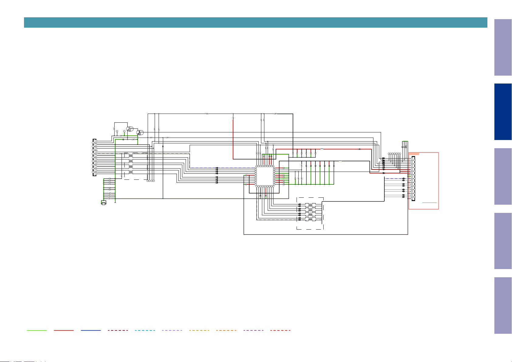
SCH14_FRONT_HDMI
FRO NT_ H D MI PART
Before Servicing
This Unit
Electrical Mechanical Repair Information Updating
R8126 2k
R8127 2k
R8118 0
R8117 0
0.1uF
R8120 0
R8119 O PEN
C8120
R8121 0
SDA_I N
SCL_IN
1
IN0
2
AVEE
IP0
CEC_IN
VREF_I N
3
SCL_O UT
IN1
4
IP1
IC811
5
VTTI
AD8195AC PZ
6
IN2
7
IP2
8
IN3
9
IP3
10
OP1
ON1
AVCC
AVCC
11 12 13 14 15 16 17 1 8 1 9 2 0
ON0
OP0
VTTO
0.1uF
C8111
C8110
R8128
0
OPEN
C8136 OPEN
C8135 OPEN
D8102
T8108
T8109
T8110
T8111
T8112
T8113
T8114
CN811
1
CEC
2
HPD _A
3
TXE N
4
DDCA_ SDA
5
DDCA_ SCL
6
RXA _5V
7
CEC5 V
8
CEC3 .3V
9
CEC3 .3V
10
DGND
11
RXA _C-
RXA _C+
RXA _0-
RXA _0+
RXA _1-
RXA _1+
RXA _2-
RXA _2+
DGND
12
RXA _C-
13
RXA _C+
14
DGND
1517
RXA _0-
1618
RXA _0+
DGND
RXA _1-
19
RXA _1+
20
DGND
RXA _2-
22
RXA _2+
23 21
DGND
CN811
CJP23GA 333ZR
04-6232-023-010-801+
TO DIGIT A L
TO CN710
CEC 3.3V
D8103
KDR720E 30V(1608)
RX_C RX_C +
RX_0RX_0+
RX_1RX_1+
RX_2RX_2+
L8101
CEC 5V
OPEN
R8116
0.1uF
C8119
0.1uF
C8118
AMUXVCC
CEC_O UT
VREF_O UT
3132333435363 7383940
30
AVCC
29
PE_EN
28
SDA_O UT
TX_EN
27
AVEE
26
AVCC
25
AVCC
24
AVEE
23
AVCC
22
AVCC
21
ON2
COMP
OP2
ON3
OP3
0.1uF
0.1uF
C8121
C8122
10/6.3V
C8117
0.1uF
C8116
0.1uF
C8115
0.1uF
C8114
0.1uF
R8122 OPEN
C8134 0.01uF
C8113
0.1uF
C8112
10/6.3V
RX_2+
RX_2RX_1+
RX_1-
0 X 2
RX_0+
RX_0RX_ C+
RX_ C-
OPEN
OPEN
C8123
C8124
C8125
0.1uF
OPEN
C8127
R8124
10/6.3V
R8123 4k7
L8115
0 X 2
L8116
L8117
0 X 2
L8118
0 X 2
E3/ E1C/ K : 0 X 2
E2 : EXC 24CH900U
CB03YT YH 600
OPEN
OPEN
C8126
C8128
C8129
OPEN
OPEN
RX_2+
RX_2-
1234
RX_1+
RX_1-
1234
RX_0+
RX_0-
1234
RX_C+
RX_C-
1234
C8130
C8131
C8132
OPEN
OPEN
FRONT _TM DS
OPEN
L8102
CB03YT YH 600
C8133
R8109
OPEN
Q8101
HVT KRA102S
T8102
22k
C8101
0
.1uF
E3/ E1C/ K : 0 X 2
2k
R8111
E2 : EXC 24CH900U
Q8102
KRC103S
R8104
47k
L8111
0 X 2
1234
L8112
0 X 2
1234
L8113
0 X 2
1234
L8114
0 X 2
1234
47k
OPEN
R8107
R8106
R8105
R8108
0
0
OPEN
D8101
RXF_ CRXF_ C+
RXF_0RXF_0+
RXF_1RXF_1+
RXF_2-
T8103
T8104
T8105
T8106
RXF_2+
1k
T8101
R8102
R8103
19
19.HP DET
18
18.+5 V
17
17.GND
16
16.DDC D ATA
15
15.DDC C LK
14
14.NC
13
13.CEC
12
12.CK-
11
11.D1 SHIE LD
10
10.CK+
9
9.D 0-
8
8.D 1 SH IELD
7.D 0+
6.D 1-
5.D 2 SH IELD
4.D 1+
3.D 2-
2.D 2 SH IELD
1.D 2+
7
6
5
4
CJJ9H021Z
3
2
1
JK811
C8102 0.1uF
C8103 0.1
uF
C8104 0.1uF
C8105 0.1uF
C8106 OPEN
C8107 OPEN
R8112 O PEN
R8113 O PEN
R8114 O PEN
R8115 O PEN
DGND
BK871
DGND
VMC1 A422
(CH GND)
AUX
H DMI_IN PUT
OPEN
R8125
C8108 0. 1uF
C8109
0.1uF
GND LINE
POWER+ LINE
POWER- LINE
ANALOG AUDIO DIGITAL AUDIO
TMDS SIGNAL
ANALOG VIDEO
DIGITAL VIDEO
STBY POWERHDMI
22
Page 23
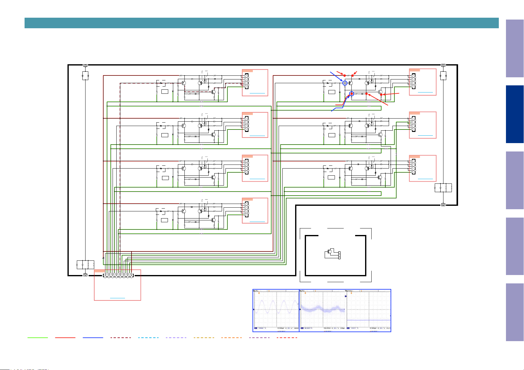
SCH15_DIFF-AMP
AVR-S740H/X1500H DIFF-AM P PART
Before Servicing
This Unit
BK201
CMD1 A569-V
1
PRE_ -B
-56.6V
PRE_ AG ND
J2606
CN55A
13
57
CN56A
13
57
CN57A
13
57
1.FB _FR
2
2.FB _FR
3.PR E_-B
46
4.PR E_-B
5.FR
6.FR
7.AG ND
TO CN55B
CN55A
1.FB _SB L
2
2.FB _SB L
3.PR E_A GND
46
4.PR E_A GND
5.SB L
6.SB L
7.AG ND
TO CN56B
CN56A
1.FB _SB R
2
2.FB _SB R
3.PR E_-B
46
4.PR E_-B
5.SB R
6.SB R
7.AG ND
TO CN57B
CN57A
D2101
Q2102
KSA992F
C2104
2200P
Q2202
KSA992F
C2204
2200P(M)
Q2302
KSA992F
C2304
2200P(M)
Q2402
KSA992F
C2404
2200P(M)
R2108 470K
OPEN
C2106 33pF
R2109 33K
Q2103
KSC1845F
C2105
50V/220uF
(M)
J2101
OPEN
J2104
OPEN
J2201
OPEN
J2204
OPEN
J2301
OPEN
J2304
OPEN
J2401
OPEN
J2404
OPEN
R2111 OP EN
R2110
47(1W)
D2201
OPEN
R2208 470K
C2206 33pF
R2209 33K
Q2203
KSC1845F
C2205
50V/220uF
R2211 OP EN
R2210
47(1W)
D2301
OPEN
R2308 470K
C2306 33pF
R2309 33K
Q2303
KSC1845F
C2305
50V/220uF
R2311 OP EN
R2310
47(1W)
D2401
OPEN
R2408 470K
C2406 33pF
R2409 33K
Q2403
KSC1845F
C2405
50V/220uF
R2411 OP EN
R2410
47(1W)
OPEN
OPEN
C2900
C2901
C2800
50V/47uF
OPEN
OPEN
OPEN
OPEN
J2902
J2901
C2903
C2902
CN201
BK202
CMD1 A387-V1
BK202
123456789
1.FR
3.SR
2.AG ND
FRO M DI GITAL B'D
1.25mm 15P IN B' D TO B'D
FL_IN
SL_IN
CEN_ IN
SR_IN
CN201
1011121314
15
9.FL
7.SL
5.CE N
13.SBL
11.SBR
4.AG ND
15.+12V
6.AG ND
8.AG ND
10.AGN D
12.AGN D
14.AGN D
*O PTIO N
C2101
50V/47uF
100K
R2101
*O PTIO N
C2201
50V/47uF
100K
R2201
*O PTIO N
C2301
50V/47uF
100K
R2301
*O PTIO N
C240
50V/47uF
100K
R2401
R2103
10K
R2102
680
FL
R2202
680
SL
R2302
680
CEN
1
R2402
680
SR
C2103 82pF
Q2101
KSA992F
18K
R2104
C2102
R2107
100V/470pF( M)
220
R2106
R2105 1. 2K
1.2K( 1W)
R2203
10K
C2203 82pF
Q2201
KSA992F
18K
R2204
C2202
R2207
100V/470pF( M)
220
R2205 1.2K
R2206
1.2K( 1W)
R2303
10K
C2303 82pF
Q2301
KSA992F
18K
R2304
C2302
R2307
100V/470pF( M)
220
R2306
R2305 1.2K
1.2K( 1W)
R2403
10K
C2403 82pF
Q2401
KSA992F
18K
R2404
C2402
R2407
100V/470pF( M)
220
R2406
R2405 1.2K
1.2K( 1W)
CN51A
13
57
CN52A
13
57
CN53A
13
57
CN54A
13
57
2
46
CN51A
2
46
CN52A
2
46
CN53A
2
46
CN54A
1.FB _FL
2.FB _FL
3.PR E_-B
4.PR E_-B
5.FL
6.FL
7.AG ND
TO CN51B
1.FB _SL
2.FB _SL
3.PR E_-B
4.PR E_-B
5.SL
6.SL
7.AG ND
TO CN52B
1.FB _CE N
2.FB _CE N
3.PR E_-B
4.PR E_-B
5.CE N
6.CE N
7.AG ND
TO CN53B
1.FB _SR
2.FB _SR
3.PR E_-B
4.PR E_-B
5.SR
6.SR
7.AG ND
TO CN54B
FL O UT
TO MAIN B' D
SL OUT
TO MAIN B' D
CEN OUT
TO MAIN B' D
SR OUT
TO MAIN B' D
FR_IN
SBL_ IN
SBR_ IN
Point A Point B
TO CN822
12V 0.6V
Point A
*O PTIO N
R2501
C2501
50V/47uF
100K
R2503
10K
R2502
680
18K
R2504
FR
C2502
100V/470pF( M)
R2506
R2505 1.2K
1.2K( 1W)
-56.1V
Point B
*O PTIO N
C2601
50V/47uF
100K
R2601
*O PTIO N
C2701
50V/47uF
100K
R2701
R2603
10K
R2602
680
18K
R2604
SB L
C2602
100V/470pF( M)
R2606
R2605 1.2K
1.2K( 1W)
R2703
10K
R2702
680
18K
R2704
SB R
C2702
100V/470pF( M)
R2706
R2705 1.2K
1.2K( 1W)
BIAS TR PAR T
Q2104
KTC3964
(3P,2 MM,50MM,#24)
3.E
2.C
1 2 3
1.B
BN51A
TO MAIN B' D
SAM E B LOCK * 7
C2503 82pF
Q2501
KSA992F
R2507
220
C2603 82pF
Q2601
KSA992F
R2607
220
C2703 82pF
Q2701
KSA992F
R2707
220
Q2502
KSA992F
C2504
2200P(M)
Q2602
KSA992F
C2604
2200P(M)
Q2702
KSA992F
C2704
2200P(M)
D2501
R2508 470K
OPEN
C2506 33pF
R2509 33K
Q2503
KSC1845F
C2505
50V/220uF
R2511 OP EN
R2510
47(1W)
J2501
OPEN
J2504
OPEN
-56.8V
D2601
OPEN
R2608 470K
C2606
33pF
R2609 33K
Q2603
KSC1845F
C2605
50V/220uF
R2611 OP EN
R2610
47(1W)
J2601
OPEN
J2604
J2605
OPEN
OPEN
D2701
OPEN
R2708 470K
C2706 33pF
R2709 33K
Q2703
KSC1845F
C2705
50V/220uF
R2711 OPEN
R2710
47(1W)
J2701
OPEN
J2704
OPEN
Measurement condition
・Voltage measurement
No signal
・Waveform measurement
INPUT: 200mVrms / 1KHz (ANALOG)
Surround mode: MCh Stereo
VOL: 70
Speaker load: 8ohms
BK203
CMD1 A569-V1
OPEN
OPEN
C2904
C2905
FR O UT
TO MAIN B' D
Electrical Mechanical Repair Information Updating
SB L OUT
TO MAIN B' D
SB R OUT
TO MAIN B' D
OPEN
OPEN
OPEN
OPEN
J2903
J2904
C2907
C2906
BK204
CMD1 A387-V1
GND LINE
POWER+ LINE
POWER- LINE
ANALOG AUDIO DIGITAL AUDIO
TMDS SIGNAL
ANALOG VIDEO
DIGITAL VIDEO
STBY POWERHDMI
23
Page 24
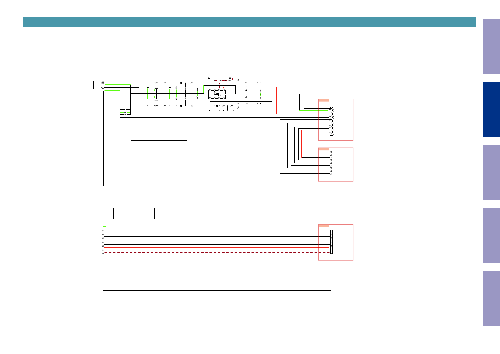
SCH16_PHONO & TUNER
CJJ4N122ZD
L CH
PHONO
R CH
IN
PHONO B'D
JK831
1
2
3
4
5
R8303
R8301
390
0
OPEN
C8301
L8301
OPEN
C8303 220P
220P
OPEN
OPEN
C8302
L8302
C8304
R8304
390
C8319
R8323 0
R8324 0
OPEN
R8302
0
BK801:OPEN
FOR CORSSTALK NOISE(PREPAIR)
Before Servicing
This Unit
C8311
C8313
100V/0.022uF
R8313
C8309
100P
-
B-INPUT
B
B+INPUT
+
V-
A+INPUT
A-INPUT
4 3 2 1
C8310
100P
100V/0.022uF
100V/6800pF
R8315
22
130k
+
-
R8317
11k
8765
V+
B OUTPUT
IC831
A
A OUTPUT
NJM2068MDTE1
R8314
R8316
130k
11k
R8318
C8312
C8314
100V/6800pF
C8315
R8319
47
10/50V
C8317
10/50V
470k
R8321
470k
C8318
10/50V
R8322
R8320
C8316
47
10/50V
22
CN825
_BN826
CN825
C125Z1-15
BN826
15
14
13
12
11
10
9
8
7
6
5
4
3
2
1
9 8 7 6 5 4 3 2 1
15.PHONO_L
14.AGND
13.PHONO_R
12.+7.5V
11.-7.5V
10.CH_GND
9.CH_GND
8.INT
7./RST
6./CE
5.SDIO
4.SCLK
TO DIGITAL B'D
3.VCC
2.TUNER-R
1.TUNER-L
TO CN821
1.L-OUT
2.R-OUT
3.VCC
4.SCLK
5.SDIO
6./CE
7./RST
8.INT
FROM TUNER B'D
9.CH_GND
TO BN826-1
9PIN B'D TO B'D
9PIN B'D TO B'D
Electrical Mechanical Repair Information Updating
C8307
C8305
10/50V
68k
R8305
150k
R8307
150k
68k
R8308
R8306
C8306
10/50V
220/10V
R8309
47
240
R8311
240
R8312
R8310
47
C8308
220/10V
GND LINE
POWER+ LINE
POWER- LINE
TUNER B'D
*TUNER MODULE OPTION
AVR-S740H/X1500H/S640H E3
AVR-X1500H E2
AVR-X1500H E1C
AVR-X1500H K
CHASSIS
CH_GND
8.INT
87654321
7./RST
6./CE
5.SDIO
4.SCLK
TU800
3.VCC
YST990-A9U2
2.R-OUT
1.L-OUT
TUNER MODULE
ANALOG AUDIO DIGITAL AUDIO
CNVYST990-A9U2
CNVYST990-D8E3
CNVYST990-A2J1
CNVYST990-A9U2
TMDS SIGNAL
ANALOG VIDEO
DIGITAL VIDEO
24
BN826-1
BN826-1
987654321
9.CH_GND
8.INT
7./RST
6./CE
5.SDIO
4.SCLK
3.VCC
TO PHONO B'D
2.R-OUT
9PIN B'D TO B'D
1.L-OUT
TO _BN826
STBY POWERHDMI
Page 25
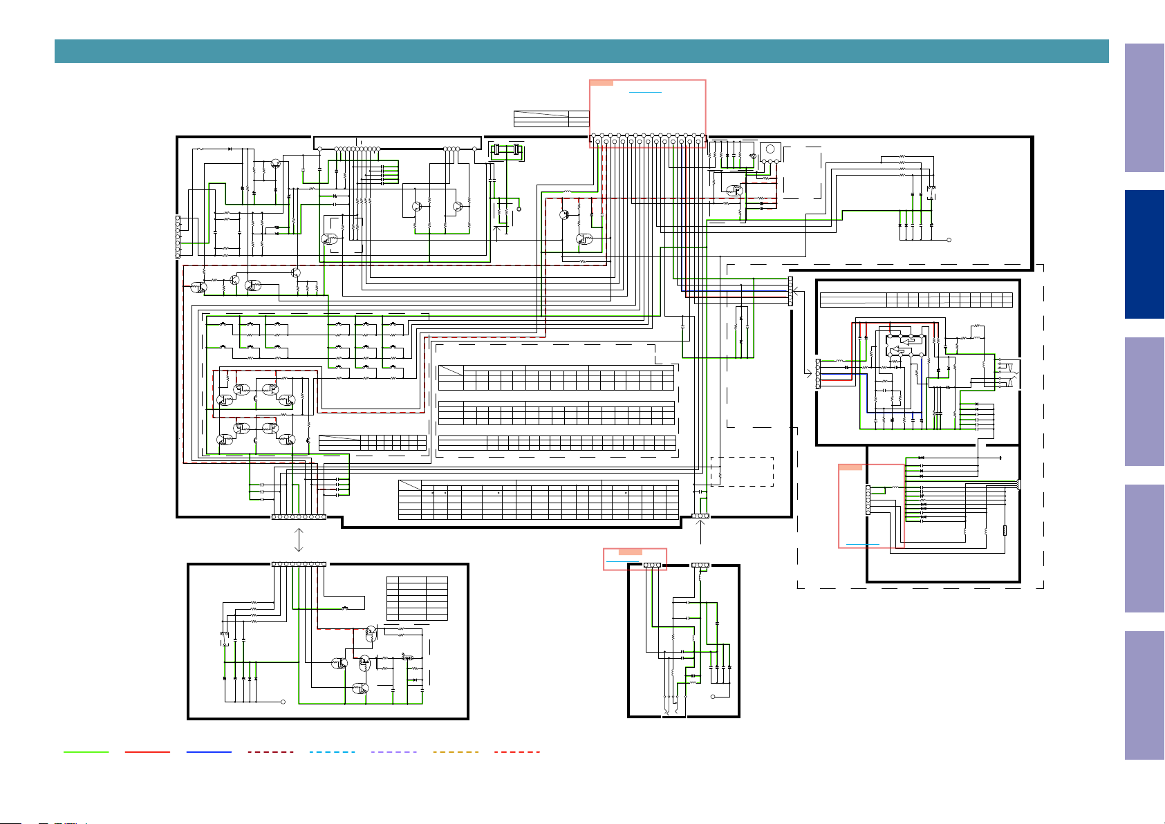
SCH17_FRONT
7. FL _AC
6. NC
5. FL _AC
4. NC
3. GND
FRO M TR ANS
2. NC
1. V DISP
2.5 mm 7PIN WAF ER
FRONT P A RT
F1001
D1001
T 200mA L 250V
1N4007SL
R1001
1.8(A XIAL )
R1002
OPEN (AXIA L)
OPEN
C1001
R1003
OPEN (AXIA L)
1 2 3 4 5 6 7
R1004
CN102
CJP07GB 03ZY
1.8(A XIAL )
2SC3052
Q1016
220K
R1428
R1429
Q1015
10K
R1430
KRC104S
SW102
SW108
R1091
RED_ LED
W/G_ LED
Q1017
KRC102S
Q1021
KRC102S
CUP 12957Z-3
AB
VR102
CSR2A 060Z
C
12CL ICK
EN CO DE R
FU NCTIO N
(SMALL)
22K
OPEN
C1429
EN
OP
0.01uF
C1426
OPEN
C1428
C1002
Q1018
KRA102S
Q1022
KRA102S
100uF/63V
C1005
100V/0.1 uF
SW103
R1071
SW109
R1076
R1413
R1414
R1415
R1416
0.01uF
C1425
OPEN
C1427
KTC1027Y T
R1007
R1062
10K(AX IAL)
27K(1/ 4W)
C1006
50V/1u F
R1424
220
220
R1006
R1009
220
220
R1005
R1008
Q1013
KRC102S
OPEN
OPEN
Q1019
KRA102S
SW115
Q1023
KRA102S
SW116
OPEN
C1087
OPEN
C1086
OPEN
C1085
BN101_1
BN101
10K
10K
1K
1K
OPEN
OPEN
D1406
D1407
OPEN
2.0 mm 9PIN WIRE
2.0 mm 9PIN WIRE
FL101
CFL18BT 021GINK
Q1001
C1007
C1423
OPEN
R1030
Z39V
10(AXIA L)
D1005
C1004
50V/1u F
C1003
R1423
10/50V
47K(AX IAL)
(SMALL)
D1003
Z6.8V
Q1014
KTC1027Y T
1W/10
1W/10
R1427
R1425
R1426
SW104
R1072
OPEN
SW110
R1077
150
R1090
OPEN
Q1020
180
R1082
KRC102S
R1092
OPEN
OPEN
R1081
Q1024
SW114
KRC102S
2. ISE L_A
3. ISE L_B
1. +3 V3
4. DGND
5. DGND
7. RED _LE D
LUG1 4
CHASSI S
8. MC U+5
4. DGND
5. DGND
2. ISE L_A
3. ISE L_B
8. MC U+5
7.RED _LED
6. W/ G_LE D 6. W/ G_LE D
OPEN
1 2 3 4 5 6 7 8 9
1 2 3 4 5 6 7 8 9
1. +3 V3
EN CO D ER &P OW E R
F2
NP
C1009
100V/0.047u F
C1010
(SMALL)
C1011
Q1002
KRC102S
OPEN
SW105
R1073
SW111
R1078
SW117
R1083
TR OPT ION
AVR-S640H/ AVR- S740H/A VR-X 1500H
C1088
C1089
C1090
C1091
9. PO WER_ KEY
9. PO WER_ KEY
ON/ STAN DBY
KRC102S
VFL
GND
0.1uF /50V
47/16V
0.1uF
R1068
150
100
150
OTHER
OPEN
OPEN
OPEN
OPEN
SW101
Q1009
OSC
VDD
VDDH
10(AXIA L)
R1067
39K
OPEN
R1010
*O PTIO N
KRC102S
CSCPDA
TSA
TSB
RESET
43444546474 84 95051525357
C1012
OPEN
C1013
100P
C1014
100P
C1015
330P
C1016
1000P
100
100
100
100
R1012
R1013
R1014
R1015
AVR-X 250BT
AVR-S 540BT/ X550BT
10K
Q1002 OPE N
R1011 OPE N
R1068 0
R1011
AVR-S 640H/A VR-S740H /X1500H
Q1002 KRC 102S
R1011 10K
R1068 OPE N
SW106 SW 107
R1075
R1074
0
100
SW112
SW113
R1080
R1079
0
0
SW118
SW119
R1085
R1084
0
100
Q1017 Q1018 Q1019 Q1020 Q1021 Q 1022 Q 1023
O O O O O O O O
OPEN OP EN OP EN O PEN
OPEN
D1012
R1041
R1042
R1043
R1044
D1002
R1041
R1042
Q1008
KRA102S
CVDP VBW R5A2 M
R1043
4.7K
R1044
Q1011
OPEN
KRA102S
Q1012
C1054
0.1uF
PCB B RAK ET
BK101
BK102
NX
R1018
2SC3052
Q1003
39K
R1025
R1016
+3V3
KEY1
KEY2
KEY3
Q1024
OPEN OPE N O PEN
KE Y NAME
SW102 SW110 SW 111
ADJUS T
AVR-S 540BT
AVR-X 250BT
-
AVR-X 550BT
AVR-S 740H
PURE
AVR-X 1500H
AVR-S 640H
PURE
LED OPT ION
AVRX 1500H E3
OTH ER
WHIT E/RE D
GREEN/R ED
1K2
1K2
4K7
OPEN
OPEN
1SS133M
OPEN
1.2K
1.2K
D1012
R
W/G
SB-LE D
R1045
OPEN
D1002
1SS133M
C1055
0.1uF
F1
NP
Q18G
17G
18G
Q17G
1 2
15678
3 4
CMD1A572
CMD1A572
OPEN
100V/0.047u F
C1041
100
100K
R1026
*O PTIO N
AV R-S540BT /X550B T/X 250BT R ESIST OR V ALUE
AVR-S 540BT
AVR-X 550BT
AVR-X 250BT
AV R-S740H /X1500H /S640H R ESIST OR V ALU E
AVR-S 640H
AVR-S 740H
KE Y OP TION
AVR-S 540BT/ S740H/S 640H
ADJUS T
-
GAME
--
GAME
1K2
1K2
4K7
C1017
100
R1019
2SC3052
Q1004
39K
R1017
5.6K
OPEN
R1071
330 220 180
OTH ER
OPEN
OTH ER
KEY_ 1 KEY_ 2 KEY_ 3
PRESE T-
TUNE +
STAT US
TUNE -
TUNE +
PRESE T-
STAT US
Z2 ON /OFF
TUNE -
MOD E
OPEN
OPEN
R1086
R1087
100K
CHGND
BRACKE T
Op tion
AVR -X1500H E 2/E1 C/K
ON LY
KEY_ 1
KEY_ 2
KEY_ 3
1.5K
2.7K
3.3K
1K
1.5K
OPEN
R1074
R1073
150
OPEN
150
100
SW102 SW 103 SW104 SW 105 SW106 S W107 SW 108 SW109 SW 110 SW111 S W112 SW 113 SW114 SW 115 SW116 S W117 SW 118 SW119
O
O O O O O O O O O O O O O O O O O
OPEN
OPEN
SW107SW105 SW114SW103 S W104 S W106 SW113SW108 SW116SW115SW112SW109
Q/S_ 1
SOUN D
PRESE T-
-
Q/S_ 1
Z2 ON /OFF
-
PRESE T-
PRESE T-
Q/S_ 1 Q/S_ 4
BN12B1
+3V3
R1079 R1080R1077R1072 R1074 R1075 R1078R1073R1071
1.5K
R1079
Q/S_ 4
Q/S_ 4
R1422
0 0
27PIN
NET_FA CT_ RST
BN12B1
R1021
R1020
N.C
1K
3.3K
Q1006
KRC102S
1K
00
R1080R1077R1072
Q/S_ 4
Q/S_ 4
27
C1019
OPEN
OPEN
R1081
330 220 180
OPEN
Q/S_ 2
Q/S_ 2
Q/S_ 2
1.25mm 27PIN FFC
27.NET_ FACT _RST
26.DGND
25.MCU_3V 3
2426
0.01uF
C1020
50V/10uF
R1082
180
BASS/
TREBLE
-
MUSIC
-
MUSIC
*O PTIO N
AVR-S640H /AV R-S740H /AVR -X1500H
AVR-X250B T/A VR-S540B T/A VR-X 550BT
1 2
3 4
BN10
STY LE PI N
1K
0
R1075 R1078
100
0
O O O
ON/O FF
MOVI E
MOVI E
CJP27GB 286ZN
L1001
CB03YT YH 600
OPEN
Q1005
ISA1530AC 1
R1076
2.7K3.3K5.6K 2.7K3.3K5.6K
OPEN
1.5K
1K
KEY_ 2KEY_1
R1076
330 220
180 150 100
OPEN
150 100
OPEN O PEN OPEN OPEN OPEN OPEN
O O O O O O O
PRESE T+
STAT US
SLEEP
-
TUNE +
Q/S_ 2
PRESE T+
MOD E
STAT US
Q/S_ 2
-
Z2 SE L
TUNE +
STAT US
SLEEP
2.0 mm 3PIN WAF ER
TO BN503
TO CN751
FRO M DI GITAL B'D
22.FL_D ATA
20.FL_C E
24.MCU_5V
21.FL_C LK
18.RC_IN
19.FL_R ST
23.CPU_ POW ER
1921
2325
2022
KEY_ 3KEY _2KEY_ 1
R1084 R1085
R1083R1082R1081
1.5K
1.5K2.7K
1K
KEY_ 3
R1083
150
150 100
TUNE -
SOUN D
DIMMER
PRESE T+
TUNE -
Z2 SE L
DIMMER
PRESE T+
PRESE T+
BAND
CN104
CN104
17.W/G _LED
16318
15.KEY _1
16.RED_ LED
1517
1K
0
R1085R1084
100
0
MOD E
Q/S_ 1
BAND
Q/S_ 1
INFO
TO MAIN
CUP 12957Z-4
3.HP_ LCH
13.KEY _3
14.KEY _2
R1090 R1092
R1090
OPEN
OPEN
2.AGND
Before Servicing
This Unit
1.ISEL _A
4.POW ER_ KEY
6.-12V
9.B/P _IRIN _DE
8.AGND
3.MIC _DET
5.+12V
7.MIC _SIGNAL
2.ISEL _B
11.VSEL _A
12.VSEL _B
10.H/P _DET
1011121314
0
0
00
R1092
OPEN
OPEN
SW119SW 118SW117
DIMMER
Q/S_ 3
DIMMER
Q/S_ 3
DIMMER
1.HP_ RCH
123
CJJ2E041ZD
JK104
2. HP _LCH
AVR X1500H E3 ON LY
12456789
390
R1418
OPEN
R1069
Op tion
RC101
38KHZ
390
47K
OPEN
OPEN
C1430
R1420
D1408
R1419
Q1007
KRA102S
R1022
1K
R1023
(38kHz )
OPEN
Op tion
Vcc
GND
VOUT
AVR-X 250BT
LD101
321
AVR-S 540BT/ X550BT
R1421
47K
Q1007 OPE N
R1022 OPE N
R1023 OPE N
R1069 1K
AVR-S 640H
R1024
OPEN
AVR-S 740H/X 1500H
Q1007 KRA 102S
R1022 1K
R1023 47K
R1069 OPE N
R1053
10
C1038
47/16V
(SMALL)
C1039
100P
+3V3
D_GND
VOL-
VOL+
R1061
10K
10K
R1060
1K
R1059
R1058
1K
A B
0.01uF
0.01uF
VR101
CSR2A 055Z
C
C1077
C1076
VO LU ME
24CL ICK
OPEN
0.1uF
OPEN
OPEN
C1074
C1073
D1015
D1016
EN CO DE R
OPEN
(SMALL)
C1075
LUG1 1
CHASSI S
WIRE
Electrical Mechanical Repair Information Updating
CUP 12957Z-1
1. AGND
12345
BN12A
2. MIC _SIGNA L
3. -12V
4. +12V
5. MIC _DE T
Z5.1V
47K
OPEN
AVR -X250BT
OPEN
R1046
2.DGND
1.DGND
123
CN103
2.0 mm 3PIN WAF ER
2.0 mm 3PIN WIRE
2.DGND
1.DGND
123
L1011
CB03YT YH600
C1084
OPEN
1/50V
1/50V
0.1uF
0.1uF
C1065
C1067
C1068
C1066
LUG1 3
CHASSI S
WIRE
H EAD PHO NE
D1403
C1409
R1410
Z5.1V
D1402
AVR -S540BT /X550BT
ON LY
OPEN
C1082
C1081
Q/S_ 3
0.1uF
-----
Q/S_ 3
3.H/ P_DE T
-
Q/S_ 3
3.H/ P_DE T
BN131
C1424
0.1uF
C1069
OPEN
470
R1057
L1010
C1071
CB03YT YH 600
680P
C1072
680P
C1083
L1012
OPEN
CB03YT YH 600
L1013
CB03YT YH 600
18732
87321
3. HP _RCH
8. DGND
7. DE T
1. AGND
* O PTIO N : R ESIS TO R & CAP VA LUE
AVR-S 540BT/ AVR-X 550H
AVR-S 640H/A VR-S740H /AV R-X1500H
0.1uF
1/50V
C1411
2.0 mm 5PIN WIR E
2.0 mm 5PIN WIR E
BN12B
C1417
L1403
CB03YT YH600
1. AGND
12345
C1452
R1433
2. MIC _SIGNA L
50V/10uF
3. -12V
4. +12V
5. MIC _DE T
CU P12957Z-2
AV R-X250B T N OT US ED
100
BN104
TO DIGI TAL B OAR D
2.0 mm 5PIN USB WI RE
TO CN813
R1401 R1435R1408 R1409 C1408R1407 R1437R1434 C 1450R1436 C1406
R1027
V+
(SMALL)
IC101
NJM4580CG
OPEN
O
R1435
R1436
OPTIO N
R1408
33K
C1408
33P
100
R1409
100K
R1432
C1451
50V/100pF
BN104
CB03YT YH600
5.DGND
4.DGND
3.USB D-
2.USB D+
1 2 3 4 5
1.VBU S
CU P12957Z-5
AV R-X250B T S540B T/X550B T NO T US ED
AV R-S640H /AVR -S740H/ X1500H U SE
4K7
8
1K
R1434
C1450
R1407
C1407
L1404
CM1
33p
10K
100/16V
56K
100
7 6 5
CM2
-
10K
1K
R1027
10K
R1431
(SMALL)
D1008
D1020
D1019
OPEN
820
56K
0
33K
10K
100
10K
+-O
2.2K
OPEN
0.1uF
R1412
R1411
4321
V-
+
100
R1406
C1405
10/50V
(SMALL)
OPEN
R1437
C1402
1/50V
(SMALL)
100K
100P
OPEN
(SMALL)
1/50V
C1406
C1410
C1404
C1403
R1404
0.047uF
CDS3 C05HD MI1
0.1uF
C1053
KDS160
KDS160
OPEN
C1051
0.1uF
C1050
220/10V
C1052
(SMALL)
R1040
2.2K
CDS3 C05HD MI1
D1011
CDS3 C05HD MI1
D1010
OPEN
C1049
CDS3 C05HD MI1
D1009
OPEN
C1048
00OPEN
D1404
D1405
C1413
C1414
C1415
C1416
OPEN
27P
0.1uF
0.047uF
33P 33P
R1054
OPEN
L1401
CB03YT YH 600
MICD ET
1
7
6
L1402
CB03YT YH600
3
MIC
MIC
2
4
5
CJJ2D049ZD
JK105
KDS160
KDS160
OPEN
0.1uF
1000P
OPEN
OPEN
0
OPEN
R1401
100
100K
R1402
C1401
2.2K
Z5.1V
R1405
D1401
100K
R1403
JAC K IN : SW OPEN
CHASSI S
META L PLA TE
JK101
4.DGND
3.DA TA+
1 2 3 4
2.DA TA-
1.VBU S
0
0
L1003
L1005
L1004
iP OD /U SB
CB08YT YH 600
GND LINE
POWER+ LINE
POWER- LINE
AUDIO SIGNAL
DIGITAL AUDIO
TMDS SIGNAL
ANALOG VIDEO
STBY POWER
25
Page 26
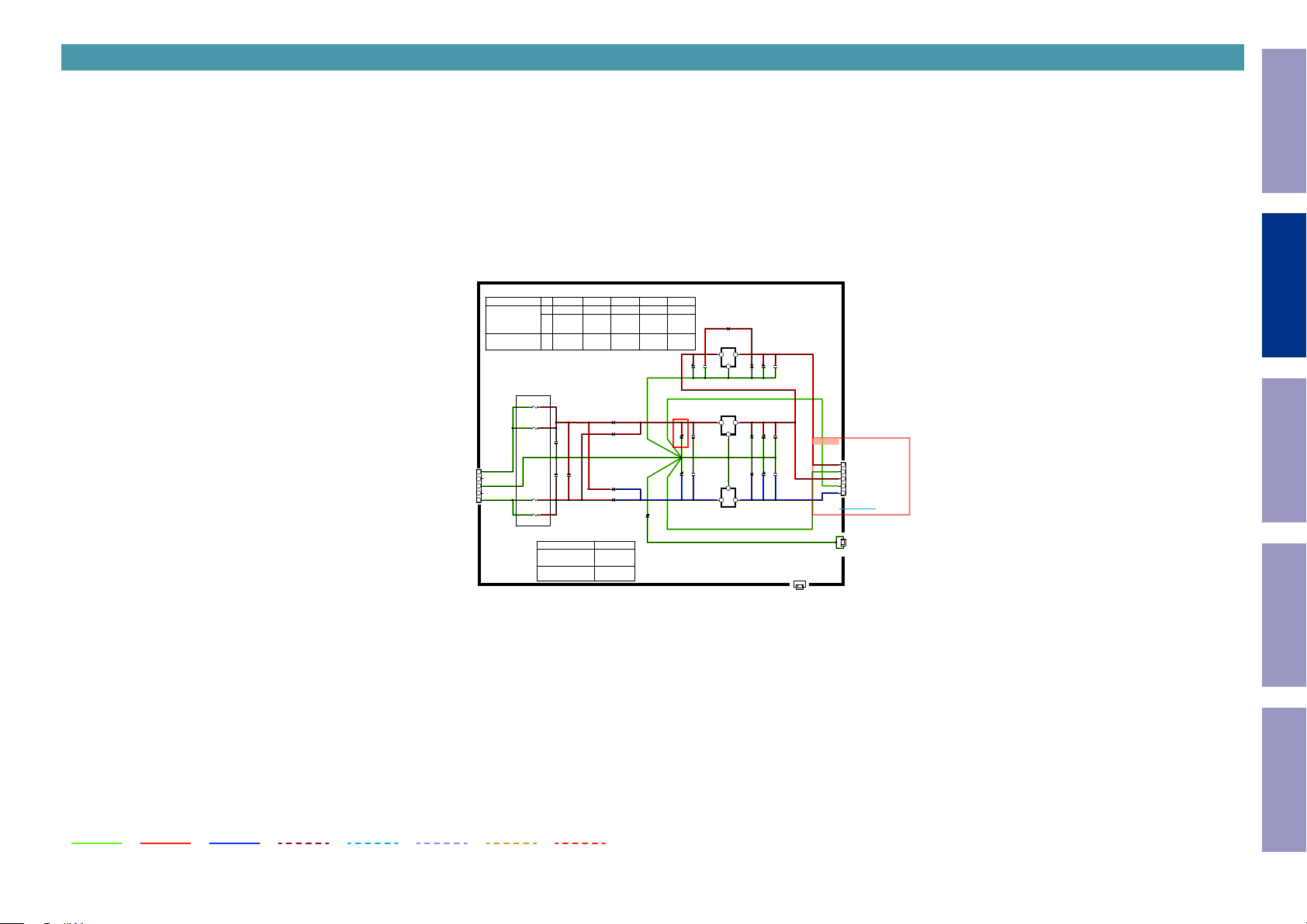
SCH18_REGULATOR
Before Servicing
This Unit
REGULATOR PART
FUS E OP TION
MOD EL
Ver
AC
E3
AC120V
E2
AVR -S740H/ X1500H
AVR -S540BT /S640H
AVR -X250BT /X550B T
AC230V
E1C
AC220V
K
AC100V
ALL
AC120~ 230V
FU SE O PTIO N
F3004
T 1.25A L 250V
F3002
OPEN
OPEN
C3004
CN302
12345
1.AC _S2
2.NC
3.RT N_GND
4.NC
5.AC _S2
FRO M TR ANS
F3001
OPEN
F3003
T 1.25A L 250V
C3003
MOD EL
AVR -S640H
AVR -S740H/ X1500H
AVR -S540BT /X550BT
AVR -X250BT
OPEN
C3005
0.1uF (M)
OPE N O PEN
218Seri es
OPE N O PEN
D3001 UF4004
D3002 UF4004
D3003 UF4004
D3004 UF4004
C3006
25V/6800uF
25V/4700uF
F3002F3001 F3003 F 3004
932Seri es 932Serie s
218Seri es
OPE N O PEN
932Seri es 932Ser ies
OPEN
C3024
Electrical Mechanical Repair Information Updating
D3101
OPEN
IC305
CVIKI A7805BPI
IN
OUT
123
GND
OPEN
C3001
OPEN
C3002
IC301
CVIKI A7812BPI
IN
OUT
123
GND
OPEN
C3006
C3010
4700/25V
OPEN
C3007
C3011
3300/25V
GND
IN
OUT
213
IC302
HVIK IA7912PI
OPEN
OPEN
C3008
C3009
D3108
470/50V
OPEN
C3014
C3012
D3103
470/50V
1SS133MT
C3013
D3104
470/50V
1SS133MT
BN301
BN301
5.D A+5 V
OPEN
C3015
BK303
CMD1 A387
BRAC KET
4.VGND (RE T_GND)
3.+ 12V
2.RL Y_GND
1 2 3 4 5
1.-12V
TO CN823
BK301
CMD1 A569
BRAC KET
TO DIGI TAL B 'D
2mm 5 PIN W IRE
INP UT/V OLU ME PA RT
Bra cke t
No connec tion
GND LINE
POWER+ LINE
POWER- LINE
AUDIO SIGNAL
DIGITAL AUDIO
TMDS SIGNAL
ANALOG VIDEO
STBY POWER
26
Page 27
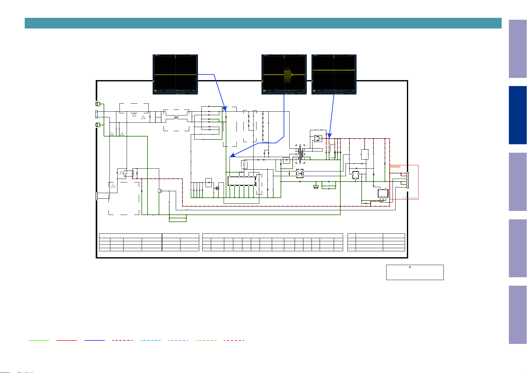
SCH19_SMPS
Before Servicing
This Unit
OP TIO N
CY601
CY602
400V/470pF
!!
!
C6001
250V/0.01u F
!
F6002
AVR -S740H/ X1500H
AC100~ 120V T 6.3A L 250V
AC220~ 230V T 3.15A L 250V
AVR -S540BT /X550BT /X250B T
AVR -S640H
AC120V T 5A L 250V
AC220~ 230V T 2.5A L 250V
OP TIO N
AVR S740H/X 1500H
AC
AC120V
AC220~ 230V
AC100V
AC100~ 120V T 2A L 250V
AC220~ 230V T 1.6A L 250V
F6001
!
400V/470pF
1
324
RY601
HF36FD /5-H LT
F6001 F 6002
2A L 250V
1.6A L 250V
2A L 250V
*O PT ION
8.2M
8.2M
R6027
R6029
!
CX601
0.1uF ,275V
8.2M
8.2M
LF602
R6030
R6028
E3,K :LF-4 ZB-E273H
E2,E 1C:L F-4ZB -E503H
D6009
1SS133MT
C6021
Q6003
50V/0.1 uF
CVT2 SC3052
R6024
10K(1608)
C6022
6.3A L 250V
3.15A L 250V
6.3A L 250V
OPEN
J6014
OPEN
J6015
OPEN
AVR S540BT/ X550BT /X250B T/S640H
F6001 F6002
2A L 250V
1.6A L 250V
-
BK602
BRAC KET
CMD1 A834
12
YAW 396-NNV
CN601
BK601
BRAC KET
CMD1 A834
CN602
YW396-NNB
12
TO POW ER T RANS
OP TIO N
Ver Ver
E3
E1C /E2
K
R6025
4.7K( 1608)
5A L 250V
2.5A L 250V
C6002 250V/0.01u F
D6001 1N 4007
D6002 1N 4007
OPEN
D6003 1N 4007
CX602
D6004 1N 4007
D6005 1N 4007
D6006 1N 4007
J6002
JUMPE R
C6003
250V/0.01u F
1
R603
1M(2125)
R6032
1M(2125)
R6033
1M(2125)
*O PTIO N
OPEN
C6009
50V/0.22u F
C6007 50V/0. 1uF
R6004 330K
C6005
C6006 OPEN
*O PT ION
E1C /E2
-
*O PT ION
*O PT ION
Z22V
ZD611
Z39V
R6008
C6004
200V/100uF
J6003
JUMPE R
Q6002
ZD621
2N7002KA
Z7.5V
D
G
S
R6006
1M(1608)
ZD621
AC
E3
K
AC120V
AC220~ 230V
AC100V
ZJ7.5 B
ZJ16B
ZJ5.6 B
ZD608
Z22V
2.2M( 0.2W )
ZD612
Z39V
ZD609
Z22V
ZD613
C6011
R6009
Z39V
ZD610
Z22V
2.2M( 0.2W )
ZD614
1KV/ 1000pF (S MD)
Z22V
ZD615
Z22V
ZD616
R6010
1M(0 .2W)
Z22V
E3, K:100UF /200V
E1C ,E2 : 100UF/400V
*O PT ION
ZD601
Z12V
4 3 2 1
6
F
D
IC601
CVITO P268VG
S
S S S S S
7
9
8
ZD608 ZD 609 Z D610
ZJ39B
OPE N O PEN OPEN OPEN O PEN OPE N
ZJ39B
ZD617
R6011
10(1608)
C6026
D6012
1N4007
1KV/ 47pF
D6007
ZD618
1N4007
Z27V
270K
R6012
VXC
R6015
R6013
6.8(0 .2W)
22K(1608)
1211
10
AVR S540BT/ X550BT /X250B T, S640H , S740H /X1500H OPT ION L IST
ZJ39B
ZJ39B
*O PTIO N
C6013
C6012
R6014
1K(1608)
47/25V(N XA)
R6008 R6009 R6010 R6012
ZJ39B
2M2 (0.2W )
2M2 (0.2W )
ZJ39B
2M2 (0.2W )
2M2 (0.2W )
C6027
R6034
OPEN
OPEN
OPEN
C6028
1
2
T6001
VLT9 Z132ZW
1
2
3
4
5
D6008
6
)
UF4004
7
C6008
50V/10UF( NXA
Z39V
ZD620
400V/2200pF
0.1uF (1608)
1M( 0.2W )
1M( 0.2W )
3
D6013
RBQ30T 65A
14
J6001
13
OPEN
12
11
10
9
8
12
3 4
IC602
EL817-B
C6023
CMD1A629
BRACKE T
R6013 R6014
270K
22K
56K
22K
270K
22K
BK603
1K
3K
1K
4.7uF (1608)
C6015
C6014 0.1uF(1608)
**OP TIO N
C6024 0.1uF (1608)
R6026
OPEN (1608)
C6025 OPEN (1608)
C6004
100UF/200V
100UF/400V
100UF/200V
100/50V
R6016
56(0.2W )
C6019 5600uF/6.3V (NX A)
C6017
C6018 5600uF/6.3V (NX A)
R6017
R6018
5.6K( 0.2W ) C6020
3.3K( 0.2W )
D6010 OPE N
IC603 K IA2431AP
321
**OP TIO N
Ref N o.
LF602
C6017
E273H
503H
E273H
R6019
22K/F(1608)
0.1uF (1608)
REF
CATHO DE
ANODE
OPEN
R6023
C6029
0.1uF (1608)
AVR S640H/S 740H/X 1500H
100/50V
R6020
OPEN (1608)
6.8K/ F
R6022
CVIPS T8448NR_ A
R6021
OPEN (0.2W )
Z6.8V
ZD619
BN601
OPEN
C6010
C6030
15N(1608)
4
NC
CD
IC604
GND
VDD
OUT
2
1 5
3
AVR S540BT/ X550BT
AVR X250BT
OPE N
** IMPO RTAN T SA FETY NOT ICE.
COMP ONEN T ID ENTIF IED B Y MARK HAV E SPE CIAL CHAR ACT ERISIC S.
IMPOR TAN T FOR SAFE TY. WHE N REP LACING ANY OF TH ESE COMP ONEN TS
USE O NLY MANUFA CTUR ER'S S PECI FIED P ART S.
** THE UNIT OF RE SIST ANCE IS OH M.
K = 1000 O HM. M = 1000KOH M.
** THE UNIT OF C APAC ITAN CE IS MICRO FARA D(u F)
pF = 10 uF
** THIS SCH EMATIC DIAG RAM MAY M ODI FIED A T AN Y TI ME W ITH T HE
IMPRO VEME NT O F PER FORMANC E.
-6
L6001
0
TO CN741
12
D5.2 V
D5.2 V
3456
M_RES ET
DGND
DGND
MAINPOW ER
BN601
TO DIGI TAL B 'D
DIG ITAL POW ER P ART
Electrical Mechanical Repair Information Updating
GND LINE
POWER+ LINE
POWER- LINE
AUDIO SIGNAL
DIGITAL AUDIO
TMDS SIGNAL
ANALOG VIDEO
STBY POWER
27
Page 28
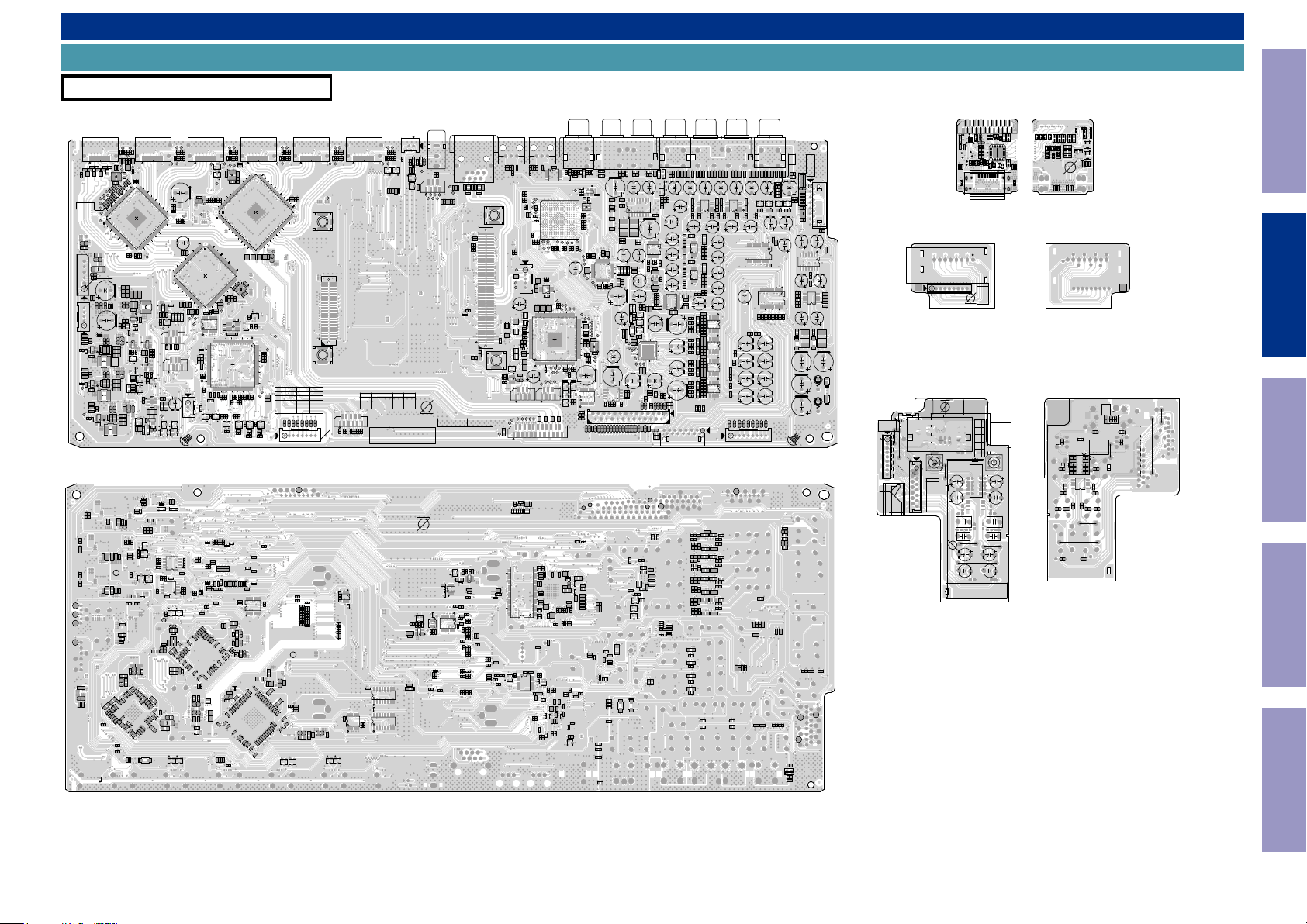
CUP12909Z-4
+12V
BN826
PRINTED CIRCUIT BOARDS
DIGITAL, F HDMI, TUNER, PHONE
Lead-free Solder
When soldering, use the Lead-free Solder (Sn-Ag-Cu).
R7591
Q7594
C7502
R7333
C7183
R7326
R7545
R7592
R7366
R7365
C7314
C7122
C7119
R7147
R7145
R7146
R7144
R7143
109
R7327
R7328
X7501
R7547
R9003
R7503
R7502
C7315
C7118
C7160
C7159
JK721
A
A
54
R7330
C7351
X7301
C7350
R7357
C7354
R7506
10873
R7559
R7558
C7513
R7548
R7546
R7593
Q7595
R7597
R7595
R7596
C7527
R7508
C7517
R7501
IC734
C7328
L7306
L7308
C7338
L7307
L7302
C7127
C7126
C7185
C7125
C7124
C7123
C7121
C7186
C7120
C7158
C7156
C7157
R7142
C7152
+5V_3
162109
R7134
R7133
R7132
RN716RN715RN713
L7107
Q7301
R7358
R7361
CPU_PW
R7549
R7553
R7552
R7261
109 144
CEC_PW
R7581
N3V3_PW
R7582
R7560
R7600
Q7596
C7593C7592
R7598
R7599
R7551
C7514
C7515
C7516
R8186
C7190
C7192
C7130
C7129
C7128
C7175
C7131
C7172
C7132
C7133
C7134
C7168
C7135
C7170
C7136
C7137
C7138
C7169
C7143
C7165
C7145
C7146
C7144
C7147
C7171
C7148
C7149
C7150
C7167
C7151
DA_3
CK_3
B
B
HPD_3
B
B
AVDD11RX
N5V_PW
VER.
X1500H E3
X1500H E2
X1500H E1C
X1500H JP
S740H E3
L7551
CN753
L7104
C7179
C7180
C7178
PVDD33
C7191
C7139
C7166
C7140
C7142
Q7121
R7140
L7552
L7553
+1.1V
R7135
C7141
JK711
R7124
R7123
R7128
R7127
R7122
R7121
R7125
R7126
C7115
R7158
R7157
R7139
10855
R7581 R7582
OPEN
0
10K
10K
18K
L7556
L7554
R8141
R8142
R8144
R8146
R8148
R8150
R8151
R8154
R8157
R8159
787_HINT
R7136
R7137
R7138
L7102
AVDD33RX
Q7122
B
B
+5V_2
R7114
R7113
R7118
R7117
R7112
R7111
R7115
R7116
C7114
VDD33
BK812
41
25
1535
5
BK811
0
OPEN
10K
22K
1.THERMALDET_A
2.RLY_GND
3K3
L7557
L7559
L7558
R8143
R8145
R8147
R8149
R8152
R8153
R8155
R8156
R8158
L7103
C7177
C7176
C7295
C7174
JK751
R8811
R7237
R7236
R7235
5.DA+5V
4.VGND(RET_GND)
3.+12V
2.RLY_GND
1.-12V
CN741
CN823
R7425
C7431
R7421
IN
R7414
R7415
C7418
R7411
D5V_PW
DA_PW2
R7412
R7413
R7422
R7423
-12V
+12V
+5V
+5V
L7206
C7288
CK_5
DA_5
CK_OUT
DA_OUT
+5V_OUT
D7224
D7227
D7223
D7228
D7221
D7222
D7225
D7226
C7276
RN724
RN722RN721 RN723
X7201
R7251
R7249
R7250
R7252
MCK
64FS
FS
I2S3
I2S2
I2S1
I2S0
R7268
R7267
R7266
R7234
R7233
R7232
144
T7239
IC721
T7238
L7208
C7293
C7290
L7210
L7207
6.MAIN_POWER
5.DGND
L7404
4.DGND
R7483
3.M_RESET
2.D5.2V
1.D5.2V
C7401
1 6
C7403
C7402
L7401
51
C7407
C7405
L7403
C7406
L7402
C7408
D1.8V
R7424
C7404
L7421
R7426R7416
L7425
L7422
IC742
C7433
C7424
C7430
C7427
C7429
L7423
L7414
L7412
L7411
C7416
C7415
C7414
IC741
C7411
C7420
C7417
C7421
C7419
R7434
R7435
L7413
C7443
L7432
R7436
R7431
IC743
C7437
C7442
L7433
R7433
R7432
C7438
C7449
C7423
C7413
C7422
C7412
C7436
C7426
C7435
C7425
C7285
L7204
C7294
C7237
C7236
C7289
R7221
R7265
R7264
C7270
C7269
C7287
R7238
R7243
R7244
D7229
19191919 1919
JK741
HPD_OUT
ARC
+5V_5
HPD_5
D7230
D7231
R7254
R7253
R7257
R7256
788_RST
D7233
RN725
R7258
R7260
R7259
C7275
C7274
C7273
R7229
R7230
C7271
R7231
R7228
R7227
37 72
C7239
C7238
R7223
C7457
C7458
C7459
IC744
C7455
C7450
R7441
Q7417
R7478
R7468
C7473
R7494
L7801
L7434
Q7420
R7487
C7484
R7486
R7489
C7485
+1.1V
R7497
R7481
R7480
C7173
L7201
L7202
C7280
C7231
C7230
C7229
C7228
D7232
C7281
R7219
R7220
R7262
R7263
73 108
R7226
R7225
HAINT
36
37 72
L7443
C7472
Q7408
D7237
D7236
D7235
C7471
R7464
R7463
R7462
Q7407
276
CN731
DV_PW
5
Q7413
R7351
R7350
R7470
R7471
CN721
276
R7473
R7353
R7352
C7475
R7469
C7474
Q7410
5
R7467
R7466
Q7409
R7465
Q7503 Q7502
C7490
IC747
R7498
C7489
C7488
C7486
CEC_PW2
IC746
C7482
Q7424
Q7422
C7481
L7451
Q7423 Q7421
D7401
D7402
R7485
R7492
R7493
R7490
C7483
R7484
R7491
D7404
D7403
C7487
R7495
R7496
Q7419
Q7418
R7271
R7273
R7274
C7297
R7363
R7362
Q7411
IC723
R7364
R7344
Q7412
R7346
C7476
IC732
C7352
R7275
Q7221
+1.8V
L7305
C7326
C7319
C7318
C7322
L7304
C7317
C7311
L7303
C7310
C7308
C7306
C7279 C7277
C7313
C7316
L7301
C7241
C7242
C7243
C7283
C7244
C7291
C7247
C7248
C7245
C7249
C7246
L7209
C7254
L7203
C7255
C7256
C7257
C7258
C7282
C7292
C7259
C7260
C7261
C7262
Q7212
Q7211
D7238
C7272
R7248
R7222
R7224
CEC1V1
L7441
L7442
R7444
C7432
C7428
L7431
C7441
C7447
+3.3V
R7427R7417
C7222
C7221
L7205
109
R7247
36
R7449
R7448
R7447
C7453
C7452
C7454
R7446
C7456
R7445
C7480
L7424
R7479
C7479
C7434
Q7416
Q7501
L7415
D3.3V
R7571
R7572
R7573
R7575
C7521
D7502
R7574
D1.0V
R7437
C7446
C7445
C7440
C7439
C7444
R7488
C7448
R7576
R7577
C7522
R7578
R7569
R7570
C7520
R7477
R7443R7442
C7451
C7462
C7460
C7461
C7278
C7284
C7240
C7227
C7226
C7225
C7224
C7223
C7268
C7286
C7267
C7266
C7265
C7264
C7263
R7255
R7246
R7245
R7360
R7309
R7307
R7308
3.D5V
2.HI-B_RLY
1.DGND
Q7222
C7325
R7303
C7321
R7302
C7312
JK731
R7217
R7211
C7211
VDD11
788_HINT
C7309
R7359
R7334
R7306
R7314
R7312
R7311
R7310
D7234
OSD_CS
OSD_CLK
IC722
R9001
ADV7623_ROM
C7509
R7521
R7522
R7528
MN864788_ROM
R7529
R7272
R7270
R7269
R7343
R7345
R7342
R7279
R7282
R7316
R7315
C7324
C7323
R7341
R7340
R7305
R7304
C7307
C7305
C7304
C7301
C7194
C7193
L7108
L7109
C7195
R7218
R7214
R7213
R7212
R7216
R7215
C7188
L7106
VDD33IO
IC731
R7313
OSD_MO
OSD_MI
R7523
T1
R7530
CN756
C7594
Q7591
R7527
R7526
R7513
R7512
R7278
R7281
C7329
R7318
R7317
C7303
C7302
R7301
AVDD11TX
C7196
C7189
HPD_4
R7207
C7201
C7296
2011
7237
R7531
R7525
R7524
R7515
R7514
R7511
Q7201
R7208
R7204
R7203
Q7202
R7202
R7201
R7206
R7205
P_DA
R7152
R7150
R7155
R7153
R7151
R7131
R7156
216163
IC701
144
73 108
R7320
R7319
C7506
10
36
IC751
C7511
R7533
C7501
R7536
R7541
R7586
R7587
Q7592
Q7593
R7539
R7538
R7537
R7535
R7534
C7510
R7518
R7517
R7356
C7508
R7510
R7509
R7583
R7277
R7280
R7283
R7349
R7348
C7330
C7331
C7332
C7333
C7327
C7334
C7336
C7337
C7346
R7335
C7345
C7347
C7348
C7349
RN714
C7181
RN712RN711
C7164
C7187
R7149
R7154
R7148
C7155
DA_4
CK_4
A
A
+5V_4
P_CK
787_RST
C7153
X7101
C7154
R7329
C7335
A_CK
A_RST
R7324
R7323
A_DA
R7322
R7321
C7505
R7505
R7544
R9002
R7542
R7540
R7590
R7589
C7591
R7588
R7594
R7543
C7512
R7520
R7519
C7503
C7504
R7504
C7507
R7584
C7342
C7341
C7340
R7331
R7332
C7343
C7344
C7184
AVDD33TX
C7182
L7105
C7117
C7116
C7163
C7162
C7161
DA_2
C
C
HPD_2
3.H/P_RLY
R8139
R8161
R8160
R8163
R8162
R8165
R8164
R8167
R8166
CK_2
4030
20
10
2
CN812
6.FRONT_RLY
4.HI-B_RLY
5.+12V
CN752
2
R7561
R7568
R7567
R8140
C7353
Q7112 Q7111
JK701
8.SB_RLY
7.C/S_RLY
10
11
R7565
R7564
R7563
R7499
R7566
R7562
IC813
C8109
R7354
IC733
MI ICT FCT1 FCT2
MCU_E20/EMULATOR
C7518
R7355
DIGITAL (A SIDE)
1 3
DA_1
CK_1
CN755
4 2
D9002
C9001
R7585
HPD_1
R9004
+5V_1
Q7102
R9005
R9006
Q7101
CN771
Q9001
R7104
R7103
R7108
R7107
R9007
R7102
R7101
R7105
R7106
Q9002
C7113
PLD_EMULATOR
C8121
R8183
R8184
R8185
TH801
RP
MP_CUP12958Z_A
BAR CODE LABEL
DIGITAL (A SIDE)
R7457
R7456
R7454
C7468
C7467
R7579
D7501
IC752
C7519
IC753
D9001
L9001
T225
2
J_TDO
J_TCK
DGND
Pb
PbPb
PbPb
R8178
Q7403
C7466
T90
R8179
Q7404
R8021
1
2
3
JK901
R7747
R7746
T20
R8181
T326
765
C8118
PLD_WRITE
J_TMS
R8132
R8138
R8135
R8133
R8136
R8131
J_TDI
DA3V3
VERSION
24.MCU+5V
27.DGND
23.CPU_POWER
25.MCU_3V3
26.DGND
21.FL_CLK
22.FL_DATA
Q7401
C7465
C8107
R8101
R8001
IC811
T91
R8004
C8108
IC815
IC812
C8116
R8180
R8011
R8012
R8013
R8015
R8023
7
8 2
D8103
L8103
C8117
C8119 C8120
R8022
R8020
R8018
R8003
R8002
R8174
14.KEY_2
15.KEY_1
16.RED_LED
17.GRN_LED
19.FL_RST
18.RC_IN
20.FL_CE
R7453
R7452
R7451
C7463
Q7402
C7464
R8102
R8104
R8105
R8107
R8006
R8005
R8112
R8113
R8114
R8115
R8172
R8120
R8119
R8125
R8127
R8130
R8137
R8134
R8129
D8104
13.KEY_3
D8101
R8025
R8024
45556575
35 15
25
5
11.VSEL_A
12.VSEL_B
C8103
C8106C8105
R8106
R8108
R8109
R8110
R8111
R8171
R8116
R8168
R8170
R8169
R8124
1
R8175
9.B/P_IRIN_DE
10.H/P_DET
R8009
L8104
CN811
8.MIC_GND
R8007
R8008
R8016
R8126
R8128
BK814
JK811
D8102
60 70 80
30 40 50
20
10
2
R7475
5.+12V
7.MIC_SIGNAL
6.-12V
4.POWER_KEY
C8104
C8102
R8103
JK762
C7844
C7845
C7842
C7843
R7474
R7476
CEC
3.MIC_DET
2.ISEL_B
R8117
R8118
R8121
R8123 R8122
R8019
C7477
1.ISEL_A
R8014
R7622
BK813
C8101
DSP_DEBUG
D7131
R8010
R8017
R7624
R7623
R7777
L8102
RN811
T223
T222
RN794
RN793
C7825
C7826
R7838
C7827
R7839
R7840
R7841
RN790 RN789
Q7414
Q7415
CN782
TXEN
HPD_F
R7109
C7111
Q7701
JK761
R7625
C7617
C7616
C7619
R7626
R7627
C7618
R7629
R7628
7
R7707
R7703
AP_CK
AP_DA
R7706
R7702R7701
A
B
R7704
C
R7709
AP_CS
D
E
F
PLD_ERR
R7705
R7714
G
R7715
H
J
K
R7720
L
M
N
P
R
T
R7728
J_TDI1
R7729
R7732
R7739
R7778
J_TCK1
T224
C8111
C8110
51
85
R8182
C8112
CN813
RN785
RN787 RN786
RN791
RN788
C7808
109
C7823
C7824
C7828
C7829
144
RN781
IC781
RN782
R7804
C7807
C7478
DI_SB/SR
DI_-/SW
L7802
2765276
T7804
T7803
T7802
T7801
DSP_ROM
CEC3V
DA_F
CEC5V
+5V_F
CK_F
RN702
RN701
251015202322
C7103
C7101
C7102
C7112
L7101
C7110
C7106
C7107
C7109
C7108
C7105
C7104
R7803
C7841
C7840
C7801
R7802
R7801
C7821
IC784
C7834
C7835
C7833
C7832
C8113
R8173
R7745
R7779
R7780
C7759
R7782
R7776
RN771
C7705
IC772
R7744
R7721
C7721
R7718
R7716
R7717
C7702
C7703
R7713
R7708
Before Servicing
This Unit
F HDMI (A SIDE) F HDMI (B SIDE)
251015202322
T8114
T8109
T8113
T8112
R8123
L8102
T8111
D8101
CUP12959Z-2_MP
JK104
L8302
C1065
CN825
CN825
1.TUNER-L
2.TUNER-R
3.VCC
4.SCLK
5.SDIO
6./CE
7./RST
8.INT
9.CH_GND
10.CH_GND
11.-7.5V
12.+7.5V
15 111
13.PHONO_R
14.AGND
15.PHONO_L
BN826-1
MP STAGE
5 4
BK801
Pb
Pb
3287
J106
C8306
Pb
T8108
L8101
R8116
D8103
R8127
R8126
T8110
R8128
R8117
T8102
R8118
R8125
T8104
4031
R8119
T8105
T8106
T8103
T8101
C8103
C8102
R8120
R8111
C8101
R8121
R8104
R8107
R8106
JK811
19
C8106
BK871
1 8
BN826-1
9.CH_GND
8.INT
7./RST
6./CE
9
5.SDIO
4.SCLK
3.VCC
Pb
2.R-OUT
1.L-OUT
2
MI RPFCT2FCT1ICTMI RPFCT2FCT1ICT
1
1 3
1.D GND
2.D GND
3.H/P DET
1.D GND
2.D GND
3.H/P DET
VERSION
BN131
C8308
C8312
C8311
C8314
J108
J107
C8318
J104
C8316
135642
1
C9504
2
JK951
14
C8826
R9506
8
R9507
IC951
C9503
R9508
DA_PW
IC771
T11
T13
J_TMS1
T9T7
J_TDO1
R7727
R7730
R7734
R7733
R7731
R7740
R7737
C7602
R8177
C8115
4
IC814
T7807
R7859
D_MISO
D_FLG0
R7860
D_CK
D_BSY
D_RST
R7806
R7805
R7867
R7869
DI_CSW/C
DI_BCK
DI_S/SL
DI_-/FR
R7809
CN781
5
Q7805
Q7804
R7866
Q7803
R7868
L7501
RN703
RN704
CN710
C7805
C7804
R7807
C7803
C7802
R7865
R7864
R7863
C7809
C7810
L7803
C7813
C7812
C7838
C7839
C7837
C7817
R7837
R7836
R7858
C7820
C7836
RN792
C7819
RN784
R7835
R7870
R7857
R7856
R7855
R7736
R7735
R7748
R7738
C7701
C7711
C7710 C7709
C7707
C7708
C7720
C7716
C7719
C7712
C7717
C7718
C7706
C7704
C7715
C7713
R7458
R7711
R7710
Q7405
R8803
C8803
C8812
C9501
R9502
R9501
R9505
R9504
C9502
R9503
D9501
Q7406
C7469
R7460
R7459
C7470
16151413121110987654321
C8801
R7781
C7722
C8821
X7701
C8804
R7719
R7722
R8806
R7723
C8825
R7724
R7726
C8822
R7725
C7998
T15
C7987
R7742
R7601
RN761
256FSDIR1
R7606
R7605
R7604
64FSDIR1
FSDIR1
12
R7603
IC761
DATADIR1
13 24
RN762
D7601
37 48
DR_DIN
DR_DOUT
25 36
C7609
DR_CK
DR_CE
R7613
R7610
R7609
R7612
R7611
C7603
D_MOSI
D_CS
C7615
73 108
DI_MCK
DO_EXT2
DO_EXT1
R7862
C8259
DO_SB
DO_S
DO_C
DO_LRCK
DO_BCK
DO_F
RN783 RN795
R7861
C7815
R7822
DA256FS1
C7936
X7801
R7821
R7823
C7814
R7819
DI_LRCK
37 72
DI_F/FL
R7817
C7806
R7816
36
R7815
R7814
R7813
R7812
C7930
2011
IC783
Q7802
5 8
IC782
Q7801
C7830
R7849
R7847
10
CN751
R7848
C7526
L7503
L7504
L7502
L7512
L7511
L7510
L7509
L7508
L7507
L7506
L7505
C7525
+5V
+3.3V
R7871
C7831
C7846
R7820
R7818
C7816C7811
R7832
R7824
R7831
R7829
R7830
R7827
C7818
R7828
R7825
R7826
R7833
C7601
C7608
C7604
R7614
R7607
R7608
R7602
R7621
R7743
C7714
C8829
D8801
C8802
C8828
C7822
C8820
C8823
C8824
C8827
R8808
1
JK881
JK822
C8805
5
C8806
C8807
R8804
D8504
C8265
R8802
R8801
R8265
C8809
C8810
R8805
IC881
C7614
D7603
D7602
R7617
R8256
D8209
D8205
R8257
D8206
R8255
DAFS1
DADATAF1
DA64FS1
DA_Z_MUTE1
C7928
4
R7842
L7515
L7514
L7513
R7902
Q9102
Q9103
C7610
C7611
C7613
D8802
169
R8807
C7642
C7643
C7612
R7618
R7619
D7604
C7652
C7605
D8204
D8203
R8259
C7935
R7901
12
DA_DA1
R7845
R7846
R7844
R7843
11
L7518
L7517
L7516
C8261
C7995
C7997
R9116
Q9101
C8808
R9117
DA_CK1
L7519
C7996
C7992
C7656
C7655
Q8203
Q8201 Q8202
4837
DA_MS1
C8258
C7986
L7522
C7524
C8264
R8264
C9120
D8503
Q8204
Q8205
R8261
R8263
R8260
R8262
C8262
C8811
8
C8813
C7638
8
IC764
C7639
9 16
C7628
R7647
R7646
C7644
R7662
C7653
R7660
C7654
C7629
IC766
R7661
IC765
R7658
R7657
R7656
R7655
R7652
R7654
2011
D7605
C7648
C7985
C8260
C7916
R8258
IC791
25 36
2413
C7926
C7988
C8257
C7902
R8810
R8809
C7989
R8236
R7580
1 272621
L7525
L7524
L7520
111
15
220 10
L8202
C7523
L7523
12
C8831
C8830
+12V
-12V
+12V
C7994
C7990
R7620
C7925
C7915
C7919
C7927
C7917
C7929
C7993
C7646
C7649
C7650
R7653
R7650
R7651
C7641
C7640
7 52
3
JK821
C8215
R8266
42
R8213
R8215
R8218
C8217
C8216
R8219
R8216
R8217
C8219
R8220
C8220
R8267
C8273
C8274
C8268
C8267
IC824 IC823
R8272
R8281
4854
R8280
R8285
R8276
85
R8284
C8263
R8287
R8286
R8278
R8291
R8290
C8280C8279
C7635
C7634
845
C7637C7627
C7630
R7641
R7639
R7638
C7636
R7643
C7631
R7645
IC763
R7642
C7624
8
5
C7625
C7620
R7630
R7631
C7626
R7635
R7634
4
IC762
R7637 R7633
C7658
R7659
C7621
10
R8246
R8245
C8239
R7649
R7648
C8240
C7657
4
IC795
C7901
C7918
C7920
C7999
L7527
L7526
C7991
14.AGND
15.+12V
14.AGND
15.+12V
C7645
C7647
C7651
C7974
R7972
R7978
R7971
R7977
R7976
R7986
R7982
R7987
R7981
C7981 C7971
R7988
85
4
IC794
C7954
R7952
R7958
R7951
R7956
R7957
R7967
R7962
R7966
R7968
R7961
C7961 C7951
85
4
R7932
IC793
R7931
C7934
R7948
C7931
R7947
R7946
R7937
R7936
C7941
R7938
R7942
85
4
IC792
R7941
R8248R8247
85
R7912
C7914
R7918
R7911
C7911
R7916
R7917
R7922
R7927
R7921
C7921
R7926
R7928
C8254
C8252
C8256
L7561
1.FR
2.AGND
3.SR
1.FR
2.AGND
3.SR
4.AGND
9.FL
4.AGND
9.FL
CN822
5.CEN
6.AGND
7.SL
8.AGND
10.AGND
11.SBR
12.AGND
5.CEN
6.AGND
7.SL
8.AGND
10.AGND
11.SBR
12.AGND
13.SBL
13.SBL
CN754
410
R7925
C8255
R7924
C7924
R7929
R7923
C7922
C7923
R7919
R7915
R7914
R7913
C7913 C7912
C7944
R7935
R7934
R7933
R7949
C7933 C7932
R7939
C7942
R7944
R7945
R7943
C7943
R7963
R7965
C7964
R7964
R7969
C7963 C7962
R7959
R7953
R7955
R7954
C7953
C7952
R7985
R7984
C7984
R7983
R7989
C7983 C7982
R7979
R7973
R7974
R7975
C7973 C7972
C7623
R7636
C7622
R7632
C7633
R7644
C7632
R7640
C8276
C8275
3
1
C8209
R8205
R8271
C9119
R9132
R9127
R9130
Q9107 Q9106
Q9104
R9126
C9114
C8221
9.CHGND
8.TUNER_INT
3217
7.TUNER_RST
6.TUNER_CE
C8222
5.TUNER_SDIO
4.TUNER_SCLK
3.VCC
2.R-OUT
1.L-OUT
CN821
R8227
R8229
R8228
C8251
C8249C8248
C8247
C8245C8244
L7568
L7567
1.CURRENT_DET
91 551 8
C8227
R8235
C8226
R9122
JK911
42
R9131
C9118
R9129
C8207
R9125
R9119
R9118
C9113
IC822
3217
R8232
R8231
R8230
C9105
C8235
C8236
6.DGND
3.-12V
4.MUTE_+B
5.ASO_DET
2.CURRENT_GND
C8234
L8203
C8237
C8238
L8204
L8205
C8233
C8225
R9123
R9121
C8213
C8212
C8210
R8221
C8214
C8211
R8211
R8222
C8203
R8208
C8202
R8207
C9102
7
8 14
R9108
R9110
C9111
85
R9113
C9109 C9108
C9103
D9101
9.AMPSIG_DET
7.DC_PROT
8.THERMALDET_B
-7.5V
+5V
R8212
D8207
D8208
R8270
C8208
R8202
R8201
R8203
L8201
C8206
C8205
C8204
R8209
C8201
CN821
410
111
12
15
R8210
C9101
R9103
OUT
IC911
R9106
R9107
C9107
R9109
4
R9111
C9112
R9114R9112
R9115
IC912
C9110
C9104
R9102R9101
C9106
D9102
R8240
D8201
R8241
D8202
TUNER (A SIDE)
PHONE (A SIDE)
9.CH_GND
8.INT
7./RST
6./CE
4.SCLK
2.R-OUT
5.SDIO
3.VCC
1.L-OUT
BN826
CN104
2.A GND
3.H/P L
1.H/P R
2.A GND
3.H/P L
1.H/P R
J105
J102
J101
C1067
JK831
2 14
LUG13
9
10
R9105
C8243
R9104
+7.5V
3 61 4
5
C8218
R8269
R8268
R8214
R9128
C8266
C9117
C9116
Q9105
R8273
R9120
R8277
R8279
R8289
R8288
C9115
C8278C8277
IC821
16
16
C8229
R8226
R8225
R8254
R8253
C8250
R8252
R8251
C8246
R8250R8249
L7566
L7562
L7565
L7564
L7563
L7560
-12V
C8253
R8244
R8243
C8228
C8223
R8234
C8224
R8233
C8270
R9124
C8269
R8122
C8112
C8129
C8134
R8124
3021
C8109
2011
IC811
10
C8104
C8128
L8114
L8112
L8111
L8113
C8107
BK871
TU800
L8301
C8305
C8307
CUP12959Z-1_MP
C8313
C8317
C8315
BAR CODE LABEL
MP_CUP12833Z_A
C8131
C8133
L8115
L8118
L8117
L8116
CN811
C8127
C8110
C8108
C8117
C8111
C8113
C8121
C8115
C8120
C8118
C8105
C8116
C8119
C8114
R8114
R8112
TUNER (B SIDE)
PHONE (B SIDE)
C1083
R1057
R8309
R8313
R8315
C8136
C8135
C8130
C8126
C8132
D8102
Q8102
C8123
C8124
C8122
Q8101
C8125
R8109
R8103
Pb
R8115
R8113
18
C8301
L1012
C1424
R8301
C1069
L1013
IC831
5 8
C8309
R8320
R8319
R8317
R8322
R8321
R8108
R8105
R8102
2
Pb
13
C1071
R8303
C8303
R8305
R8307
R8311
L1011
C1084
R8310
4
C8310
R8314
R8318
Electrical Mechanical Repair Information Updating
19
54
R8323
R8324
C8319
1.H/P R
1.H/P R
3.H/P L
2.A GND
3.H/P L
2.A GND
C8302
R8304
C1072
C8304
L1010
R8306
R8308
C1068
R8312
R8302
3.H/P DET
1.D GND
3.H/P DET
1.D GND
2.D GND
2.D GND
C1066
R8316
19
1 11
2
10
14
15
28
Page 29
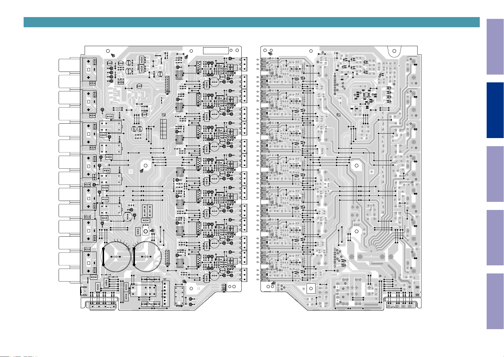
MAIN
1
2
1
2
1
2
1
2
C5211
1
2
C5711
1
2
C5611
1
2
J5802
J5903
BK505
D5819
Before Servicing
This Unit
MAIN (A SIDE) MAIN (B SIDE)
C5803
C5801
C5820
C5819
C5826
J5941
C5810
J5938
R5805
J5801
J5862
C5807
R5803
D5807
J5863
9.AMPSIG_DET
8.THERMAL DET_B
7.DC_PROT
6.DGND
5.ASO_DET
4.MUTE_+B
3.-12V
2.CURRENT_GND
1.CURRENT_DET
R5845
D5816
J5873
ADJ1 ADJ2 RPICTIC
ADJ1 ADJ2 RPICTIC
J5932
J5872
CUP12737Z-1 MAIN PART
J5871
J5870
J5866
J5926
J5925
J5924
J5923
R5827
R5826
C5828
ET502
J5902
J5901
J5900
J5899
T8A L 250V
J5804
1.AC_L
2.NC
3.AC_H
1
4.CEN
5.AC_H
8
6.NC
7.AC_L
T8A L 250V
J5805
C5809
R5825
3
FR
R5824
R5823
R5821
C5113 C5513
3
JK501 JK502JK506 JK507
JK505
3
3
C5411
3
J5884
C5213
3
C5713
3
C5613
~
FL
C5110
R5433
J5880
R5733
J5893
J5892
SBL
J5906
J5907
R5333
J5894
C5812
R5533
5 4
2 3
5 4
2 3
JK504
5 4
2 3
JK503
5 4
2 3
R5633
R5829
J5908
~
C5610
J5895
R5133
C5410
C5120
C5710
SBR
J5909
+
C5510
C5310
SL
J5916
J5915
J5914
J5913
J5912
D5818 D5817
SR
J5910
C5511
C5111
C5313
C5311
C5413
R5233
J5891
C5615
C5813
J5904
J5905
-
J5877
J5876
6
1
J5879
CEN
6
1
6
1
J5886
J5885
6
1
J5898
J5897
J5896
C5811
J5911
D5819
R5806
J5939
R5809
R5842
R5804
C5802
R5841
C5827
J5865
J5935
D5815
J5875
D5802
J5878
J5874
J5937
J5936
RY582
C5825
R5843
R5844
D5804
RY584
J5883
J5882
J5881
D5803
RY583
J5890
J5889
J5888
Q5807
J5887
D5805
RY585
R5819
R5820
C5808
C5816
R5828
J5917
F5801
C5814
J5921
J5922
4
5
J5920
J5919
D5806
C5815
RY586
F5802
J5918
J5934
C5804
C5805
J5858
J5943
R5846
D5809
R5813
R5531
R5532
9
L5501L5401
9
R5530
R5529
R5432
BN501
Pb
R5431
R5430
R5429
D5812
R5816
R5331
R5332
L5301
R5808
R5329
R5330
J5869
J5836
J5835
J5868
J5834
J5867
J5832
L5201
R5232
R5814
R5231
R5807
R5230
D5808
D5810
R5812
R5131
R5132
L5101
R5130
R5129
D5814
R5818
R5731
R5732
L5701
(OPTION)
8.SB_RLY
7.C/S_RLY
6.FRONT_RLY
R5730
5.+12V
4.HI-B_RLY
3.H/P_RLY
2.RLY_GND
R5729
1.THERMAL DET_A
D5813
R5817
8
R5632
L5601
BN502
R5630
J5861
R5629
J5860
RY581
CN502
D5801
J5933
R5527
CN55B
6
J5857
7.AGND
5-6.FR
2
17
3-4.PRE_-B
1-2.FB_FR
J5856
R5524
R5525
J5855
J5854
J5853
J5852
J5851
R5523
R5427
J5850
D5811
R5815
CN54B
62
7.AGND
5-6.SR
17
3-4.PRE_-B
1-2.FB_SR
J5849
R5424
R5425
J5848
J5847
J5846
J5845
J5844
R5327
J5843
CN53B
6 2
7.AGND
5-6.CEN
17
3-4.PRE_-B
1-2.FB_CEN
J5842
R5324
J5841
J5840
J5839
J5838
J5837
R5227
6 2
17
CN52B
J5831
7.AGND
5-6.SL
3-4.PRE_-B
1-2.FB_SL
R5224
J5830
J5829
J5828
J5827
J5826
R5127
J5825
R5229
CN51B
6 2
7.AGND
5-6.FL
2
17
3-4.PRE_-B
1-2.FB_FL
J5824
R5124
R5125 R5225 R5325
J5823
J5822
J5821
J5820
J5819
R5727
J5818
CN57B
6
7.AGND
5-6.SBR
3-4.PRE_-B
17
1-2.FB_SBR
J5817
J5816
BN59B
BN58B
R5725
R5724
J5815
J5814
J5813
J5812
J5811
R5723 R5123 R5223 R5323 R5423
R5631
R5627
J5810
CN56B
6 2
7.AGND
5-6.SBL
3-4.PRE_-B
17
1-2.FB_SBL
J5809
J5808
R5624
J5807
J5806
J5803
R5623
R5802
J5859
R5801
BAR CODE
R5518
CUP12737Z-1 MP 2015.02.27
J5501
R5520
R5522
J5502
CN550
VR550
Q5506
R5514
2SB1560
Q5504
KTC3114
D5504
CN540
D5404
CN530
D5304
CN520
D5204
CN510
D5104
CN570
D5704
CN560
D5604
E C B
BN55A
FR
Q5505
2SD2390
R5513 D5505
R5517
D5502
E C B
R5512
R5515
R5418
C5507
R5516
J5401
VR540
Q5406
2SB1560
R5414
Q5404
E C B
KTC3114
BN54A
BN54B BN55BBN56B
Q5405
2SD2390
D5405
R5413
D5402
R5417
R5412
R5415
C5407
R5318
R5416
J5301
VR530
Q5306Q5305
R5314
2SB1560
E C B
Q5304
KTC3114
BN53A
CEN
BN53B
2SD2390
R5313
D5305
R5317
D5302
E C B E C B
R5315
R5312
R5218
C5307
R5316
J5201
VR520
Q5206
R5214
2SB1560
E C B
Q5204
KTC3114
BN52A
SL SR
Q5205
2SD2390
D5205
R5213
D5202
R5217
E C B
R5212
R5215
R5118
C5207
R5216
B E B EB E B EB E B EB E B EB E B E
B
J5101
VR510
Q5106
R5114
C
2SB1560
E
Q5104
KTC3114
BN51A
FL
BN51B BN52B
Q5105
2SD2390
R5113
D5105
D5102
R5117
E C B
R5112
R5115
R5718
C5107
R5116
B E B E
J5701
VR570
Q5706
R5714
2SB1560
E C B
Q5704
KTC3114
BN57A
SBRSBL
BN57B
Q5705
2SD2390
R5713
D5705
R5717
D5702
R5715
R5712
E C B
R5618
C5707
R5716
B E B E
J5601
VR560
Q5606
R5614
2SB1560
E C B
Q5604
KTC3114
BN56A
Q5605
2SD2390
D5605
R5613
D5602
R5617
E C B
R5612
R5615
C5607
R5616
R5726 R5626R5526 R5426 R5326 R5226 R5126
Q5508
Q5507 Q5307 Q5207 Q5107Q5407
Q5408
Q5308
Q5208
Q5108
Q5708
Q5707
Q5608
Q5607
J5504
R5519
R5521
C5509
C5508
D5503
J5503
R5420
R5422
J5402
J5404
R5419
R5421
C5409
C5408
D5403
J5403
R5320
R5322
J5302
J5304
R5319
R5321
C5309
C5308
D5306 D5406 D5506
D5303
J5303
R5220
R5222
J5202
R5228 R5328 R5428 R5528
J5204
R5219
R5221
C5209
C5208
D5206
D5203
J5203
R5120
R5122
J5102
R5128
J5104
R5119
R5121
C5109
C5108
D5106
D5103
J5103
R5722R5720
J5702
J5704
R5719
R5721
C5709
C5708
D5703
J5703
R5622R5620
J5602
R5628 R5728
J5604
R5619
R5621
R5625
C5608
D5606 D5706
D5603
J5603
C5609
3.HP_LCH
2.AGND
1.HP_RCH
BN503
B_DETECT(OPT.)
Q5810
R5810
Pb
Q5813
C5806
R5811
9.AMPSIG_DET
8.THERMAL DET_B
7.DC_PROT
6.DGND
5.ASO_DET
4.MUTE_+B
3.-12V
2.CURRENT_GND
1.CURRENT_DET
Q5806
Q5801
Q5812
Q5809
R5837
R5835
C5823
R5834
R5830R5831
8.SB_RLY
7.C/S_RLY
6.FRONT_RLY
5.+12V
4.HI-B_RLY
3.H/P_RLY
2.RLY_GND
1.THERMAL DET_A
Q5811
C5512
Q5814
Q5808
R5836
C5818
C5817
IC501
R5832
R5840
R5839
Q5805
C5824
R5838
R5833
Q5802Q5804Q5803
C5821
C5112
C5312
C5412
C5212
C5712
C5612
Electrical Mechanical Repair Information Updating
29
Page 30
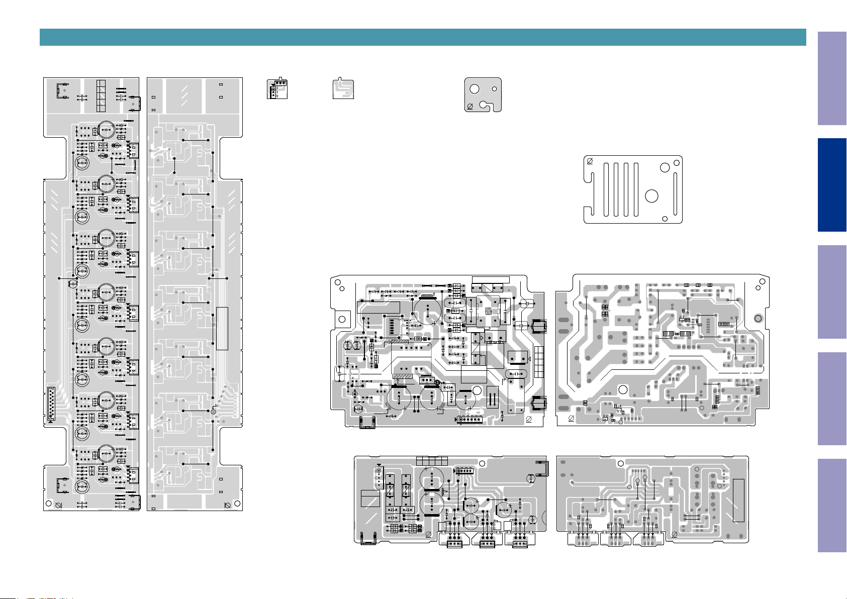
DIFF-AMP, BIAS-TR, PHONE WIRE GUIDE, HDMI CABLE GUIDE, SMPS, REGULATOR
Before Servicing
This Unit
DIFF-AMP (A SIDE) DIFF-AMP (B SIDE) BIAS-TR (A SIDE) PHONE WIRE GUIDE (A SIDE)BIAS-TR (B SIDE)
15.+12V
14.AGND
13.SBL
12.AGND
11.SBR
10.AGND
9.FL
8.AGND
7.SL
6.AGND
5.CEN
4.AGND
3.SR
2.AGND
1.FR
11 115
CN201
MP_STAGE
CUP12618Z
DIFF-AMP PART
J2902
C2901
C2900
BK201
CMD1A569
R2603
J2602
R2604
R2605
R2602
R2601
R2703
J2702
R2704
R2705
R2702
R2701
J2103J2203
R2103
R2104
R2105
R2102
R2101
J2801
R2203
J2202
R2204
R2205
R2202
R2201
J2303
R2303
J2302
R2304
R2305
R2302
R2301
14
J2403 J2703
R2403
J2402
R2404
R2405
2 10
R2402
R2401
J2503
R2503
J2502
R2504
R2505
R2502
R2501
BK203
CMD1A569
C2905
C2904
Pb
J2901
C2903
ADJ1IC ICT RPADJ2
C2902
Q2602
C2605
Q2601
C2603
C2602
C2604
R2607
R2606
C2601
J2705
Q2702
C2705
Q2701
C2703
C2702
R2710
C2704
Q2703
R2707R2711
R2706
J2701
C2701
Q2102
Q2101
C2105
J2102
C2103
C2102
R2110
C2104
Q2103
R2107
R2111
R2106
J2101
C2101
C2800
Q2202
C2205
Q2201
C2203
C2202
R2210
C2204
Q2203
R2207
R2211
R2206
J2201
C2201
Q2302
C2305
Q2301
C2303
C2302
R2310
C2304
Q2303
R2307
R2311
R2306
J2301
C2301
Q2402
C2405
Q2401
C2403
C2402
R2410
C2404
Q2403
R2407
R2411
R2406
J2401
C2401
Q2502
C2505
Q2501
C2503
C2502
R2510
C2504
Q2503
R2507
R2511
R2506
J2501
C2501
J2904
J2903
C2907
C2906
CMD1A387
BK202
CMD1A387
D2601
R2608
R2609
C2606
J2606
R2610
Q2603
7
R2611
J2601
D2701
R2708
R2709
C2706
1
7 1
D2101
R2108
R2109
C2106
7 1
D2201
R2208
R2209
C2206
7 1
D2301
R2308
R2309
C2306
7 1
D2401
R2408
R2409
C2406
7 1
D2501
R2508
R2509
C2506
71
J2504
BK204
CN56A
SBL
CN57A
CN51ACN52A
J2104
CN53A
CN54A
J2404
CN55A
CMD1A387
4
J2605
J2604
4
J2704
4
4
J2204
4
J2304
4
4
1.FB_SBL
2.FB_SBL
3.PRE_AGND
4.PRE_AGND
5.SBL
6.SBL
7.AGND
1.FB_SBR
2.FB_SBR
3.PRE_-B
4.PRE_-B
5.SBR
6.SBR
7.AGND
SBR
1.FB_FL
2.FB_FL
3.PRE_-B
4.PRE_-B
5.FL
6.FL
7.AGND
1.FB_SL
2.FB_SL
3.PRE_-B
4.PRE_-B
5.SL
6.SL
7.AGND
SL FL
1.FB_CEN
2.FB_CEN
3.PRE_-B
4.PRE_-B
5.CEN
6.CEN
7.AGND
CEN
1.FB_SR
2.FB_SR
3.PRE_-B
4.PRE_-B
5.SR
6.SR
7.AGND
1.FB_FR
2.FB_FR
3.PRE_-B
4.PRE_-B
5.FR
6.FR
7.AGND
FR SR
1.FB_SBL
2.FB_SBL
3.PRE_AGND
4.PRE_AGND
5.SBL
6.SBL
7.AGND
2.FB_SBR
3.PRE_-B
4.PRE_-B
5.SBR
6.SBR
7.AGND
1.FB_FL
2.FB_FL
3.PRE_-B
4.PRE_-B
5.FL
6.FL
7.AGND
1.FB_SL
2.FB_SL
3.PRE_-B
4.PRE_-B
5.SL
6.SL
7.AGND
1.FB_CEN
2.FB_CEN
3.PRE_-B
4.PRE_-B
5.CEN
6.CEN
7.AGND
1.FB_SR
2.FB_SR
3.PRE_-B
4.PRE_-B
5.SR
6.SR
7.AGND
1.FB_FR
2.FB_FR
3.PRE_-B
4.PRE_-B
5.FR
6.FR
7.AGND
CMD1A387
1.FB_SBR
J2705
CMD1A569
J2602
J2703
J2702
J2103
J2102
J2203
J2801
J2202
BAR CODE
LABEL
J2303
15.+12V
14.AGND
13.SBL
J2302
12.AGND
11.SBR
10.AGND
9.FL
8.AGND
7.SL
6.AGND
5.CEN
4.AGND
3.SR
2.AGND
1.FR
J2403
CN201_15 PIN
(+12V TP)
J2402
J2503
J2502
CMD1A569
Pb
BE
Q2104
KTC3114
BN51A
B E
KTC3114
CUP12910Z-1
SMPS PART
MP_STAGE
C6023
Sec.
Pri.
C6008 C6013
ZD620
R6017
R6021
C6010
BK603
1A629
BK303
J6004
J6007
R6015
J6009
ZD618
IC602
R6016
J6013
R6018
D6010
1.AC_S2
2.NC
3.RTN_GND
4.NC
5.AC_S2
AC120V
F3003/F3004
AC100V
AC220~230V
F3001/F3002
1A387
ZD621
BAR CODE
R6004
R6010
D6007
Pri.
Sec.
IC603
BONDING
D6008
BONDING
1 5
CUP12737Z-3 MP 2015.02.27
Pb
HDMI CABLE GUIDE (A SIDE)
Pb
SMPS (A SIDE) SMPS (B SIDE)
J6003J6002
ZD609
ZD610
R6009 R6008
J6017
12 7
S
S
S
S
S
S
J6018
T6001
J6012
C6019
ZD619
CUP12910Z-2
REGULATOR PART
MP_STAGE
CN302
T 1.25A L 250V
T 1.25A L 250V
F3003
F3001
C3003
C3005
D3003
D3004
BONDING
ZD608
IC601
BONDING
T 1.25A L 250V
F3002
J6016
V
X
C
F
6
J6005
D6005
C6003
D6004
C6004
D6002
ZD601
D
D6012
D6013
J6020
J6019
REGULATOR (A SIDE) REGULATOR (B SIDE)
T 1.25A L 250V
F3004
C3004
J3004
J3006
D3001
D3002
1 7
14 8
C6018
BONDING
FCT1 FCT2 RPICTMI
C3007
Pb
ZD611
J6010
ZD613
ZD617
ZD614
ZD616
Pri.
Sec.
J6001
R6034
C6027
C6028
1.D5.2V
5.D_GND
4.D_GND
3.M_RESET
2.D5.2V
6.MAIN POWER
BN601
C3006
J3023
BONDING
D3104
C3013
1 .GND
2 .IN
3 .-12V
J3026
J3027
BOTTOM SIDE BOTTOM SIDE BOTTOM SIDE
T1.6A L 250V
T2A L 250V
D6006
D6001
D6003
C6002
3
CX602
LF602
CLZ9Z126Z:E3,K
CLZ9Z133Z:E2,E1C
ZD612
ZD615
F6002
AVR-S530BT/X540BT
T 2.5A L 250V
(AC220V~230V AREA)
T 5A L 250V
(AC100V~120V AREA)
C6017
OPEN
OPEN
6
5.DA+5V
3.+12V
1.-12V
2.RLY_GND
4.VGND
BN301
5
J3025
J3024
C3012
J3035
J3036
J3028
J3030
J3037
KIA7912 KIA7812
IC302
(AC220V~240V AREA)
(AC100V~120V AREA)
CX601
142
LF602
T 6.3A L 250V
T 3.15A L 250V
(AC100V~120V AREA)
(AC220V~230V AREA)
AVR-S730H/X1400H
J6015
J6014
D6009
J3015
D3103
C3008
1 .IN
2 .GND
3 .+12V
J3031
IC301
F6001
J6011
CN602
CN601
C6001
BONDING
4 3
RY601
1 .IN
2 .GND
3 .+5VV
J3032
R6027
R6029
L N
Pri.
C6022
C6021
C3002
R6030
R6028
C6029
R6024
Q6003
IC604
R6025
MAIN_POWER TP
C3009
C3010
CY602
BK601
1A834
CY601
LN
FCT1 FCT2 RPICTMI
Pri.
2
Sec.
BK602
1A834
1
Pb
BK301
1A569-V1
C3024
D3101
D3108
J3013
C3001
J3033
J3034
I OG I G O OG I
IC305
KIA7805BPI
Sec.
Pb
CUP12737Z-4 MP 2015.02.27
L6001
C6030
5.DA+5V
4.VGND
+12V TP
DA+5V TP
C3014
Electrical Mechanical Repair Information Updating
R6033R6032R6031
R6006
R6013
R6014
V
Q6002
X
C
F
C6026
C6011
R6011
D
Pri.
Sec.
C6015
C6014
3.+12V
2.RLY_GND
1.-12V
-12V TP
C3011
AC_S2 TP
C3015
Pb
C6012
D5.2V TP
C6009
C6007
C6006
C6005
S
S
R6012
S
S
S
S
R6022
R6023
C6020
R6020
R6019
AC_S2 TP
Sec.
Pri.
Pri.
Sec.
C6024
C6025
R6026
1.AC_S2
2.NC
3.RTN_GND
4.NC
5.AC_S2
BAR CODE
30
Page 31

FRONT, PHONE, USB WIRE GUIDE, STANDBY, MIC, USB
5
Before Servicing
This Unit
PHONE (A SIDE) PHONE (B SIDE)
CN104
LUG13
C1067 C1065
3287
BN131
STANDBY (A SIDE)
J1111
J1113
SW101
J1112
D1012
J1114
BN101
1
JK104
D1002
C1429
R W
9
MIC (A SIDE)
JK105
5
1
3
4
2
6
7
LUG14
C1083
L1012
C1069
R1057
1.D GND
3.H/P DET
2.D GND
J1106
D1401
C1402
J1110
1.H/P R
L1010
3.H/P L
2.A GND
C1072 C1071
C1084
C1424
L1011
C1068
L1013
C1066
VR102
BN12B
C1405
J1108
J1107
C1407
C1411
USB (A SIDE)
JK101
C1052
J1105
1 432
FRONT (A SIDE) FRONT (B SIDE)
LUG11
BAR CODE
CUP12957Z-1/FRONT PART/MP STAGE
GNDGND
VR101
C1076
C1077
1.A GND
2.MIC SIGNAL
3.-12V
4.+12V
-12V
S540BT : ADJUST
S640H/S740H : PURE
R1071
S540BT : ADJUST
S640H/S740H : GAME
R1082
R1081
R1086
R1076
Q1024
Q1021
Q1020
Q1019
R1090
/S740H : Q/S_4
R1079
S540BT/S640H
S540BT/S640H/S740H : Q/S_3
R1085
S540BT/S640H/S740H : Q/S_2
GNDGND
S540BT/S640H/S740H : Q/S_1
R1075
1.D GND
8.MCU+5
7.RED_LED
9.POWER_KEY
C1081
5.MIC DET
C1409
R1410
+12V
S540BT/S640H/S740H : ADJUST
X250BT/X550BT/X1500H : Q/S_4
R1078
R1084
R1087
R1083
R1072
R1077
R1073
GNDGND
Pb
R1074
GNDGND
3.ISEL_B
2.ISEL_A
5.DGND
4.DGND
1.+3v3
6.GRN_LED
C1091
C1090
C1089
C1088
C1082
R1046
X250BT/X550BT/X1500H : Q/S_3
S540BT/S640H/S740H : DIMMER
Cushion
X250BT/X550BT/X1500H : Q/S_2
S540BT/S640H : SLEEP
S740H : MODE
S540BT : MODE
S640H : INFO
S740H : BAND
X250BT/X550BT/X1500H : Q/S_1
S540BT/S740H : TUNE+
X250BT/X550BT/X1500H : STATUS
S640H : MODE
X250BT/X550BT/X1500H : DIMMER
S540BT/S740H : TUNE-
S640H : BAND
X250BT/X550BT/S640H : TUNE+
S540BT/S740H : PRESET+
X1500H : ZONE2 SEL
S540BT/S740H : PRESET-
X250BT/X550BT/S640H : TUNE-
X1500H : ZONE2 ON/OFF
R1022
S640H/X1500H : PRESET+
X250BT/X550BT : PRESET+
S740H : ZONE2 SEL
S540BT : SOUND
R1024
C1039
S640H/X1500H : PRESET-
S740H : ZONE2 ON/OFF
X250BT/X550BT : PRESET-
S540BT : SOUND
R1008
R1005
+3.3V
C1087
C1086
C1085
GND
R1023
D1402
D1403
J1102
C1075
J1095
J1099
J1098
J1097
J1096
J1094
BN12B1
USB WIRE GUIDE (A SIDE)
J1093
J1092
1 21
11
J1090
220 10
J1088
J1089
J1084
Pb
J1053
C1017
J1051
5
8
Q1001
J1047
J1046
J1045
43
50
53
J1005
57
J1004
C1007
Q1014
R1424
F1001
STANDBY (B SIDE)
D1407
R1411
R1412
+12V
-12V
5.MIC DET
4.+12V
3.-12V
2.MIC SIGNAL
1.AGND
+5V
L1003
L1404
C1051
L1004
C1053
D1008
D1020
D1019
D1406
C1428
A
C1426
C B
R1416
C1425
+12V
1.+3v3
6.GRN_LED
7.RED_LED
8.MCU+5
9.POWER_KEY
5.DGND
2.ISEL_A
3.ISEL_B
4.DGND
MIC (B SIDE)
R1408
C1408
R1409
IC101
5 8
C1417
C1413
R1407
C1414
R1433
R1435
R1027
C1406
4
C1415
C1416
R1434
R1431
R1436
C1450
R1432
R1437
C1451
1.VBUS
3.USBD-
4.DGND
5.DGND
2.USBD+
R1040
D1011
C1050
L1005
C1049C1048
D1010D1009
Pb
R1042
R1041
R1045
C1055
Q1009
C1427
R1414
R1415
R1413
L1402
L1401
R1401
R1054
C1401
R1402
R1403
R1405
R1404
R1406
C1404
C1403
D1404
D1405
Pb
Q1008
Q1012
C1054
R1043
R1044
Q1011
+5V
Pb
L1403
C1452
J1104
C1410
USB (B SIDE)
5
BN104
27
C1010
J1052
BK101
J1050
J1049
FL101
J1048
J1033
R1067
R1030
R1423
BK102
R1427
C1004
R1426
R1425
R1062
R1007
C1006
D1001
1 7
J1083
J1082
26
C1019
J1054
J1055
J1056
J1115
J1075
J1057
J1058
J1060
J1044
J1043
J1041
J1042 J1059
J1040
J1039
J1038
J1037
J1036
J1034
J1035
J1032
J1007
J1006
J1015
J1008
J1009
C1038
J1010
LD101
J1064
RC101
D1003
D1005
C1005
C1003
C1002
J1001
R1002
R1001
CN102
C1001
BN12A
J1101
J1100
5
J1091
SW111
J1087
J1086
J1085
J1078
J1081
J1079
J1077
J1076
SW110
J1067
J1061
J1028
J1062
J1063
J1031
SW116
J1029
J1109
SW109
J1002
R1004
R1003
SW102
J1074
J1080
J1073
J1072
SW118
J1071
J1070
J1068
SW103
SW114
S640H/S740H : MUSIC
S540BT : BASS/TREBLE
S640H/S740H : MOVIE
S540BT : ON/OFF
J1066
J1065
SW108
SW117
BN10
J1027
J1026
J1025
SW104
J1020
J1022
J1021
J1019
J1018
J1103
R1092
Q1023
Q1022
Q1017
J1023
J1024
R1091
Q1018
J1017
J1014
J1016
J1069
SW119
J1013
SW105
R1080
SW113 SW112
J1030
J1012
SW115
SW107
J1011
J1003
9
SW106
BN101_1
1 3
CN103
3.H/P DET
2.D GND
R1068
R1011
R1010
Q1002
R1053
R1418
Q1016
R1421
R1420
R1419
R1009
R1006
R1020
R1021
R1069
C1009
C1073
C1074
D1015
D1016
GNDGND
R1017
R1019
Q1007
R1430
Q1006
R1015
R1014
R1013
Q1005
R1026
R1058
R1061
R1060
R1059
-12V
R1012
R1429
1.ISEL_A
2.ISEL_B
3.MIC_DET
4.POWER_KEY
5. +12V
6. -12V
7.MIC_SIGNAL
8.A_GND
9.B/P_IRIN_DE
10.H/P_DET
11.VSEL_A
12.VSEL_B
13.KEY_3
14.KEY_2
15.KEY_1
16.RED_LED
17.GRN_LED
18.RC_IN
19.FL_RST
20.FL_CE
21.FL_CLK
22.FL_DATA
23.CPU_POWER
24.MCU_5V
25.MCU_3V3
26.D_GND
27.NET_FACT_RST
Pb
+12V
+3V3
Electrical Mechanical Repair Information Updating
L1001
R1422
C1011
C1041
C1020
Q1004
R1018
R1016
Q1003
R1025
GNDGND
C1013
C1014
C1015
C1016
C1012
C1423
D1408
C1430
Q1013
R1428
Q1015
2.NC
3.GND
4.NC
5.FL AC
6.NC
7.FL AC
1.VDISP
31
Page 32

LEVEL DIAGRAM
FRONT ch
Before Servicing
This Unit
AVRS740H/X1500H LEVEL DIA G RAM
NJ U72340A
LIN E IN
MIC IN
+20dB
+10dB
LIN E IN 0dB
(200m V)
-10dB
-20dB
MIC IN
11.48m Vrm s
-30dB
-40dB
AD C
851mV rms
-8. 5dB
AD IN=319m Vrm s
-8. 5dB
AD IN=75m Vrm s
+37. 60dB
ACM 2(D M-A 409)Sensit ivity :
-38.8dBV/ Pa=11. 48mV/ Pa a t 94dBSPL@ Oper ation V oltage 5.0V
(94dBSPL is ex pected to -11.0dB FS)
PCM 9211
AD C
PCM 9211
SING LE INPU T
0dBFS =3V pp=1.06V rms
0dBFS
-10dBF S
-20dBF S
-26.5dB FS
-30dBF S
-40dBFS
PL D
5M 570ZF256C5N
DS P
CS49844A
SW : YES
-20dBFS( DIG. IN)
-23dBF S(A/ D IN)
SW : NON E
-32dBFS( DIG. IN)
-35dBFS( A/D IN)
1.98V rms =0dBF S
-10dBF S
-20dBF S
-30dBF S
-40dBFS
DA C
AK4458V N
DA C
AK4458
L.P .F G AIN = + 0.4dB
FRONT CHA NNEL
FULL SCAL E LE VEL =2.0 Vrm s
DO LBY LIMIT LEVEL= 1. 41Vrm s (A LL ch -3dB FS)
GA IN se tting of M ASTER VO L 00dB
- S W:Y ES (DIG ITAL)
- S W:YES (ANA LOG)
- S W:N ONE (DIG ITA L)
- S W:N ONE (AN ALOG)
(1) :Bas ic O FFSET of VOL =0dB (Indicat ion valude)
(2) :Fine-t uning by softw are Digita l input
(3) :Volt age due to hardw are of analog input
(4) :OFFSE T of SW NON
NJ U72343V
GA IN
ADJ .
VO LUM E IC : N JU72343 NON CLIP MAX SIGN AL LEVE L 4. 2Vrm s
-2. 5dB
-2. 5dB
LIN E IN
+0 .5dB
+9 .5dB
+12. 5dB
-0. 5dB
-2. 0dB
-2. 0dB
-2. 0dB
-2. 0dB
-0. 5dB
-0. 5dB
-0. 5dB
(1)
(2) (3 )
+12dB
+12dB
(4) (5)
+3. 0dB
+3. 0dB
=-2 .5dB
=+1dB
=+9.5dB
=+13dB
PO WE RAM P G AIN
+29dB
ANA LOG
H/P OU T
SPK O UT
FR ONT
H/P OU T
+30dB
SPK O UT
4.27V rms /8ohm
+20dB
+10dB
H/P OU T
277mV rms /33ohm
0dB
(200m Vrm s)
PR EOU T 150m Vrm s
-10dB
-20dB
-30dB
-40dB
Electrical Mechanical Repair Information Updating
-50dB
-50dB
32
Page 33

CENTER, SURROUND ch
Before Servicing
This Unit
AVRS740H/X1500H LEVEL DIA G RAM
PL D
5M 570ZF256C5N
DS P
CS49844A
+20dB
+10dB
2CH IN 0dB
(200m V)
-10dB
-20dB
-30dB
1.98V rms =0dBF S
SW :YES
-20dBF S(D IG.IN )
-23dBF S(A /D IN )
-10dBF S
-30dBF S
-40dBFS
DA C
AK4458V N
-20dBF S
CENT ER/SURRO UND CHANNEL
NJ U72343V
VO LUM E IC : N JU72343 NON CLIP MA X SI GNA L LE VEL 4. 2Vrm s
DA C
AK4458
L.P .F G AIN = + 0.4dB
FULL SCAL E LE VEL =2.0 Vrm s
DO LBY LIMIT LEVEL= 1. 41Vrm s (A LL ch -3dB FS)
GA IN se tting of M ASTER VO L 00dB
- S W:Y ES (DIG ITAL)
- S W:Y ES (DIG ITAL)
(1) :Basic OFFSET of VO L= 0dB (Indic ation v alude)
(2) :Fine-t uning by softw are Digita l input
(3) :Volt age due to hardw are of analog input
(4) :OFFSE T of SW NON
-2. 5dB
+0 .5dB
-2. 0dB
-2. 0dB
(1)
-2. 5dB
LIN E IN
-0. 5dB
-0. 5dB
(2)
Electrical Mechanical Repair Information Updating
SPK O UT
CE NTER
GA IN
ADJ .
+30dB
SPK O UT
4.27V rms /8ohm
PO WE RAM P G AIN
+29dB
=-2 .5dB
=+0.5dB
+3. 0dB
(3)
(4)
+20dB
+10dB
0dB
(200m Vrm s)
PR E O UT
150mV rms
-10dB
-20dB
-30dB
-40dB
-50dB
-40dB
-50dB
33
Page 34

SURROUND BACK ch
Before Servicing
This Unit
AVRS740H/X1500H LEVEL DIA G RAM
PL D
+20dB
+10dB
2CH IN 0dB
(200m V)
-10dB
-20dB
-30dB
5M 570ZF256C5N
DS P
CS49844A
AK4458V N
1.98V rms =0dBF S
-10dBF S
-20dBF S
SW :YES
-20dBFS( DIG .IN)
-23dBF S(A /D IN )
-30dBF S
-40dBFS
DA C
SURRO UND BACK CHANNEL
DA C
AK4458
L.P .F G AIN = + 0.4dB
FULL SCAL E LE VEL =2.0 Vrm s
DO LBY LIM IT L EVEL= 1.41Vr ms (ALL c h -3dB FS)
GA IN se tting of M ASTER VO L 00dB
- S W:Y ES (DIG ITAL)
- S W:Y ES (DIG ITAL)
(1) :Basic OFFSET of VO L= 0dB (Indic ation v alude)
(2) :Fine-t uning by softw are Digita l input
(3) :Volt age due to hardw are of analog input
(4) :OFFSE T of SW NON
NJ U72343V
VO LUM E IC : N JU72343 NON CLIP MAX SIGN AL LEVE L 4. 2Vrm s
-2. 5dB
LIN E IN
-2. 5dB
+0 .5dB
-2. 0dB
-2. 0dB
(1)
-0. 5dB
-0. 5dB
(2)
=-2 .5dB
=+0.5dB
+3. 0dB
(3)
(4)
Electrical Mechanical Repair Information Updating
SPK O UT
SURRO UND BA CK
GA IN
ADJ .
+30dB
SPK O UT
4.27V rms /8ohm
PO WE RAM P G AIN
+29dB
+20dB
+10dB
(200m Vrm s)
0dB
PR E O UT
150mV rms
-10dB
-20dB
-30dB
-40dB
-50dB
-40dB
-50dB
34
Page 35

SUBWOOFER ch
Before Servicing
This Unit
AVRS740H/X1500H LEVEL DIA G RAM
PL D
5M 80ZT
DS P
CS49844A
+20dB
+10dB
2CH IN 0dB
(200m V)
-10dB
-20dB
-30dB
-40dB
PCM INP UT:- 20dBFS L+R
ANA INPU T:200m Vrm s L +R 30H z
DD INP UT:- 30dBFS LFE 30Hz
1.98V rms =0dBF S
-34dBFS( DIG. IN:PC M)
-37dBF S(A/ D IN)
-40dBFS
(DIG .IN: DD)
-10dBF S
-20dBF S
-30dBF S
-40dBFS
-50dBFS
SUBW OOFER CHA NNEL
DA C
PCM 1690
DA C
AK4458
L.P .F G AIN = + 6.5dB
FULL SCAL E LEVE L
DO LBY LIMIT LEVEL= 1. 41Vrm s (A LL ch -3dB FS)
NJ U72340A
VO LUM E IC : N JU72343 NON CLIP MAX SIGN AL LEVE L 4. 2Vrm s
-2. 5dB
LIN E IN
+11. 5dB
+11. 5dB
GA IN se tting of M ASTER VO L 00dB
- D IGITA L IN
- A NALOG IN
(1) :Basic OFFSET of VO L= 0dB (Indic ation v alude)
(2) :Fine-t uning by softw are Digita l input
(3) :Volt age due to hardw are of analog input
(4) :Corre ction o f Subw oofer
(5) :OFFSE T of A/D input
-2. 0dB
-2. 0dB
-0. 5dB
+14dB
-0. 5dB
(1)
+14dB
(2)
(3)
(4)
+14. 5dB
+3. 0dB
(5)
=+11.5dB
=+14.5dB
Electrical Mechanical Repair Information Updating
MU TE
GA IN
ADJ .
PR E O UT
SU BWOOF ER
+30dB
+20dB
+10dB
PR E O UT
300Vrm s
0dB
(200m Vrm s)
PR E O UT
150Vrm s
-10dB
-20dB
-30dB
-40dB
-50dB
-50dB
35
Page 36

ZONE2 ch
Before Servicing
This Unit
AVRS740H/X1500H LEVEL DIA G RAM
NJ U72340A
LIN E IN
MIC IN
+20dB
+10dB
LIN E IN 0dB
(200m V)
-10dB
BD3812F
NJM 8080 M AX.OU TPUT 7.78V rms
-18dB
+15dB
ZO NE2
NJ U72343V
GA IN
ADJ .
VO LUM E IC : N JU72343 NON CLIP MA X SI GNA L LE VEL 4. 2Vrm s
PO WE RAM P G AIN
+29dB
ANA LOG
SPK O UT
FR ONT
H/P OU T
ZO NE2 OU T
+30dB
SPK O UT
4.27V rms /8ohm
+20dB
+10dB
H/P OU T
277mV rms /33ohm
0dB
(200m Vrm s)
PR EOU T 150m Vrm s
-10dB
Electrical Mechanical Repair Information Updating
-20dB
-30dB
-40dB
-50dB
-20dB
-30dB
-40dB
-50dB
36
Page 37

BLOCK DIAGRAM
ANALOG AUDIO DIAGRAM
Before Servicing
This Unit
AVRS740H /X1500H ANALOG AUD IO BLOCK
VCC:D A+ 5V
TU NER
FM/A M
32.768kHz
AU DIO I N
PH ONO
CB L/SAT
MED IA P LAYE R
AU DYSSE Y
MIC (AUT O SE TUP)
ZON E2
AV RX1500H E3 ON LY
MUT E
VO L IC
BD 3812F
V+ :+7 .5V
* L OGIC CONT ROL HIGH LEV EL INP UT V OLT AGE(M IN: + 2.5V / MAX : V+)
V-: -7.5V
SEL ECT IC
NJU72750V
InA /B1
InA /B2
InA /B3
In
InA /B5
InA /B6
InA /B7
A/ B4
OU TA1
OU TA2
OU TA3
OU TB1
OU TB2
7in 3 out M a tri x-S w it ch
OU TB3
V+ :+7 .5V
* L OGIC CONT ROL HIGH LEV EL INP UT V OLT AGE( MIN: + 2.5V / MAX : V+)
V-: -7.5V
VOLUME IC
NJU72343V
ANA _FL
DA0 1
DA0 2
DA0 3
DA0 4
DA0 5
DA0 6
DA0 7
DA0 8
DA_ FL
ANA _FR
DA_ FR
DA_ CEN
DA_ SW
DA_ SL
DA_ SR
DA_ SBL
DA_ SBR
P-AMP
H/ P OU T
H/ P L
GND
H/ P R
SP K O UT
+
FL
-
+
FR
-
+
CEN
-
+
SL
-
+
SR
-
+
SBL
-
(FL -H/F L-B/B I-AMP-FL/Z ONE- FL)
+
SBR
-
(FR -H/FR -B/B I-AMP-FR /ZON E-FR)
Electrical Mechanical Repair Information Updating
TO DIG ITA L
AU DIO B LOC K
Z2_AD C_L
Z2_AD C_R
NET WOR K
DA_ FL
DA_ FR
DA_ CEN
DA_ SW
DA_ SL
DA_ SR
DA_ SBL
DA_ SBR
AD _FL
AD _FR
ATT.
ATT.
DA0 2
DA0 2
DA0 3
DA0 4
DA0 5
DA0 6
DA0 7
DA0 8
ATT.
ATT.
PR E OU T
MUT E
SW 1
SW 2
37
Page 38

DIGITAL AUDIO DIAGRAM
Before Servicing
This Unit
OP T1(T V)
OP T2(C BL/SAT )
CO AX1( CBL/SA T)
RJ-45 with Tran sform er
F-H DMI IN6
HD MI IN 1
(CB L/SAT )
HD MI IN 2
(D VD)
HD MI IN 3
(B LU-RA Y)
HD MI IN 4
(GAME )
HD MI IN 5
(ME DIA Play er)
E3 ONLY
USB
ET HERN ET
(AU X)
ANT 2
ANT 1
AVRS740H /X1500H D IGITAL AU D IO B LOC K
HD MISPD IF
SPD IF_O UT
OPE N
PC M 9211PT R
NE TW ORK ED ME DIA
IN2
TMD S
IN3
TMD S
IN1
TMD S
IN0
TMD S
Z2_AD C_L
Z2_AD C_R
ADC+ D IR
VCC:D A3.3 V
VCCAD :DA +5V
5V0 :LEGO 5V
LE GO
MOD U LE
(W i th in B T )
IPO D AU TH.
23671011050AS
(MF I337S3959)
P2_RX
P3_RX
P1_RX
P0_RX
H D MI TX(M N864788)
VDD11: C EC1V 1
VDD33:C EC3V 3
AVDD11: CEC1 V1
AVDD33: CEC3 V3
AVDDH 33:CEC 3V3
PVDD33:C EC3 V3
DIR MCK
DIR BCK
DIR LRCK
DIR DAT A
MPIO _B3
MPIO _B2
MPIO _B1
MPIO _B0
DIR XMCK
DIR SLRC K
DIR SBCK
DIR PPCM
DIR 1PERR
DIR AUXM CLK
DIR AUXB CK
DIR AUXL RCK
DIR AUXD ATA
HD MISPD IF
SPD IF_O UT
MCL K_I2 S_0
SCL K_I2 S_0
RXI2 S0/ DSD 1
RXI2 S1/ DSD 2
RXI2 S2/ DSD 3
RXI2 S3/ DSD 4/SP DIF
RXL RCK/ DSD 5
RXB CK/ DSD SCK
RXM CK/ DSD MCK
TX BCK
TX LRCK
TX I2S0
LRC K_I2 S_0
SDO UT_ I2S_ 0
SCL K_I2 S_1
LRC K_I2 S_1
SDO UT_ I2S_ 1
SDO UT_ I2S_ 2
DSP 1INB CK
DSP 1INM CK
SDI N_I2S _0
SDI N_I2S _1
SCL K_I2 S_2
LRC K_I2 S_2
SDI N_I2S _2
TMD S
OUT 0
P0T X
OUT 1
TMD S
P1T X
5M570ZF256C 5N
VCC:D A3.3 V
VCCINT :PLD 1.8V
DSP 1INL RCK
DSP 1INF_ FL
DSP 1INS WC_ C
DSP 1INS _SR
DSP 1INS _SL
AUD IO P LD
DSP 1INR SV_S W
DSP 1INR SV_FR
MVO L_MU TE
VOL UME_ MUTE
APLD _CL K
APLD _D ATA
APLD _CS
PLD ERR
DSP 1OU TS
DSP 1OU TSB
DSP 1OU TF
DSP 1OU TCSW 1
DSP 1OU TFH
DSP 1OU TBC K
DSP 1OU TFS
DSP 1OU TFW
DA CMCK
DA CBCK
DA CLRC K
DA CPCM F
DA CPCM CSW 1
DA CDAT AS
DA CPCM SB
Z2D ACM CK
Z2D ACB CK
Z2D ACL CK
Z2D ACD ATA
PLD ADC DAT A
PLD ADC LRCK
PLD ADC BCK
PLD ADC MCK
(Fro m MC U)
DAC _MUT E
DAC _RST
DAC _MS
DAC _DA TA
DAC _CLK
(Fro m / To M CU)
D AC
AK4458V N
TVDD: DA3 .3V
VRE F:DA +5V
NE T W ORK
D AC(Z2 )
PC M 5100A
ADC(MAIN)
AK5358
VD: DA+ 5V
VA: DA+ 5V
DVDD: 3.3V
CPV DD:3.3V
AVDD: 3.3V
DI GTA L IN
DIR_ CE
DIR_ CLK
DIR_ DIN
DIR_ DOU T
DIR_ RST
(Fro m/T o MC U)
OPT .1
OPT .2
COA X.1
USB D-
USB D+
RX +/-
TX +/-
VDD11: C EC1V 1
VDD33:C EC3V 3
AVDD11: CEC1 V1
AVDD33: CEC3 V3
AVDDH 33:CEC 3V3
PVDD33:C EC3 V3
IN3
AD 8195
TMD S
Bu ffer
TMD S
TMD S
TMD S
TMD S
TMD S
IN2
IN1
IN0
OUT 0
RXD
AD V 7623
H D MI RX( MN864787)
CVDD, DVDD:+ 1V8 H
PVDD:+ 1V8 H
TXA VDD:+ 1V8H
TXP VDD:+ 1V8H
TXP LVDD:+ 1V8 H
DVDDI O:DV 3V3
TVDD: DV3 V3
Z2_AD C_L
Z2_AD C_R
DA _FL
DA _FR
DA _CEN
DA _SW
DA _SL
DA _SR
DA _SBL
DA _SBR
Z2_NE T_L
Z2_NE T_R
AD _FL
AD _FR
Electrical Mechanical Repair Information Updating
ANA LO G AUD IO B LOCK
HD MI O UT
VDD:D A1.0 V
24.576MH z
VDDIO: DA3 .3V
CS49844A
SD RAM
64M/200M Hz
M12L64164A -5TG 2Y
38
D SP
SER IAL FL ASH
64M
EN25Q H64A104H IP
DSP _MOS I
DSP _MISO
DSP _CLK
DSP _RST
DSP _CS
DSP _FLA G0
(Fro m / To M CU)
Page 39

VIDEO DIAGRAM
AVRS740H /X1500H VID EO BLOCK
CVDD, DVDD:+ 1V8 H
PVDD:+ 1V8 H
TXA VDD:+ 1V8H
TXP VDD:+ 1V8H
TXP LVDD:+ 1V8 H
DVDDI O:DV 3V3
TVDD: DV3 V3
Before Servicing
This Unit
F-H DMI IN6
(AU X)
HD MI IN 1
(CB L/SAT )
HD MI IN 2
(D VD)
HD MI IN 3
(B lu-ra y)
HD MI IN 4
(GAME )
HD MI IN 5
(ME DIA PLAY ER)
LEG O
5V0 :LEGO 5V
P3 RX
P2 RX
P1 RX
P0 RX
P1 RX
P0 RX
AVCC: CEC3 .3V
AMUXV CC:CEC 5V
AD 8195
Bu ffer
LEG O_RG B DA TA( 24bit)
HDMI RX(MN864787)
VDD11: C EC1V 1
VDD33:C EC3V 3
AVDD11: CEC1 V1
AVDD33: CEC3 V3
AVDDH 33:CEC 3V3
PVDD33:C EC3 V3
27.000MH z
TXP OR T0
28.6363MHz
P3 RX
P2 RX
P1 RX
P0 RX
RX A
AD V 7623
TRANSCEIVE R
OS D Bl oc k
OT HER : 32M
E2 : 64M
VCC:C EC3V 3
S.F LASH
32M/ 64M
HDMI TX(MN864788)
MAIN
SUB
S.F LASH
32M
VCC:C EC3V 3
P0 T X
P1 T X
27.000MH z
VDD11: C EC1V 1
VDD33:C EC3V 3
AVDD11: CEC1 V1
AVDD33: CEC3 V3
AVDDH 33:CEC 3V3
PVDD33:C EC3 V3
IC751
CP U
CE C
Electrical Mechanical Repair Information Updating
HD MI O UT
MO NITO R O UT
CV BS IN
MED IA P LAYE R
CB L/SAT
NJ M 2595
VCC:+ 5V
VSS:-5 V
75ohm
6dB
20K
20K
20K
20K
Driver
75ohm
6dB
Driver
75ohm
6dB
Driver
CV BS O UT
MO NITO R O UT
39
Page 40

POWER DIAGRAM
!
AC C OR D
REL AY
!
!
S1 (AMP+ B,-B )
S2 (+12V ,-12V)
MAIN T RAN S
S3 (FL+ Vdi sp)
AVRS740H /X1500H VCC D IAGRAM
HI +B
LO W+B
2
4
1
HI -B
3
LO W-B
KIA 7812BPI
KIA 7805BPI
KIA 7912PI
MM1Z7 V5
MM1Z7 V5
MM1Z6 V8
MM1Z6 V8
MM1Z5 V1
MM1Z5 V1
BU33T D3W G
57mA
267.63m A
45mA
122mA
50mA
34mA
AVR X1500H E3 ON LY
22mA
68mA
MAIN+ B
MAIN-B
SEL ETOR IC,V OLUM E IC
(NJ U72750AV, NJU72343V)
A+ 12V
(NJ M8080,SPK /H- P/HI- LOW RELA Y)
DA +3.3 V
(PC M5100A)
DA +5V
(PC M9211PT R,AK4458V N)
(NJ M2740V x 2,AK 5358BET)
TU NER+ 5V
A-12V
SEL ETOR IC,V OLUM E IC
(NJ U72750AV, NJU72343V)
ZON E VO LUME IC
(BD 3812F)
ZON E VO LUME IC
(BD 3812F)
V+ 5V
(NJ M2595)
V-5 V
(NJ M2595)
Vdi sp(+ 37V)
Before Servicing
This Unit
Electrical Mechanical Repair Information Updating
S2 TO TAL : 596. 63mA
!
S4 (FIL AMENT )
INP UT C URRENT (Re f Vo lage :5.2 V)
SM PS Tot al C urren t : A bou t 4901.36m A
D
G
S
12
3 4
*D C-DC Effie cienc y:85%
+5 .2V
MAIN P WR O N
1485.29m A
(5. 2V)
406.83m A
(5. 2V)
332.5m A
(5. 2V)
729.81m A
(5. 2V)
260.526m A
(5. 2V)
TP S563200(+ 3.3V )
TP S563200(+ 1.8V )
TP S563200(+ 1.0V )
TP S563200(+ 1.1V )
NJM2845D L133
2035.18m A
1022.0m A
260.5m A
0.003m A
30mA
20.4m A
1000mA
482.02m A
160.16m A
1054mA
339mA
636mA
982mA
1503.5m A
3000mA
260.5m A
(SN 74CBT 3251PWR)
SW M5V
MCU +5V
CEC 5V
(AD 8195)
D5 V/VB US
DV 5V/H DMI
DA 3.3V /DIR, DSP
(CS 49844A,M12L 64164A-5T G2Y, 5M570ZF 256C5N,T C74VH CU04,M X25L6406E M2I-12G ,PCM9211, AK4458VN )
NET 3.3V /NET WOR K
(IPO D A UTH ,SN74LV C244APW Rx4 )
CEC 3V3 /HD MI
(AD 8195,MN864787, MN864788,M X25L3206E)
DV 3V3
(AD V7623,MX 25L3206E/ MX25L6406E M2I-12G )
LEG O5V
(LEGO )
D1 V8H /HD MI
(AD V7623)
40mA
PLD 1.8V /PLD
(5M 570ZF256C5 N)
DA 1.0V /DSP
(CS 49844A)
CEC 1V1
(MN 864787,MN864788)
SW M3.3 V/LEVE L_CH G
MCU _3V3/ MICO M
(R5 F5631FDDFB, VFD, MC74HC 4094x2)
FRO NT L ED
(CV DBL BJEG J204L)
* T OTA L (5V ): 1050.403m A
163mA
FILAME NT A C
FILAME NT A C
40
Page 41

WIRING DIAGRAM
SM PS PCB
Before Servicing
AVRS740H /X1500H W IRING DIA GRA M
AC C OR D
ANT 1 ANT 2
PCB TO PCB
TUN ER
9P
BN826- 1
CN821
15P
15P
CN825
9P
BN826- 2
SM PS< -AC I N
CN602
2P
CN601
2P
TR ANS - > S MPS
5P
BN301
REG UL.-> DIG ITAL
SM PS-> DIG ITAL
CN823
5P
CN741
6P
D IGIT AL PCB
CN762
8P
CN701
23P
CN321
5P
LE GO
42P
CN502
64P
CN501
CN751
27P
15P
PCB TO PCB
CN822
CN761
9P
RE G. PCB
5P
6P
BN601
CN302
8P
BN502
CN502
7P
CN 201
15P
TRA NS -> REG UL.
PCB TO PCB
MAIN PCB
9P
BN501
This Unit
Electrical Mechanical Repair Information Updating
TRANS
TR ANS - > FR ONT
FU NC TI ON
EN CO D ER
BN101
PO W ER
LE D PCB
BN503
3P
BN56B
3P
7P
CN56A
PCB TO PCB
CN56B
BN57B BN51B
3P
7P
CN57A CN51A CN52A
PCB TO PCB
CN57B CN51B
3P
7P
PCB TO PCB
FRO NT< ->D IGITA L
BN52B
3P
D IFF-AMP PCB
7P 7P
PCB TO PCB
CN52B CN53B
CN53A
PCB TO PCB PCB TO PCB PCB TO PCB
BN53B
3P
BN54B BN55B
3P
7P
CN54A CN 55A
CN55B
CN54B
3P
7P
TR ANS-> MAIN
BN51A
3P
CN102
7P
BN51A BN 51A
3P
3P
FRONT PCB
BN101_1
9P
9P
CN103
3P
H/ P-FRO NT
BN131
H /P PCB
H/ P <- MAIN
3P
3P
CN104
MIC PCB
BN12A
5P
5P
BN12B
MIC
H DM I PCB
HD MI -> DIG ITAL
23P
CN811
BN51A
3P
27P
BN12B 1
BN51A
3P
BN51A
3P
BN51A
3P
US B -> DIG ITAL
5P
BN104
US B PCB
41
Page 42

SEMICONDUCTORS
Only major semiconductors are shown, general semiconductors etc. are omitted to list.
The semiconductor which described a detailed drawing in a schematic diagram are omitted to list.
1. IC's
R5F5631FDDFB(DIGITAL_MCU : IC751)
109
PE2
110
PE1
111
PE0
112
P64
113
P63
114
P62
115
P61
116
VSS
117
P60
118
VCC
119
PD7
120
PD6
121
PD5
122
PD4
VREFL0
VREFH0
123
PD3
124
PD2
125
PD1
126
PD0
127
P93
128
P92
129
P91
130
VSS
131
P90
132
VCC
133
P47
134
P46
135
P45
136
P44
137
P43
138
P42
139
P41
140
141
P40
142
AVCC0
143
P07
144
RX63N Group
RX631 Group
PLQP0144KA-A
(144-pi n LQFP)
(Top view)
R5F56108VNFP Terminal Functions
Pin Pin Name Symbol I/O Pu/Pd STBY STOP
1 AVSS0 AVSS - - - - Ground pin
2 P05/IRQ13 POWER_KEY I M3VPu I I I
3 VREFH VREFH - - - - Reference power supply pin
4 P03/IRQ11 RED_LED O L/H L H POWER/STANDBY LED control pin
5 VREFL VREL - - - - Ground pin
P02/SCK6/IRQ10/
6
AN020
P01/RXD6/IRQ9/
7
AN019
P00/TXD6/IRQ8/
8
AN018
9 PF5/IRQ4
10 EMLE EMLE I Pd - - -
11 PJ5 VSEL_A I SW3VPu I I I Master volume (Rotary encoder) signal input pin
12 VSS VSS - - - - Ground pin
13 PJ3 VSEL_B I SW3VPu I I I Master volume (Rotary encoder) signal input pin
14 VCL VCL I - - - Smoothing capacitor connection pin
15 VBATT VBATT - - - - Power supply pin
16 MD/FINED MD I M3VPu I I I
17 XCIN XCIN I Pd - - - NC(Pull down)
18 XCOUT XCOUT I - - - NC(open)
19 RES# RESET I - - - Reset signal input pin
20 XTAL/P37 XTAL I - - - Pins for a crystal resonator (Xin=10MHz × 10)
SB_RL (X1500H / S740H)
/ NC (S640H)
O L L L Speaker relay control pin
RXD_MI232O I M3VPu I I I
TXD_MO232I O L L L
WHITE_LED
(X1500H(NA) / GREEN_
LED (X1500H (EU/CH /
JP) / S740H / S640H)
O L L L POWER LED control pin
72
P74
71
P75
70
PC2
69
P76
68
P77
67
PC3
66
PC4
65
P80
64
P81
63
P82
62
PC5
61
PC6
60
PC7
59
VCC
58
P83
57
VSS
56
P50
55
P51
54
P52
53
P53
52
P54
51
P55
50
P56
49
VSS_USB
48
USB0_DP
USB0_DM
47
46
VCC_USB
45
P12
44
P13
43
P14
42
P15
41
P86
40
P16
39
P87
P17
38
P20
37
CEC
Function
STBY
Detect Power switch (Release from Wait Mode,Set
to interrupt)
External data input port (for AMX/FW update via
232C) :Connector is FFC
External data output port (for AMX/FW update via
232C) :Connector is FFC
E20 Emulator control pin (On chip Emulator is
used,this pin should be High. Not used,it should
be Low)
Pins for setting the operating mode(select the
Boot Mode or User Boot Mode,Single Chip Mode)
Pin Pin Name Symbol I/O Pu/Pd STBY STOP
CEC
STBY
Function
21 VSS VSS - - - - Ground pin
22 EXTAL/P36 EXTAL - - - - Pins for a crystal resonator (Xin=10MHz × 10)
23 VCC VCC - - - - Power supply pin.
24 P35(IN)/NMI DSP_FLAG0 I DA3VPu L L L
TRST#/P34/SCK6/
25
SCK0//IRQ4
P33/TIOCD0/RXD6/
26
RXD0/IRQ3-DS
P32/TXD6/TXD0/
27
IRQ2-DS
28 TMS/P31/IRQ1-DS
TDI/P30/RXD1//
29
IRQ0-DS
TCK/FINEC/P27/
30
SCK1/
31 TDO/P26/TXD1
TRST#/NC (NORMRAL)
I/I Pd I/I I/I I/I
RC_IN I Pd I I I Remote input
BDOWN I M3VPu I I I Detect power down
TMS/NC (NORMRAL)
TDI/RXD_MITSUBISHI
I/I M3VPu -/I -/I I
I/O/I M3VPu -/-/I -/-/I I
TCK/NC (NORMRAL) I/I/I M3VPu -/-/I -/-/I I
TDO/TXD_MITSUBISHI
O/O/I M3VPu -/-/I -/-/I I
DSP(CS49844A) interrupt signal input
pin(X1500H/S740H) / DSP(ADI) interrupt signal
input pin(S640H)
E20 Emulator control pin/When normal operating
mode,set to input.
E20 Emulator control pin/When normal operating
mode,set to input.
E20 Emulator control pin/Mitsubishi writter
control pin/When normal operating mode,set to
input.
E20 Emulator control pin//When normal operating mode,set to input.
E20 Emulator control pin/Mitsubishi writter
control pin/When normal operating mode,set to
input.
32 P25/RXD3 TU_RST O L L L TUNER control
33 P24/SCK3 MVOL_MUTE O L L L Volume control pin (NJU72343)
34 P23/TXD3 E_RTS_MOEI O
35 P22/SCK0 E_CTS_MIEO I
36 P21/RXD0/IRQ9 E_RXD_MIEO I
37 P20/TXD0/IRQ8 E_TXD_MOEI O
P17/SCK1/TXD3/
38
IRQ7
NET_FACT_RST O(ODR)
Pd
(BCM58305
Internal Pd)
Pd (onboad
+ BCM58305
Internal Pd)
Pd (onboad
+ BCM58305
Internal Pd)
Pd
(BCM58305
Internal Pd)
Pu
(BCM58305
Internal Pu)
L L L Ethernet(Network Module) control pin
I I I Ethernet(Network Module) control pin
I L I Ethernet(Network Module) control pin
L L L Ethernet(Network Module) control pin
Z Z Z Ethernet(Network Module) control pin
39 P87 7623_ROM_HOLD O L L L Flash ROM for GUI control pin
P16/TXD1/RXD3/
40
IRQ6
41 P86
P15/RXD1/SCK3/
42
IRQ5
NET5V_POWER O L L L Ethernet power supply (Net5V) control pin/
PRE_Z2_MUTE (X1500H
(NA) / NC (X1500H (EU/
CH/JP) /S740H/S640H)
O L L L Mute for zone preout control pin
VEXP_STB O L L L Expander (MC74HC4094) control pin
43 P14/IRQ4 VEXP_OE O L L L Expander (MC74HC4094) control pin
44 P13/TXD2/IRQ3 VEXP_CLK O L L L Expander (MC74HC4094) control pin
45 P12/RXD2/IRQ2 VEXP_DATA O L L L Expander (MC74HC4094) control pin
46 VCC_USB VCC_USB - - - - Power supply pin
47 USB0_DM USB0_DM - - - - NC(open)
48 USB0_DP USB0_DP - - - - NC(open)
49 VSS_USB VSS_USB - - - - Ground pin
50 P56 TU_SEN O L L L TUNER control pin
51 P55/IRQ10 TU_SDIO I_O L L L TUNER control
52 P54 TU_SCLK O L L L TUNER control
53 BCLK/P53
DSP_BSY (X1500H /
S740H) / NC (S640H)
I DA3VPu I I I DSP BUSY signal input
Before Servicing
This Unit
Electrical Mechanical Repair Information Updating
42
Page 43

Pin Pin Name Symbol I/O Pu/Pd STBY STOP
54 P52/RXD2 ADV7623_SPI_MI I L L L
55 P51/SCK2 ADV7623_SPI_CLK O L L L
56 P50/TXD2 ADV7623_SPI_MO O L L L
57 VSS VSS - - - - Ground pin
58 P83 ADV7623_RST O Pd L L L
59 VCC VCC - - - - Power supply pin.
60 PC7/TXD8/IRQ14 UB I Pd - - -
61 PC6/RXD8/IRQ13 HSCL_(400k) O CEC3VPu L L L
62 PC5/SCK8 HSDA_(400k) I_O CEC3VPu L L L
63 P82/TXD10 DSP_MOSI O DA3VPu L L L
64 P81/RXD10 DSP_MISO I DA3VPu L L L
65 P80/SCK10 DSP_CLK O DA3VPu L L L
66 PC4/SCK5 DSP_CS O DA3VPu L L L
67 PC3/TXD5 NC O L L L NC
68 P77/TXD11 DSP_RST O Pd L L L
69 P76/RXD11 SEL_DATA O L L L Audio selector control pin for NJU72750
70 PC2/RXD5 DA_POWER O L L L
71 P75/SCK11 CEC_POWER2 O L L H
72 P74 ADV7623_SPI_CS O L L L
73 PC1/SCK5/IRQ12 DAC_PLD_ERR I Pd L L L Detect DAC/PLD error (from Audio PLD and DAC)
74 VCC VCC - - - - Power supply pin.
75 PC0/IRQ14 H/P_RL O L L L Headphone relay control pin
76 VSS VSS - - - - Ground pin
77 P73 FRONT_RL O L L L Speaker relay control pin
78 PB7/TXD9 PSDA I/O CEC3VPu O/L L L HDMI I2C (MN864788/787) control pin
79 PB6/RXD9 PSCL I/O CEC3VPu O/L L L HDMI I2C (MN864788/787) control pin
80 PB5 SEL_CLK O L L L Audio selector control pin for NJU72750
81 PB4 APLD_CS O L L L Audio PLD (5M570ZF256C5N) control pin
82 PB3/SCK4/SCK6
83 PB2
PB1/TXD4/TXD6/
84
IRQ4-DS
85 P72 DAC_RST O L L L DAC (AK4458VN) control pin
86 P71 PRE_MUTE O L L L MUTE for preout control pin
PB0/RXD4/RXD6/
87
IRQ12
88 PA7 ISEL_A I SW3VPu I I I Input selector (Rotary encoder) signal input pin
89 PA6 ISEL_B I SW3VPu I I I Input selector (Rotary encoder) signal input pin
90 PA5 C/S_RL O L L L Speaker relay control pin
91 VCC VCC - - - - Power supply pin.
92 PA4/TXD5/IRQ5-DS
93 VSS VSS - - - - Ground pin
APLD_DATA/DAC_
DATA
APLD_CLK/DAC_
CLK
DAC_MS O L L L DAC (AK4458VN) control pin
DA_POWER2 O L L L Digital audio power supply (D1.0V) control pin
ZVOL_DATA (X1500H
(NA) / NC (X1500H (EU/
CH/JP) /S740H/S640H)
O/O L L L
O/O L L L
O L L L ZONE volume(BD3812) control pin
CEC
Function
STBY
HDMI transceiver w/ GUI(ADV7623) control pin
(for GUI)
HDMI transceiver w/ GUI(ADV7623) control pin
(for GUI)
HDMI transceiver w/ GUI(ADV7623) control pin
(for GUI)
HDMI transceiver w/ GUI(ADV7623) reset control
pin
Pins for setting the boot mode(select the Boot
Mode or User Boot Mode)
HDMI transceiver w/ GUI(ADV7623) control pin
(for HDMI)
HDMI transceiver w/ GUI(ADV7623) control pin
(for HDMI)
DSP(CS49844A) control pin(X1500H/S740H) /
DSP(ADI) control pin(S640H)
DSP(CS49844A) control pin(X1500H/S740H) /
DSP(ADI) control pin(S640H)
DSP(CS49844A) control pin(X1500H/S740H) /
DSP(ADI) control pin(S640H)
DSP(CS49844A) control pin(X1500H/S740H) /
DSP(ADI) control pin(S640H)
DSP(CS49844A) reset control pin(X1500H/S740H)
/ DSP(ADI) reset control pin(S640H)
Digital audio power supply (DA3.3V,DA1.2V)
control pin
CEC standby power control (for CEC Standby
Mode 3)
HDMI transceiver w/ GUI(ADV7623) control pin
(for GUI)
Audio PLD (5M570ZF256C5N) control pin/DAC
(AK4458VN) control pin
Audio PLD (5M570ZF256C5N) control pin/DAC
(AK4458VN) control pin
Pin Pin Name Symbol I/O Pu/Pd STBY STOP
94 PA3/RXD5/IRQ6-DS MVOL_DATA O L L L Volume control pin (NJU72343)
95 PA2/RXD5 MVOL_CLK O L L L Volume control pin (NJU72343)
96 PA1/IRQ11
97 PA0 H5V_DET I Pd I I I HDMI IN 5V detect signal pin
98 P67/IRQ15 FL_CE O L L L FL display control pin
99 P66 FL_DATA O L L L FL display control pin
100 P65 FL_CLK O L L L FL display control pin
101 PE7/IRQ7/AN5 KEY3 I M3VPu I I I
102 PE6/IRQ6/AN4 KEY2 I M3VPu I I I
103 VCC VCC - - - - Power supply pin.
104 P70 Hi-B_RL O L L L HIGH-B relay control pin
105 VSS VSS - - - - Ground pin
106 PE5/IRQ5/AN3 KEY1 I M3VPu I I I
107 PE4/AN2 DC_DET/ASO I SW3VPu I I I
108 PE3/AN1 AMPSIGDET I Pd I L I Signal level monitor pin (AD converter)
PE2/RXD12/IRQ7-
109
DS/AN0
110 PE1/TXD12 THERMAL_B I SW3VPu I L I Protection detect signal input pin
111 PE0/SCK12 NET3.3V_POWER O L L L Ethernet power supply control(Net3.3V)
112 P64 D5V_POWER O L L H
113 P63 CEC_POWER O L L H
114 P62 DV_POWER1 O L L L
115 P61 DIR_DOUT I DA3VPu I I I DIR (PCM9211) control pin
116 VSS VSS - - - - Ground pin
117 P60 DIR_DIN O L L L DIR (PCM9211) control pin
118 VCC VCC - - - - Power supply pin.
119 PD7/IRQ7/AN7 H/P_DET/MIC_DET I SW3VPu I I I
120 PD6/IRQ6/AN6 MODE I I I I Region setting pin
121 PD5/IRQ5/AN013 MN864787_RST O Pd L L H
122 PD4/IRQ4/AN012 DIR_RST O Pd L L L DIR (PCM9211) control pin
123 PD3/IRQ3/AN011 MN864788_HINT I CEC3VPu I I I HDMI Tx (MN864788) interrupt signal input pin
124 PD2/IRQ2/AN010 MN864787_HINT I CEC3VPu I I I HDMI Rx (MN864787) interrupt signal det
125 PD1/IRQ1/AN009 TU_GPO2_INT I L L L TUNER control pin
PD0/TIOCA7/IRQ0/
126
AN008
127 P93/AN017 THERMAL_A I SW3VPu I L I Protection detect signal input pin
128 P92/RXD7/AN016 TEMP_SENSOR I I L I Temperature sensor input pin (for SRM)
129 P91/SCK7/AN015
130 VSS VSS - - - - Ground pin
131 P90/TXD7/AN014 MN864788_RST O SW3VPu L L H
132 VCC VCC - - - - Power supply pin.
P47/IRQ15-DS/
133
AN007
P46/IRQ14-DS/
134
AN006
ZVOL_CLK (X1500H
(NA) / NC (X1500H (EU/
CH/JP) / S740H / S640H)
CURRENT_DET I Pd I L I Current level monitor pin (A/D converter)
CEC_IN I SW3VPu I I I CEC-D control pin
DSP_ROM_WRITE
(X1500H / S740H) / NC
(S640H)
FL_RST O L L L FL display control pin
DIR_CE O L L L DIR (PCM9211) control pin
O L L L ZONE volume(BD3812) control pin
O L L L
CEC
Function
STBY
Key control signalinput pin (When standby
mode,set to inturrupt)
Key control signalinput pin (When standby
mode,set to inturrupt)
Key control signalinput pin (When standby
mode,set to inturrupt)
Protection detect signal input pin (for DC and
ASO) (A/D converter)
Digital 5V power supply control pin(3.3V and 1.8V
generate from 5V)(When CEC standby mode3,set
to Low)
CEC standby power supply
control(CEC5V,CEC3.3V,CEC1.8V)(When CEC
standby mode3,set to Low)
Digital video power supply (DV5V,DV3.3V) control
pin
Headphone insert detect pin/Microphone insert
detect pin (A/D converter)
HDMI Rx (MN864787) reset control pin (When
CEC standby mode3,set to reset)
DSP ROM writing control(When writing,set to
High)
HDMI Tx (MN864788) reset control pin (When CEC
standby mode3,set to reset)
Before Servicing
This Unit
Electrical Mechanical Repair Information Updating
43
Page 44

Pin Pin Name Symbol I/O Pu/Pd STBY STOP
A
A
P45/IRQ13-DS/
135
AN005
P44/IRQ12-DS/
136
AN004
P43/IRQ11-DS/
137
AN003
P42/IRQ10-DS/
138
AN002
P41/IRQ9-DS/
139
AN001
DIR_CLK O L L L DIR (PCM9211) control pin
AIOS4_STBY_STATUS
I - I I I
AIOS4_WAKEUP O L L L
CPU_POWER O L L L CPU power supply control pin
MAIN_POWER O L L L Power supply control pin
CEC
Function
STBY
Not used (This port use to detect for Network
Module standby status in the future (Low:normal, High:Deep Standby))
same as NET5V_POWER,NET3.3V_POWER (This
port use to control for Network Module standby
mode in the future(Low:Deep Standby, High:
normal))
140 VREFL0 VREFL0 - - - - Ground pin
P40/IRQ8-DS/
141
AN000
MN864788_HAINT I CEC3VPu I I I
HDMI Tx (MN864788) interrupt signal input
pin(for Audio)
142 VREFH0 VREFH0 - - - - Power supply pin
143 AVCC0 AVCC0 - - - - Power supply pin
144 P07/IRQ15 CEC_OUT O L L - CEC-D control pin
ADV7623 (DIGITAL_OSD : IC731)
DDCC_SDA
5V_DETC
HP_CTRLC
RXB_2+
RXB_2–
TVDD
RXB_1+
RXB_1–
CGND
RXB_0+
RXB_0–
TVDD
133
134
135
136
137
138
139
140
141
142
143
144
1
DDCC_SCL
CVDD
CGND
RXC_C–
RXC_C+
TVDD
RXC_0–
RXC_0+
CGND
RXC_1–
RXC_1+
TVDD
RXC_2–
RXC_2+
HP_CTRLD
5V_DETD
DGND
DVDD
DDCD_SD
DDCD_SCL
CVDD
CGND
RXD_C–
RXD_C+
TVDD
RXD_0–
RXD_0+
CGND
RXD_1–
RXD_1+
TVDD
RXD_2–
RXD_2+
CVDD
CGND
TXPVDD
PIN 1
2
3
4
5
6
7
8
9
10
11
12
13
14
15
16
17
18
19
20
21
22
23
24
25
26
27
28
29
30
31
32
33
34
35
36
39
37
38
404142434445464748495051525354555657585960616263646566676869707172
TXC–
ARC+
TXGND
TXPGND
TXPLVDD
HPD_ARC–
EXT_SWING
TXC+
TXGND
TXAVDD
XDDC_SD
TXDDC_SCL
RXB_C+
132
TXGND
RXB_C–
CGND
130
131
TX0–
TX0+
CVDD
DDCB_SCL
DDCB_SDA
DVDD
126
127
128
129
ADV7623
TOP VIEW
(Not to Scale)
TX1–
TX1+
TXGND
TXAVDD
Before Servicing
This Unit
DGND
5V_DETB
HP_CTRLB
RXA_2+
RXA_2–
TVDD
RXA_1+
RXA_1–
CGND
RXA_0+
RXA_0–
TVDD
RXA_C+
RXA_C–
CGND
CVDD
DDCA_SCL
109
110
111
112
113
114
115
116
117
118
119
120
121
122
123
124
125
108
DDCA_SDA
107
RTERM
106
5V_DETA
105
HP_CTRLA
104
PGND
103
PVDD
102
XTAL1
101
XTAL
100
PVDD
99
PGND
98
PWRDN
97
RESET
96
MCLK_OUT
95
SCLK_OUT
94
AP5_OUT
93
DVDD
92
DGND
91
AP4_OUT
90
AP3_OUT
89
AP2_OUT
88
AP1_OUT
87
AP0_OUT
86
DVDDIO
85
DGNDIO
84
INT_TX
83
INT2
82
INT1
81
DVDD
80
DGND
79
SCL
78
SDATA
77
AP0_IN
76
AP1_IN
75
AP2_IN
74
AP3_IN
73
DVDDIO
CS
CEC
TX2–
TX2+
ALSB
DVDD
DGND
TXGND
EP_CS
AP5_IN
EP_SCK
AP4_IN
DGNDIO
SCLK_IN
EP_MOSI
EP_MISO
MCLK_IN
Electrical Mechanical Repair Information Updating
Pin Function Descriptions
Pin No. Mnemonic Type Description
1 DDCC_SCL Digital input HDCP Slave Serial Clock Port C. DDCC_SCL is a 3.3 V input that is 5 V tolerant.
2 CVDD Power Receiver Comparator Supply Voltage (1.8 V).
3 CGND Ground TVDD and CVDD Ground.
4 RXC_C− HDMI input Digital Input Clock Complement of Port C in the HDMI Interface.
5 RXC_C+ HDMI input Digital Input Clock True of Port C in the HDMI Interface.
6 TVDD Power Receiver Terminator Supply Voltage (3.3 V).
7 RXC_0− HDMI input Digital Input Channel 0 Complement of Port C in the HDMI Interface.
8 RXC_0+ HDMI input Digital Input Channel 0 True of Port C in the HDMI Interface.
9 CGND Ground TVDD and CVDD Ground.
10 RXC_1− HDMI input Digital Input Channel 1 Complement of Port C in the HDMI Interface.
11 RXC_1+ HDMI input Digital Input Channel 1 True of Port C in the HDMI Interface.
12 T VDD Power Receiver Terminator Supply Voltage (3.3 V).
44
Page 45

Pin No. Mnemonic Type Description
13 RXC_2− HDMI input Digital Input Channel 2 Complement of Port C in the HDMI Interface.
14 RXC_2+ HDMI input Digital Input Channel 2 True of Port C in the HDMI Interface.
15 HP_C TRLD Digital output Hot Plug Detect for Port D.
16 5V_DETD Digital input 5 V Detect Pin for Port D in the HDMI Interface.
17 DGND Ground DVDD Ground.
18 DVDD Power Digital Supply Voltage (1.8 V).
19 DDCD_SDA Digital I/O HDCP Slave Serial Data Port D. DDCD_SDA is a 3.3 V input/output that is 5 V tolerant.
20 DDCD_SCL Digital input HDCP Slave Serial Clock Port D. DDCD_SCL is a 3.3 V input that is 5 V tolerant.
21 CVDD Power Receiver Comparator Supply Voltage (1.8 V).
22 CGND Ground TVDD and CVDD Ground.
23 RXD_C− HDMI input Digital Input Clock Complement of Port D in the HDMI Interface.
24 RXD_C+ HDMI input Digital Input Clock True of Port D in the HDMI Interface.
25 T VDD Power Receiver Terminator Supply Voltage (3.3 V).
26 RXD_0− HDMI input Digital Input Channel 0 Complement of Port D in the HDMI Inter face.
27 RXD_0+ HDMI input Digital Input Channel 0 True of Port D in the HDMI Interface.
28 CGND Ground TVDD and CVDD Ground.
29 RXD_1− HDMI input Digital Input Channel 1 Complement of Port D in the HDMI Inter face.
30 RXD_1+ HDMI input Digital Input Channel 1 True of Port D in the HDMI Interface.
31 T VDD Power Receiver Terminator Supply Voltage (3.3 V).
32 RXD_2− HDMI input Digital Input Channel 2 Complement of Port D in the HDMI Inter face.
33 RXD_2+ HDMI input Digital Input Channel 2 True of Port D in the HDMI Interface.
34 CVDD Power Receiver Comparator Supply Voltage (1.8 V).
35 CGND Ground TVDD and CVDD Ground.
36 TXPVDD Power
37 TXPLVDD Power 1.8 V Power Supply.
38 TXGND Ground TXPVDD Ground.
39 TXPGND Ground TX PLVDD Ground.
40 EXT_SWING Analog input
41 HPD_ARC− Analog input
42 ARC+ Analog input Audio Return Channel Input (5 V Tolerant).
43 TXDDC_SDA Digital I/O
44 TXDDC_SCL Digital output
45 TXAVDD Power 1.8 V Power Supply for TMDS Outputs.
46 TXGND Ground TXAVDD Ground.
47 TXC− HDMI output
48 TXC+ HDMI output
49 TXGND Ground TXAVDD Ground.
50 TX0− HDMI output
51 TX0+ HDMI output
52 TXGND Ground TXAVDD Ground.
53 TX1− HDMI output
54 TX1+ HDMI output
55 TXAVDD Power 1.8 V Power Supply for TMDS Outputs.
1.8 V Power Supply for Digital and I/O Power Supply. This pin supplies power to the
digital logic and I/Os. It should be ltered and as quiet as possible.
This pin sets the internal reference currents. Place an 887 Ω resistor (1% tolerance) between
this pin and ground.
Hot Plug Detect Signal. This pin indicates to the interface whether the receiver is connected.
It supports 1.8 V to 5 V CMOS logic levels.
Serial Port Data I/O to Receiver. This pin serves as the master to the DDC bus. It supports a
5 V CMOS logic level.
Serial Port Data Clock to Receiver. This pin serves as the master clock for the DDC bus.
It supports a 5 V CMOS logic level.
Dierential Clock Output. Dierential clock output at the TMDS clock rate; supports
TMDS logic level.
Dierential Clock Output. Dierential clock output at the TMDS clock rate; supports
TMDS logic level.
Dierential Output Channel 0 Complement. Dierential output of the red data at 10×
the pixel clock rate; supports TMDS logic level.
Dierential Output Channel 0 True. Dierential output of the red data at 10× the pixel clock
rate; supports TMDS logic level.
Dierential Output Channel 1 Complement. Dierential output of the red data at 10×
the pixel clock rate; supports TMDS logic level.
Dierential Output Channel 1 True. Dierential output of the red data at 10× the pixel
clock rate; supports TMDS logic level.
Before Servicing
This Unit
Electrical Mechanical Repair Information Updating
45
Page 46

Pin No. Mnemonic Type Description
99 PGND Ground PVDD Ground.
100 PVDD Power PLL Supply Voltage (1.8 V).
101 XTAL
102 XTAL1
Miscellaneous
analog
Miscellaneous
analog
Input pin for 28.63636 MHz crystal or an external 1.8 V 28.63636 MHz clock oscillator source to
clock the ADV7623.
Crystal Output Pin. This pin should be left oating if a clock oscillator is used.
103 PVDD Power PLL Supply Voltage (1.8 V).
104 PGND Ground PVDD Ground.
105 HP_CTRLA Digital output Hot Plug Detect for Port A.
106 5V_DETA Digital input 5 V Detect Pin for Port A in the HDMI Interface.
107 RTERM
Miscellaneous
analog
This pin sets the internal termination resistance. A 500 Ω resistor between this pin and
ground should be used.
108 DDCA_SDA Digital I/O HDCP Slave Serial Data Port A. DDCA_SDA is a 3.3 V input/output that is 5 V tolerant.
109 DDCA_SCL Digital input HDCP Slave Serial Clock Port A. DDCA_SCL is a 3.3 V input that is 5 V tolerant.
110 CVDD Power Receiver Comparator Supply Voltage (1.8 V).
111 CGND Ground T VDD and CVDD Ground.
112 RXA_C− HDMI input Digital I nput Clock Complement of Port A in the HDMI Interface.
113 RXA_C+ HDMI input Digital I nput Clock True of Port A in the HDMI Interface.
114 TVDD Power Receiver Terminator Supply Voltage (3.3 V).
115 RXA_0− HDMI input Digital Input Channel 0 Complement of Port A in the HDMI Interface.
116 RXA_0+ HDMI input Digital Input Channel 0 True of Port A in the HDMI Interface.
117 CGND Ground T VDD and CVDD Ground.
118 RXA_1− HDMI input Digital Input Channel 1 Complement of Port A in the HDMI Interface.
119 RXA_1+ HDMI input Digital Input Channel 1 True of Port A in the HDMI Interface.
120 TVDD Power Receiver Terminator Supply Voltage (3.3 V).
121 RXA_2− HDMI input Digital Input Channel 2 Complement of Port A in the HDMI Interface.
122 RXA_2+ HDMI input Digital Input Channel 2 True of Port A in the HDMI Interface.
123 HP_CTRLB Digital output Hot Plug Detect for Port B.
124 5V_DETB Digital input 5 V Detect Pin for Port B in the HDMI Interface.
125 DGND Ground DVDD Ground.
126 DVDD Power Digital Supply Voltage (1.8 V).
127 DDCB_SDA Digital I/O HDCP Slave Serial Data Port B. DDCB_SDA is a 3.3 V input/output that is 5 V tolerant.
128 DDCB_SCL Digital input HDCP Slave Serial Clock Port B. DDCB_SCL is a 3.3 V input that is 5 V tolerant.
129 CVDD Power Receiver Comparator Supply Voltage (1.8 V).
130 CGND Ground T VDD and CVDD Ground.
131 RXB_C− HDMI input Digital Input Clock Complement of Port B in the HDMI Interface.
ADV7623 Block diagram
XTAL
XTAL1
RXA_C
RXB_C
RXC_C
RXD_C
RXA_0
RXA_1
RXA_2
RXB_0
RXB_1
RXB_2
RXC_0
RXC_1
RXC_2
RXD_0
RXD_1
RXD_2
5V_DETA
5V_DETB
5V_DETC
5V_DETD
HP_CTRLA
HP_CTRLB
HP_CTRLC
HP_CTRLD
EP_MISO
EP_MOSI
EP_CS
EP_SCK
DDCA_SDA
DDCA_SCL
DDCB_SDA
DDCB_SCL
DDCC_SDA
DDCC_SCL
DDCD_SDA
DDCD_SCL
PWRDN
RESET
SDATA
ALSB
CEC
SCL
CS
EQUALIZER
EQUALIZER
EQUALIZER
EQUALIZER
PLL
CEC
CONTROLLER
5V DETECT
RX HPD
CONTROLLER
SPI MASTER/
SLAVE
GLOBAL
CONTROLS
2
I
CONTROLLER
RX
SAMPLER
SAMPLER
SAMPLER
SAMPLER
CONTROLLER
C
REPEATER
RX EDID/
VIDEO/AUDIO
HDMI RECEIVER
HDCP
CLOCK
GENERATION
PROCESSOR
ENGINE
DECRYPTION
HDCP KEYS
VIDEO DATA
DE
VS
HS
AUDIO DATA
MEASUREMENT
EDID
RAM
ADV7623
SYNC
PACKET
PROCESSOR
INFOFRAME
PACKET
MEMORY
PROCESSOR
COMPONENT
AUDIO
PROCESSOR
ARC
RECEIVER
Before Servicing
TX
VIDEO DATA
DE
VS
HS
AUDIO DATA
OSD
VIDEO DATA
AUDIO DATA
TRANSMITTER
PACKET BUILDER
AUDIO
CAPTURE
VIDEO DATA
DE
VS
HS
AUDIO DATA
DE
VS
HS
PLL
HDCP
ENGINE
ENCRYPTION
CH0
CH1
HDMI
CH2
ENCODER
BUFFER
EDID/HDCP
TXC
TX0
TX1
TX2
SERIALIZER
TMDS DRIVERS
TXDDC_SDA
TXDDC_SCL
TX
EDID/HDCP
CONTROLLER
INT1
INT2
INT_TX
INTERRUPT
CONTROLLER
AP0_IN
AP1_IN
AP2_IN
AP3_IN
AP4_IN
AP5_IN
SCLK_IN
MCLK_IN
AP0_OUT
AP1_OUT
AP2_OUT
AP3_OUT
AP4_OUT
AP5_OUT
SCLK_OUT
MCLK_OUT
HPD_ARC–
TX HPD
CONTROLLER
ARC+
This Unit
Electrical Mechanical Repair Information Updating
132 RXB_C+ HDMI input Digital Input Clock True of Port B in the HDMI Interface.
133 TVDD Power Receiver Terminator Supply Voltage (3.3 V).
134 RXB_0− HDMI input Digital Input Channel 0 Complement of Port B in the HDMI Interface.
135 RXB_0+ HDMI input Digital Input Channel 0 True of Port B in the HDMI Interface.
136 CGND Ground T VDD and CVDD Ground.
137 RXB_1− HDMI input Digital Input Channel 1 Complement of Port B in the HDMI Interface.
138 RXB_1+ HDMI input Digital Input Channel 1 True of Port B in the HDMI Interface.
139 TVDD Power Receiver Terminator Supply Voltage (3.3 V).
140 RXB_2− HDMI input Digital Input Channel 2 Complement of Port B in the HDMI Interface.
141 RXB_2+ HDMI input Digital Input Channel 2 True of Port B in the HDMI Interface.
142 HP_CTRLC Digital output Hot Plug Detect for Port C.
143 5V_DETC Digital input 5 V Detect Pin for Port C in the HDMI Interface.
144 DDCC_SDA Digital I/O HDCP Slave Serial Data Port C. DDCC_SDA is a 3.3 V input/output that is 5 V tolerant.
46
Page 47

DIGITAL_OSD : IC732
1
2
3
4
8
7
6
5
1
POST OFFICE BOX 655303 • DALLAS, TEXAS 75265
NC − No internal connection
1 16
89
23456
7
1514131211
10
B5B6B7B8S0
S1
B3B2B1
A
NC
OE
B4
S2
V
GND
CC
NC − No internal connection
) is low, the SN74CBT3251 is enabled. S0, S1, and S2 select one of the B outputs for
ORDERING INFORMATION
T
A
PACKAGE
†
ORDERABLE
PART NUMBER
TOP-SIDE
MARKING
QFN − RGY Tape and reel SN74CBT3251RGYR CU251
SOIC D
Tube SN74CBT3251D
CBT3251
SOIC − D
Tape and reel SN74CBT3251DR
CBT3251
−40°C to 85°C
SSOP − DB Tape and reel SN74CBT3251DBR CU251
40 C
to
85 C
SSOP (QSOP) − DBQ Tape and reel SN74CBT3251DBQR CU251
TSSOP PW
Tube SN74CBT3251PW
CU251
TSSOP − PW
Tape and reel SN74CBT3251PWR
CU251
†
Package drawings, standard packing quantities, thermal data, symbolization, and PCB design
guidelines are available at www.ti.com/sc/package.
Copyright © 2004, Texas Instruments Incorporated
FUNCTION TABLE
(each multiplexer/demultiplexer)
INPUTS
OE S2 S1 S0
FUNCTION
L L L L A port = B1 port
L L L H A port = B2 port
L L H L A port = B3 port
L L H H A port = B4 port
L H L L A port = B5 port
L H L H A port = B6 port
L H H L A port = B7 port
L H H H A port = B8 port
H X X X Disconnect
EN25QH32B104HIP2B (except : E2)
EN25QH64A104HIP (ONLY E2)
CS#
DO (DQ1)
WP# (DQ2)
VSS
8 - LEAD SOP / PDIP
VCC
HOLD# (DQ3)
CLK
DI (DQ0)
SN74CBT3251PWR (DIGITAL_OSD : IC733)
Block diagram
A
5
Table 1. Pin Names
Symbol Pin Name
CLK Serial Clock Input
DI (DQ0) Serial Data Input (Data Input Output 0)
DO (DQ1) Serial Data Output (Data Input Output 1)
CS# Chip Select
WP# (DQ2) Write Protect (Data Input Output 2)
HOLD# (DQ3) HOLD# pin (Data Input Output 3)
Vcc Supply Voltage (2.7-3.6V)
Vss Ground
NC No Connect
Note:
and DQ1 are used for Dual and Quad instructions.
1. DQ
0
2. DQ
~ DQ3 are used for Quad instructions.
2
CC
V
B5B6B7B8S0S1S2
16151413121110
1234567
B4B3B2
B1
9
8
A
NC
OE
GND
4
B1
3
B2
2
B3
1
B4
15
B5
14
B6
13
B7
12
B8
TPS563200 (DIGITAL_DIGITAL SUPPLY : IC741, IC742, IC743, IC744)
TPS562200, TPS563200
DDC (SOT) Package
Top View
GND
1
SW
2
*1
*1
*2
*2
Terminal Functions
3
VIN
PIN
NAME NUMBER
GND 1
Ground pin Source terminal of low-side power NFET as well as the ground terminal for controller circuit. Connect sensitive VFB to this GND at a single point.
VBST
6
EN
5
VFB
4
DESCRIPTION
Before Servicing
This Unit
Electrical Mechanical Repair Information Updating
SW 2 Switch node connection between high-side NFET and low-side NFET.
VIN 3 Input voltage supply pin. The drain terminal of high-side power NFET.
VFB 4
Converter feedback input. Connect to output voltage with feedback resistor
divider.
EN 5 Enable input control. Active high and must be pulled up to enable the device.
VBST 6
Supply input for the high-side NFET gate drive circuit. Connect a 0.1 μ F capacitor between VBST and SW pins.
Block diagram
5EN
+
V
UVP
Hiccup
UVP
+
OVP
V
4
VFB
Voltage
Reference
Soft Start
OVP
OCL
threshold
Ref
SS
Ton
One-Shot
TSD
+
+
OCL
+
+
ZC
Control Logic
PWM
Regulator
UVLO
XCON
VREG5
HS
VREG5
LS
3 VIN
VBST
6
2 SW
1 GND
7
OE
11
S0
10
S1
9
S2
47
Page 48

MC74HC4094ADR2G (DIGITAL_MCU : IC752, IC753)
MC74HC4094A
CP STR
31
2
9
10
4
5
6
7
14
13
DD
QS1
QS2
QP0
QP1
QP2
QP3
QP4
QP5
3
1
2
4
5
6
7
14
13
15
1 D 2 D 3
C1/
SRG8
C2
EN3
MC74HC4094A
(TOP VIEW)
RGY PACKAGE
(TOP VIEW)
1 20
10 11
2345678
9
19181716151413
12
2OE
1Y1
2A4
1Y2
2A3
1Y3
2A2
1Y4
1OE
2A1
V
GND
CC
2Y1
2Y2
2Y3
2Y4
SN74LVC244A
OCTAL BUFFER/DRIVER
WITH 3-STATE OUTPUTS
SCAS414X– NOVEMBER 1992–REVISED MARCH 2005
LOGIC DIAGRAM (POSITIVE LOGIC)
Logic Diagram
CP
STR
OE
STR
D
CP
QP
0
QP
1
QP
2
QP
3
GND
STAGES 1 TO 6STAGE 0 STAGE 7
D
D
CP
FF0
D
CP
latch
D
Q
CP
Q
16
1
2
3
4
6
7
8
V
CC
15
OE
QP
14
4
13
QP
5
QP
125
6
QP
11
7
QS
10
2
QS
9
1
Q
D
CP
FF7
D
CP
latch
SN74LVC244APWR (DIGITAL_OSD : IC734)
(DIGITAL_PLD : IC772)
Before Servicing
This Unit
(DIGITAL_DSP : IC783)
(DIGITAL_LEGO : IC812)
(DIGITAL_HDMI_TX : IC722)
CC
2OE
1Y1
2A4
1Y2
2A3
1Y3
2A2
1Y4
V
201918171615141312
123456789
1A1
2Y4
1A2
2Y3
1OE
1A3
Block diagram
1
Q
Q
D
CP
latch
Q
QS1
QS2
1OE
2 18
1A1
4 16
1A2
6 14
1A3
8 12
1A4
2OE
1Y1
2A1
1Y2
2A2
1Y3
2A3
1Y4
2A4
2A1
11
10
2Y2
1A4
2Y1
GND
19
11 9
13 7
15 5
17 3
Electrical Mechanical Repair Information Updating
QP1 QP2 QP3 QP4 QP5 QP6
7QP0
QP
48
Page 49

ERROR/INT0
RXIN6/ALRCKIO
PCM9211
SBAS495 –JUNE 2010
PIN CONFIGURATIONS
PT PACKAGE
LQFP-48
(TOP VIEW)
PCM9211PTR (DIGITAL_DIR : IC761)
VINL
VCCAD
MPO0
MPIO_B3
AGNDAD
VCOM
DOUT
MPO1
NPCM/INT1
MPIO_A0
MPIO_A1
MPIO_A2
MPIO_A3
MPIO_C0
MPIO_C1
MPIO_C2
MPIO_C3
MPIO_B0
MPIO_B1
VINR
48 47 464544 43
1
2
3
4
5
6
7
8
9
10
11
12
131415 161718 19 20
MPIO_B2
PIN Functions
PIN
NO. NAME I/O
5-V
TOLERANT
DESCRIPTION
1 ERROR/INT0 O No DIR Error detection output / Interrupt0 output
2 NPCM/INT1 O No DIR Non-PCM detection output / Interrupt1 output
3 MPIO_A0 I/O Ye s Multipurpose I/O, Group A(1)
4 MPIO_A1 I/O Ye s Multipurpose I/O, Group A(1)
5 MPIO_A2 I/O Ye s Multipurpose I/O, Group A(1)
6 MPIO_A3 I/O Ye s Multipurpose I/O, Group A(1)
7 MPIO_C0 I/O Yes Multipurpose I/O, Group C(1)
8 MPIO_C1 I/O Yes Multipurpose I/O, Group C(1)
9 MPIO_C2 I/O Yes Multipurpose I/O, Group C(1)
10 MPIO_C3 I/O Ye s Multipurpose I/O, Group C(1)
11 MPIO_B0 I/O Yes Multipurpose I/O, Group B(1)
12 MPIO_B1 I/O Yes Multipurpose I/O, Group B(1)
13 MPIO_B2 I/O Yes Multipurpose I/O, Group B(1)
14 MPIO_B3 I/O Yes Multipurpose I/O, Group B(1)
15 MPO0 O No Multipurpose output 0
16 MPO1 O No Multipurpose output 1
17 DOUT O No Main output port, serial digital audio data output
18 LRCK O No Main output port, LR clock output
19 BCK O No Main output port, Bit clock output
20 SCKO O No Main output port, System clock output
21 DGND – – Ground, for digital
FILT
42
PCM9211
LRCK
AGND
VCC
XTO
XTI
40 39 38
41
23
21 22
BCK
DVDD
SCKO
DGND
GNDRX
RXIN0
37
24
MDI/SDA
MDO/ADR0
VDDRX
36
RXIN1
35
RST
34
RXIN2
33
RXIN3
32
RXIN4/ASCKIO
31
RXIN5/ABCKIO
30
29
RXIN7/ADIN0
28
MODE
27
MS/ADR1
26
MC/SCL
25
PIN
NO. NAME I/O
5-V
TOLERANT
DESCRIPTION
22 DVDD – – Power supply, 3.3 V (typ.), for digital
23 MDO/ADR0 I/O Yes
Software control I/F, SPI data output / I2C slave address set-
ting0(2)
24 MDI/SDA I/O Ye s Software control I/F, SPI data input / I2C data input/output(2) (3)
25 MC/SCL I Ye s Software control I/F, SPI clock input / I2C clock input(2)
26 MS/ADR1 I Yes
27 MODE I No
Software control I/F, SPI chip select / I2C slave address set-
ting1(2)
Control mode setting, (see the Serial Control Mode section, Con-
trol Mode Pin Setting)
28 RXIN7/ADIN0 I Ye s Biphase signal, input 7 / AUXIN0, serial audio data input(2)
RXIN6/AL-
29
30
31
RCKI0
RXIN5/
ABCKI0
RXIN4/
ASCKI0
I Ye s Biphase signal, input 6 / AUXIN0, LR clock input(2)
I Ye s Biphase signal, input 5 / AUXIN0, bit clock input(2)
I Ye s Biphase signal, input 4 / AUXIN0, system clock input(2)
32 RXIN3 I Yes Biphase signal, input 3(2)
33 RXIN2 I Yes Biphase signal, input 2(2)
34 RST I Ye s Reset Input, active low(2) (4)
35 RXIN1 I Yes Biphase signal, input 1, built-in coaxial amplier
36 VDDRX – – Power supply, 3.3 V (typ.), for RXIN0 and RXIN1.
37 RXIN0 I Yes Biphase signal, input 0, built-in coaxial amplier
38 GNDRX - - Ground, for RXIN
39 XTI I No
Oscillation circuit input for crystal resonator or external XTI clock
source input(5)
40 XTO O No Oscillation circuit output for crystal resonator
41 AGND – – Ground, for PLL analog
42 VCC – – Power supply, 3.3 V (typ.), for PLL analog
43 FILT O No
44 VCOM O No
External PLL loop lter connection terminal; must connect recom-
mended lter
ADC common voltage output; must connect external decoupling
capacitor
45 AGNDAD – – Ground, for ADC analog
46 VCCAD – – Power supply, 5.0 V (typ.), for ADC analog
47 VINL I No ADC analog voltage input, left channel
48 VINR I No ADC analog voltage input, right channel
(1) Schmitt trigger input
(2) Schmitt trigger input
(3) Open-drain conguration in I2C mode
(4) Onboard pull-down resistor (50 k Ω , typical)
(5) CMOS Schmitt trigger input
Before Servicing
This Unit
Electrical Mechanical Repair Information Updating
49
Page 50

PCM9211PTR BLOCK DIAGRAM
FILT
AGND VDDRX GNDRX DVDDVCCAD AGNDAD DGNDVCC
PCM9211
SBAS495 –JUNE 2010
RXIN0
RXIN1
RXIN2
RXIN3
RXIN4/ASCKI0
RXIN5/ABCKI0
RXIN6/ALRCKI 0
RXIN7/ADIN0 RXIN7
MPIO_A0
MPIO_A1
MPIO_A2
MPIO_A3
VINL
VINR
VCOM
MPIO_C0
MPIO_C1
MPIO_C2
MPIO_C3
XTI
XTO
MC/SCL
MDI/SDA
MDO/ADR 0
MS/ADR1
RST
MODE
MPIO_A
SELECTOR
MPIO_C
SELECTOR
OSC
SPI/I C
INTERFACE
Reset
and Mode
Set
Com. Supply
2
AUXIN0
RXIN0
RXIN1
RXIN2
RXIN3
RXIN4
RXIN5
RXIN6
RXIN8
RXIN9
RXIN10
RXIN11
DITOUT
ADC
ADC Standalone
AUXIN1
Function
Control
GPIO/GPO
Data
ADC
ANALOG
Lock Detection
RECOUT0
RECOUT1
Divider
XMCKO
Divider
PLL
Clock/Data
Recovery
ADC Mode
Control
DIR CS
(48-bit)
DITCS
(48-bit)
ANALOG
DIR
Lock:DIR
Unlock:ADC
ADC
ADC Clock
(SCK/BCK/LRCK)
XMCKO
(To MPIO_A & MPO 0/1)
REGISTER
POWER SUPPLY
DIR
DIR
P and P
CD
DIR Interrupt
DIR
ANALOG
AUTO
DIR
ADC
AUXIN0
AUXIN1
AUXIN2
AUTO
DIR
ADC
AUXIN0
AUXIN1
AUXIN2
AUTO
DIR
ADC
AUXIN0
AUXIN1
Secondary BCK/ LRCK
Divider
Selector
EXTRA DIR FUNCTIONS
DIR
ERROR DETECTION
f Calculator
S
Non-PCM DETECTION
f Calculator
All Port
Flags
f Calculator
S
DTS-CD/LD Detection
Validity Flag
User Data
Channel Status Data
BFRAME Detection
ALL
Interrupt System
RXIN7
DOUT
SCKO/BCK/LRCK
RECOUT0
RECOUT1
DITOUT
AUXOUT
AUXIN2
S
MAIN
OUTPUT
PORT
DIT
MPO0/1
SELECTOR
MPIO_B
SELECTOR
SBCK/SLRCK
(to MPIO_A)
MPIO_A
MPIO_B
MPIO_C
MPO0
MPO1
MPO0
MPO1
MPIO_B0
MPIO_B1
MPIO_B2
MPIO_B3
ERROR/INT 0
NPCM/INT 1
CS49844A-CQZ (DIGITAL_DSP : IC781)
Before Servicing
This Unit
SCKO
BCK
LRCK
DOUT
SD_A3, EXT_A3,
SD_A2, EXT_A2
SD_A1, EXT_A1
SD_A0, EXT_A0
SD_A10, EXT_A12
SD_BA0, EXT_A13
SD_BA1, EXT_A14
SD_CS, EXT_OE
SD_RAS, EXT_CS1
SD_CAS, EXT_CS2
TEST_EN
EE_CS1. GPIO0
EE_CS0, GPIO1
DAI1_D5, GPIO69
DAI1_D4, GPIO68
BDI* DAI1_D3, GPIO67
BDI*, DAI1_D2, GPIO66
BDI*, DAI1_D1, GPIO65
BDI*, DAI1_D0, GPIO64
BDI*, DAI1_SCLK1, GPIO71
BDI*, DAI1_LRCK1, GPIO70
DAI1_LRCK2, GPIO72
DAI1_SCLK2, GPIO73
VDDIO1
GNDIO1
GND1
GND2
GND3
RESET
DBDA0
DBDA1
DBCK0
DBCK1
1
5
9
10
VDD1
13
15
18
VDD2
21
24
25
VDD3
CS49844A
144-Pin LQFP
Package
(with Thermal Pad )
27
30
33
35
36
DAO3_D3, XMTA, GPIO113
108
SD_D11, EXT_D3
SD_D12, EXT_D4
105
SD_D13, EXT_D5
GNDIO4
VDDIO4
SD_D14, EXT_D6
101
SD_D15, EXT_D7
SD_D0, EXT_D8
100
SD_D1, EXT_D9
SD_D2, EXT_D10
98
SD_D3, EXT_D11
SD_D4, EXT_D12
SD_D5, EXT_D13
95
GND10
94
VDD10
SD_D6, EXT_D14
SD_D7, EXT_D15
91
SD_DQM0, EXT_A15
90
SD_WE, EXT_WE
DAO3_D6, GPIO35
DA03_D5, GPIO34
DAO3_D2, GPIO33
86
DA03_D1, GPIO32
85
SCP_BSY, GPIO143_OD
VDD9
83
GND9
SCP1_IRQ, GPIO144_OD
80
SCP1_CLK, GPIO148
SCP1_MISO_SDA, GPIO146
GND8
VDD8
SCP_MOSI, GPIO147
76
75
SCP1_CS, GPIO145
SCP2_CS
DAO3_D7, XMTB, GPIO115
73
Electrical Mechanical Repair Information Updating
50
Page 51

EN25QH64A104HIP (DIGITAL_DSP : IC782)
0
A3V64S40GTP
64M Single Data Rate Synchronous DRAM
BA0
BA1
Vdd
DQ0
VddQ
DQ1
DQ2
VssQ
DQ3
DQ4
VddQ
DQ5
DQ6
VssQ
DQ7
Vdd
LDQM
/WE
/CAS
/RAS
/CS
A10(AP)
A2
A3
Vdd
A0
A1
Vss
DQ15
VssQ
DQ14
DQ13
VddQ
DQ12
DQ11
VssQ
DQ10
DQ9
VddQ
DQ8
Vss
NC
UDQM
CLK
CKE
NC
A11
A8
A7
A6
A5
A4
Vss
A9
PIN CONFIGURATION (TOP VIEW)
PIN CONFIGURATION
(TOP VIEW)
1
2
3 4 5
6
7
8
9
10
11
12
13
14
15
16
17
18
19
20
21
22
54
53
52
51
50
49
48
47
46
45
44
43
42
41
40
39
38
37
36
35
34
33
23
32
24
31
25
30
26
29
27
28
ESMT
M12L64164A (2Y)
FUNCTIONAL BLOCK DIAGRAM
M12L64164A-5TG2Y (DIGITAL_DSP : IC784)
Before Servicing
DO (DQ1)
WP# (DQ2)
Block diagram
Note:
1. DQ
and DQ1 are used for Dual instructions.
0
~ DQ3 are used for Quad instructions.
2. DQ
CS#
VSS
Address
1
2
3
4
8
7
6
5
X-Decoder
Buffer
And
Latches
Control Logic
Serial Interface
CS# CLK DI (DQ0) DO (DQ1)
VCC
HOLD#/RESET# (DQ3)
CLK
DI (DQ0)
Flash
Memory
Y-Decoder
I/O Buffers
and
WP# (DQ2)
Data Latches
HOLD# / RESET#
(DQ3)
Block diagram
CLK
CKE
Address
CS
RAS
CAS
WE
CLK : Master Clock U,LDQM : Output Disable / W rite Mask
CKE : Clock Enable A0-11 : Address Input
/CS : Chip Select BA0 ,1 : Bank Address
/RAS : Row Address Strobe Vdd : Power Supply
/CAS : Column Addres s Strobe VddQ : Power Supply for Output
/WE : Write Enable Vss : Ground
DQ0-15 : Data I/O VssQ : Ground for Output
Clock
Generator
Row
Address
Mode
Register
Control Logic
Command Decoder
Buffer
&
Refresh
Counter
Column
Address
Buffer
&
Refresh
Counter
Bank A
Row Decoder
Sense Amplifier
Column Decoder
Data Control Circuit
Bank C
Bank B
Bank D
This Unit
Electrical Mechanical Repair Information Updating
L(U)DQM
DQ
Latch Circuit
Buffer
Input & Output
51
Page 52

AK4458VN (DIGITAL_MAIN DAC : IC791)
[AK4458]
5. Pin Configurations and Functions
Ordering Guide
AK4458VN 40
+105 C (Exposed pad is connected to ground)
40 +85 C (Exposed pad is open)
48-pin QFN (0.5mm pitch)
AKD4458 Evaluation Board for AK4458
Pin Configurations
Pin Function
No. Pin Name I/O Function PD State
1 MCLK I External Master Clock Input Pin Hi-Z
BICK I Audio Serial Data Clock Pin in PCM mode
2
DCLK I DSD Clock Pin in DSD mode
LRCK I Input Channel Clock Pin in PCM mode
3
DSDL1 I Audio Serial Data Input in DSD mode
SDTI1 I Audio Serial Data Input in PCM mode
4
DSDR1 I Audio Serial Data Input in DSD mode
SDTI2 I Audio Serial Data Input in PCM mode
5
DSDL2 I Audio Serial Data Input in DSD mode
SDTI3 I Audio Serial Data Input in PCM mode
6
DSDR2 I Audio Serial Data Input in DSD mode
TDMO1 O Audio Serial Data Output in Daisy Chain mode
SDTI4 I Audio Serial Data Input in PCM mode
7
DSDL3 I Audio Serial Data Input in DSD mode
TDMO2 O Audio Serial Data Output in Daisy Chain mode
8 DSDR3 I Audio Serial Data Input in DSD mode Hi-Z
9 DSDL4 I Audio Serial Data Input in DSD mode Hi-Z
10 DSDR4 I Audio Serial Data Input in DSD mode Hi-Z
DZF O Zero Input Detect in I2C Bus or 3-wire serial control mode
11
SMUTE I
CAD1 I Chip Address 0 Pin in I C Bus or 3-wire serial control mode
12
DCHAIN I Daisy Chain Mode select pin in Parallel control mode.
SDA I/O Control Data Pin in I2C Bus serial control mode
13
TDM0 I TDM Mode select pin in Parallel control mode.
SCL I Control Data Clock Pin in I2C Bus serial control mode
14
TDM1 I TDM Mode select pin in Parallel control mode.
Soft Mute Pin in Parallel control mode.
When this pin is changed to "H", soft mute cycle is initiated. When it is returning to "L", the
output mute is released.
Hi-z
Hi-Z
Hi-Z
Hi-Z
100k Ω
Pull down
100k Ω
Pull down
100k Ω
Pull down
Hi-Z
Hi-ZCDTI I Control Data Input Pin in 3-wire serial control mode
Hi-ZCCLK I Control Data Clock Pin in 3-wire serial control mode
No. Pin Name I/O Function PD State
CAD0_I2C I Chip Address 0 Pin in I2C Bus serial control mode
CSN I Chip Select Pin in 3-wire serial control mode
15
DIF I Audio Data Format Select in Parallel control mode. "L": 32-bit MSB, "H": 32-bit I2S
PS I
16
CAD0_SPI I (I2C pin = "L") Chip Address 0 Pin in 3-wire serial control mode
17 I2C I
18 AOUTL1P O Lch Positive Analog Output 1 Pin Hi-Z
19 AOUTL1N O Lch Negative Analog Output 1 Pin Hi-Z
20 VREFL1 I Negative Voltage Reference Input Pin, AVSS Hi-Z
21 VREFH1 I Positive Voltage Reference Input Pin, AVDD Hi-Z
22 AOUTR1N O Rch Negative Analog Output 1 Pin Hi-Z
23 AOUTR1P O Rch Positive Analog Output 1 Pin Hi-Z
24 AOUTL2P O Lch Positive Analog Output 2 Pin Hi-Z
25 AOUTL2N O Lch Negative Analog Output 2 Pin Hi-Z
26 VREFL2 I Negative Voltage Reference Input Pin, AVSS Hi-Z
27 VREFH2 I Positive Voltage Reference Input Pin, AVDD Hi-Z
28 AOUTR2N O Rch Negative Analog Output 2 Pin Hi-Z
29 AOUTR2P O Rch Positive Analog Output 2 Pin Hi-Z
30 AVSS - Analog Ground Pin -
31 AVDD - Analog Power Supply Pin, 3.0V-5.5V -
32 AOUTL3P O Lch Positive Analog Output 3 Pin Hi-Z
33 AOUTL3N O Lch Negative Analog Output 3 Pin Hi-Z
34 VREFH3 I Positive Voltage Reference Input Pin, AVDD Hi-Z
35 VREFL3 I Negative Voltage Reference Input Pin, AVSS Hi-Z
36 AOUTR3N O Rch Negative Analog Output 3 Pin Hi-Z
37 AOUTR3P O Rch Positive Analog Output 3Pin Hi-Z
38 AOUTL4P O Lch Positive Analog Output 4 Pin Hi-Z
39 AOUTL4N O Lch Negative Analog Output 4 Pin Hi-Z
40 VREFH4 I Positive Voltage Reference Input Pin, AVDD Hi-Z
41 VREFL4 I Negative Voltage Reference Input Pin, AVSS Hi-Z
42 AOUTR4N O Rch Negative Analog Output 4 Pin Hi-Z
43 AOUTR4P O Rch Positive Analog Output 4 Pin Hi-Z
44 LDOE I Internal LDO Enable Pin. "L": Disable, "H": Enable Hi-Z
45 TVDD - Digital Power Supply Pin, 3.0V-3.6V -
46 DVSS - Digital Ground Pin -
47 VDD18
48 PDN I
(I2C pin = "H") Control Mode Select Pin "L": I2C Bus serial control mode, "H": Parallel control
mode.
Control Mode Select Pin "L": 3-wire serial control mode
"H": I2C Bus serial control mode or Parallel control mode.
O LDO Output Pin (LDOE pin = "H") This pin should be connected to DVSS with 1.0µF.
I 1.8V Power Input Pin (LDOE pin = "L")
Power-Down & Reset Pin
When this pin is "L", the AK4458 is powered-down and the control registers are reset to default
state.
Hi-Z
Hi-Z
Hi-Z
(Note 4)
Hi-Z
Note 2. All input pins except internal pull-up/down pins should not be left oating.
Note 3. PCM mode and DSD mode are controlled by registers. Daisy Chain mode is controlled by both
registers and pins.
Note 4. This pin outputs DVSS when the LDOE pin = "H" and Hi-z when the LDOE pin = "L".
Before Servicing
This Unit
Electrical Mechanical Repair Information Updating
52
Page 53

FUNCTIONAL BLOCK DIAGRAM
[AK4458]
4. Block Diagram and Functions
(EXEWLIIX
3'(
398
398
398
3'
&(*:.
(EXEWLIIX
DVSS TVDD
PCM
Data
Interface
De-empha
sis
DSD
Data
Interface
PS/CAD0_SPI
VDD18
LDO
DATT
Soft Mute
DSD Filter
DATT
Soft Mute
DSD Filter
DATT
Soft Mute
DSD Filter
DATT
Soft Mute
DSD Filter
Control
Register
LDOE
BICK/DCLK
LRCK/DSDL1
SDTI1/DSDR1
SDTI2/DSDL2
SDTI3/DSDR2/TDMO1
SDTI4/DSDL3/TDMO2
DSDR3
DSDL4
DSDR4
DZF/SMUTE
CAD1/DCHAIN
I2C
CAD0_I2C/CSN/DIF
SCL/CCLK/TDM1
SDA/CDTI/TDM0
PDN AV DD
8X
Interpolator
DATT
Soft Mute
8X
Interpolator
DATT
Soft Mute
8X
Interpolator
DATT
Soft Mute
8X
Interpolator
DATT
Soft Mute
Clock
Divider
MCLK
Modulator
Noise
Rejection
Filter
Modulator
Noise
Rejection
Filter
Modulator
Noise
Rejection
Filter
Modulator
Noise
Rejection
Filter
BD82065FVJ-E2 (DIGITAL_NETWORK : IC814)
AVSS
Bias
SCF
SCF
SCF
SCF
SCF
SCF
SCF
SCF
AOUTL1P
AOUTL1N
VREFH1
Vref
VREFL1
AOUTR1P
AOUTR1N
AOUTL2P
AOUTL2N
VREFH2
Vref
VREFL2
AOUTR2P
AOUTR2N
AOUTL3P
AOUTL3N
VREFH3
Vref
VREFL3
AOUTR3P
AOUTR3N
AOUTL4P
AOUTL4N
VREFH4
Vref
VREFL4
AOUTR4P
AOUTR4N
Block diagram
+2(
9:03-2
-2
)2
)2
834:-);
'LEVKI
4YQT
+EXI
0SKMG
87(
398
398
398
3'
3'(
398
398
398
3'
+2(
-2
-2
)2
Before Servicing
This Unit
Electrical Mechanical Repair Information Updating
53
Page 54

PCM5100APWR (DIGITAL_NETWORK : IC765)
(1) Failsafe LVCMOS Schmitt trigger input
CAPM
VNEG
DVDD (1.8V or 3.3V)
NOTES
1. THE AD8195 LFCSP HAS AN EXPOSED PAD ON THE UNDERSIDE OF
THE PACKAGE THAT AIDS IN HEAT DISSIPATION. THE PAD MUST BE
ELECTRICALLY CONNECTED TO THE AVEE SUPPLY PLANE IN ORDER
TO MEET THERMAL SPECIFICATIONS.
AD8195
TOP VIEW
(Not to Scale)
1IN0
2IP0
3IN1
4IP1
5VTTI
6IN2
7IP2
10AVCC
30 AVCC
29 PE_EN
28 TX_EN
27 AVEE
26 AVCC
25 AVCC
24 AVEE
21 COMP
40 SCL_IN
39 SDA_IN
38 CEC_IN
37 AVEE
36 VREF_IN
35 SCL_OUT
34 SDA_OUT
31 CEC_OUT
11ON0
12OP0
13VTTO
14ON1
15OP1
16AVCC
17ON2
20OP3
9IP3
8IN3
22 AVCC
23 AVCC
19ON3
18OP2
32 AMUXVCC
33 VREF_OUT
PIN 1
INDICATOR
AD8195 (F-HDMI : IC811)
Before Servicing
This Unit
38 CEC_IN
37 AVEE
40 SCL_IN
36 VREF_IN
39 SDA_IN
32 AMUXVCC
33 VREF_OUT
35 SCL_OUT
34 SDA_OUT
31 CEC_OUT
Block diagram
PIN
NAME NO.
AGND 9 — Analog ground
AVDD 8 P Analog power supply, 3.3 V
BCK 13 I Audio data bit clock input
CAPM 4 O Charge pump flying capacitor terminal for negative rail
CAPP 2 O Charge pump flying capacitor terminal for positive rail
CPGND 3 — Charge pump ground
CPVDD 1 P Charge pump power supply, 3.3 V
DEMP 10 I De-emphasis control for 44.1-kHz sampling rate
DGND 19 — Digital ground
DIN 14 I Audio data input
DVDD 20 P Digital power supply, 1.8 V or 3.3 V
FLT 11 I Filter select : Normal latency (Low) / Low latency (High)
FMT 16 I Audio format selection : I2S (Low) / Left-justified (High)
LDOO 18 P Internal logic supply rail terminal for decoupling, or external 1.8 V supply terminal
LRCK 15 I Audio data word clock input
OUTL 6 O Analog output from DAC left channel
OUTR 7 O Analog output from DAC right channel
SCK 12 I System clock input
VNEG 5 O Negative charge pump rail terminal for decoupling, –3.3 V
XSMT 17 I Soft mute control
DIN (i2s)
LRCK
BCK
SCK
TYPE DESCRIPTION
Audio Interface
Zero
Data
Detector
Clock Halt
Detection
PLL Clock
UVP/Reset
Pin Functions
(1)
(1)
(1)
(1)
: Soft mute (Low) / soft un-mute (High)
Current
Segment
DAC
Current
Segment
32bit Modulator
8x Interpolation Filter
DAC
Advanced Mute Control
PCM510xA
(1)
: Off (Low) / On (High)
(1)
Mute
Mute
Power
Supply
LINE OUT
CPVDD (3.3V)
AVDD (3.3V)
GND
I/V I/V
Analog
Analog
Ch. PumpPOR
CAPP
AD8195 Terminal Functions
Pin No.
1
2
3
4
5
6
7
8
9
10, 16, 22, 23, 25, 26, 30
11
12
13
14
15
17
18
19
20
21
27, 37,
Exposed Pad
24,
28
29
31
32
33
34
35
36
38
39
40
1
HS = high speed, LS = low speed, I = input, and O = output.
1IN0
PIN 1
2IP0
INDICATOR
3IN1
4IP1
5VTTI
6IN2
7IP2
8IN3
9IP3
10AVCC
NOTES
1. THE AD8195 LFCSP HAS AN EXPOSED PAD ON THE UNDERSIDE OF
THE PACKAGE THAT AIDS IN HEAT DISSIPATION. THE PAD MUST BE
ELECTRICALLY CONNECTED TO THE AVEE SUPPLY PLANE IN ORDER
TO MEET THERMAL SPECIFICATIO NS.
Mnemonic
Type
IN0
HS I
IP0
HS I
IN1
HS I
IP1
HS I
VTTI
Power
IN2
HS I
IP2
HS I
IN3
HS I
IP3
HS I
AVCC
Power
ON0
HS O
OP0
HS O
VTTO
Power
ON1
HS O
OP1
HS O
ON2
HS O
OP2
HS O
ON3
HS O
OP3
HS O
COMP
Control
AVEE
Power
TX_EN
Control
PE_EN
Control
CEC_OUT
LS I/O
AMUXVCC
Power
VREF_OUT
Reference
SDA_OUT
LS I/O
SCL_OUT
LS I/O
VREF_IN
Reference
CEC_IN
LS I/O
SDA_IN
LS I/O
SCL_IN
LS I/O
AD8195
TOP VIEW
(Not to Scale)
11ON0
1
Description
15OP1
12OP0
16AVCC
13VTTO
14ON1
High Speed Input Complement.
High Speed Input.
High Speed Input Complement.
High Speed Input.
Input Termination Supply. Nominally connected to AVCC.
High Speed Input Complement.
High Speed Input.
High Speed Input Complement.
High Speed Input.
Positive Analog Supply. 3.3 V nominal.
High Speed Output Complement.
High Speed Output.
Output Termination Supply. Nominally connected to AV
High Speed Output Complement.
High Speed Output.
High Speed Output Complement.
High Speed Output.
High Speed Output Complement.
High Speed Output.
Power-On Compensation Pin. Bypass to ground through a 10 µF capacitor.
Negative Analog Supply. 0 V nominal.
High Speed Output Enable Parallel Interface.
High Speed Preemphasis Enable Parallel Interface.
CEC Output Side.
Positive Auxiliary Buffer Supply. 5 V nominal.
DDC Output Side Pull-Up Reference Voltage.
DDC Output Side Data Line Input/Output.
DDC Output Side Clock Line Input/Output.
DDC Input Side Pull-Up Reference Voltage.
CEC Input Side.
DDC Input Side Data Line.
DDC Input Side Clock Line
18OP2
17ON2
30 AVCC
29 PE_EN
28 TX_EN
27 AVEE
26 AVCC
25 AVCC
24 AVEE
23 AVCC
22 AVCC
21 COMP
19ON3
20OP3
Electrical Mechanical Repair Information Updating
CC.
54
Page 55

NJU72343 (DIGITAL_ANALOG : IC822)
61 1
61 1
8IGLRMGEP2SXI
NJM2595
5-INPUT 3-OUTPUT VIDEO SWITCH
The NJM2595 is a 5-input 3-output video switch. Its switches
NJM2595D NJM2595M
32
17
BD3812F (DIGITAL_ANALOG : IC911 X1500 E3 only)
10µ
IN1
1
14
OU T1
Before Servicing
This Unit
No. Symbol Function No. Symbol Function
1 AREF Analog reference potential 17 DATA IC control data input
2 ADR Address selection 18 CLOCK IC control clock input
3 InA2 Ach input2 19 VDDOUT Digital power supply output
4 InB2 Bch input2 20 AREF Analog reference potential
5 InA1 Ach input1 21 OutH Hch output
6 InB1 Bch input1 22 OutG Gch output
7 InC Cch input 23 OutF Fch output
8 InD Dch input 24 OutE Ech output
9 InE Ech input 25 OutD Dch output
10 InF Fch input 26 OutC Cch output
11 InG1 Gch input1 27 OutB Bch output
12 InH1 Hch input1 28 OutA Ach output
13 InG2 Cch input2 29 AREF Analog reference potential
14 InH2 Dch input2 30 V- Power supply(-)
15 MUTE External mute control 31 AREF Analog reference potential
16 REF Digital reference potential 32 V+ Power supply(+)
NJU72750A (DIGITAL_ANALOG : IC821)
32
No. Symbol Function No. Symbol Function
1 V+ Power supply(+) 17 DATA IC control data input
2 InA1 Ach input1 18 CLOCK IC control clock input
3 InB1 Bch input1 19 NC -
4 InA2 Ach input2 20 NC -
5 InB2 Bch input2 21 OutB3 Bch output3
6 InA3 Ach input3 22 OutA3 Ach output3
7 InB3 Bch input3 23 REF_B Bch reference potential
8 InA4 Ach input4 24 OutB2 Bch output2
9 InB4 Bch input4 25 OutA2 Ach output2
10 InA5 Ach input5 26 REF_A Ach reference potential
11 InB5 Bch input5 27 OutB1 Bch output1
12 InA6 Ach input6 28 OutA1 Ach output1
13 InB6 Bch input6 29 NC 14 InA7 Ach input7 30 ADR0 Address selection pin 0
15 InB7 Bch input7 31 ADR1 Address selection pin 1
16 REF BIAS reference potential 32 V- Power supply(-)
17
AGN D
IN2
2
3
10
AGN D
VEE
4
5
47
AGND
6
47µ
VCC
7
NJM2595MTE1 (DIGITAL_ANALOG : IC881)
+
10 14 2
S1
S4
GND V
Vin1
Vin2
Vin3
Vin4
Vin5
13
16
9
20k
7
20k
5
20k
3
20k
S2
S3
SW3 SW4
OU T2
DGND
SEL
Electrical Mechanical Repair Information Updating
MUTE
DA
CL
LOGIC
13
12
11
10
9
8
SW5SW1SW2V
S5
75Ω
Driver
Ω
75
Driver
Ω
75
Driver
1
15
11
Vout1
Vout2
Vout3
20k
20k
20k
S6
S7
6dB
Amp
6dB
Amp
6dB
Amp
81264
-
55
Page 56

TOP268VG (SMPS : IC601)
V
CONTROL (C)
EXTERNAL CURRENT
LIMIT (X)
VOLTAGE
MONITOR (V)
FREQUENCY (F)
Z
Figure 3. Functional Block Diagram.
Pin Functional Description
DRAIN (D) Pin:
High-voltage power MOSFET DR AIN pin. The internal start-up
bias current is drawn from this pin through a switched high-
voltage current source. Internal current limit sense point for
drain current.
CONTROL (C) Pin:
Error amplifier and feedback current input pin for duty cycle
control. Internal shunt regulator connection to provide internal
bias current during normal operation. It is also used as the
connection point for the supply bypass and auto-restart/
compe
nsation capacitor.
EXTERNAL CURRENT LIMIT (X) Pin:
Input pin for external current limit adjustment remote-ON/OFF
and device reset. A connection to SOURCE pin disables all
functions on this pin. This pin should not be left floating.
VOLTAGE MONITOR (V) Pin:
Input for OV, UV, line feed-forward with DC
overvoltage protection (OVP), remote-ON/OFF. A connection to
the SOURCE pin disables all functions on this pin. This pin should
not be left flo
FREQUENCY (F) Pin :
Input pin for selecting switching frequency 132 kHz if connected
to SOURCE pin and 66 kHz if connected to CONTROL pin. This
pin should not be left floating.
SOURCE (S) Pin:
Output MOSFET source connection for high-voltage power return.
Primary-side control circuit common and reference point.
ating.
C
C
SHUNT REGULATOR/
ERROR AMPLIFIER
-
+
I
FB
CURRENT
LIMIT
ADJUST
+ V
V
BG
1 V
LINE
SENSE
V
5.8 V
I (LIMIT)
ON/OFF
T
DC
OV/UVOVPV
MAX
K
PS(UPPER)
K
PS(LOWER)
STOP LOGIC
MAX
+
5.8 V
-
4.8 V
INTERNAL UV
COMPARATOR
SOFT
STOP
DC
START
MAX
OSCILLATOR
WITH JITTER
66k/132k
F REDUCTION
F REDUCTION
SOFT START
I
FB
PWM
I
PS(UPPER)
I
PS(LOWER)
reduction, output
0
INTERNAL
SUPPLY
1
SOFT START
K
PS(UPPER)
K
÷ 16
SHUTDOWN/
AUTO-RESTART
HYSTERETIC
THERMAL
SHUTDOWN
D
MAX
CLOCK
OFF
NO CONNECTION (NC) Pin:
Internally not connected, floating potential pin.
SRQ
Exposed Pad (On Bottom)
Internally Connected to
SOURCE Pin
PS(LOWER)
CURRENT LIMIT
COMPARATOR
CONTROLLED
TURN-ON
GATE DRIVER
V 1
X 2
C 3
F 4
D 6
Figure 4. Pin Configuration (Top View).
-
+
-
+
-
+
SOURCE (S)
LEADING
EDGE
BLANKING
PI-4511-012810
K Package
(eSOP-12B)
DRAIN (D)
SOURCE (S)
PI-5568-061011
12 S
11 S
10 S
9 S
8 S
7 S
AK5358BET(DIGITAL_DIR : IC764)
AK5358BET Pin Function
Before Servicing
This Unit
Electrical Mechanical Repair Information Updating
3
56
Page 57

2. FL DISPLAY
8G 9G 10G 11G 12G 13G 14G 15G 16G 17G7G6G5G4G3G2G1G
FLD (018BT021GINK) (FRONT : FL101)
18G
PIN CONNECTION
57565554535251
PIN NO.
F2
NPNPNP
CONNECTION
5049484746454443424140393837363534333231302928272625242322212019181716151413121110
PIN NO.
OSC
VDD
CONNECTION
NOTE
1) F1, F2 ----Filament
2) NP ------No pin
3) DL ------Datum Line
4) NX ------No extend pin
5) LGND ----Logic GND pin
6) PGND ----Power GND pin
7) VH ------High Voltage Supply pin
8) VDD ------Logic Voltage Supply pin
9) CP ----Shift Register Clock
10) DA ----Serial Data Input
11) TSA, B --Test pin
12) CS ------Chip Select Input pin
13) RESET --Reset Input
14) OSC ----Pin for self-oscillation
15) Solder composition is Sn-3Ag-0.5Cu.
16) 17G, 18G ---Grid
17) Q17G, Q18G ---Driver Output Port.
18) Field of vision is a minimum of 21.8° from the lower side.
CS
RESET
VH
LGND
PGND
CP
NXNXNXNXNXNXNXNXNXNXNXNXNXNXNXNXNXNXNXNXNXNXNXNXNXNXNXNXNXNXNXNXNX
DA
TSB
TSA
qT7
8765432
9
NX
18G
17G
Q17G
NPNPNP
Q18G
ANODE CONNECTION
1G 2G 3G 4G 5G 6G 7G 8G 9G 10G 11G 12G 13G 14G 15G 16G 17G(AD3) 18G(AD4)
D0 1-1 1-1 1-1 1-1 1-1 1-1 1-1 1-1 1-1 1-1 1-1 1-1 1-1 1-1 1-1 1-1 S9 D1 2-1 2-1 2-1 2-1 2-1 2-1 2-1 2-1 2-1 2-1 2-1 2-1 2-1 2-1 2-1 2-1 3d D2 3-1 3-1 3-1 3-1 3-1 3-1 3-1 3-1 3-1 3-1 3-1 3-1 3-1 3-1 3-1 3-1 2d D3 4-1 4-1 4-1 4-1 4-1 4-1 4-1 4-1 4-1 4-1 4-1 4-1 4-1 4-1 4-1 4-1 3e D4 5-1 5-1 5-1 5-1 5-1 5-1 5-1 5-1 5-1 5-1 5-1 5-1 5-1 5-1 5-1 5-1 2e D5 1-2 1-2 1-2 1-2 1-2 1-2 1-2 1-2 1-2 1-2 1-2 1-2 1-2 1-2 1-2 1-2 3c D6 2-2 2-2 2-2 2-2 2-2 2-2 2-2 2-2 2-2 2-2 2-2 2-2 2-2 2-2 2-2 2-2 2c D7 3-2 3-2 3-2 3-2 3-2 3-2 3-2 3-2 3-2 3-2 3-2 3-2 3-2 3-2 3-2 3-2 3g D8 4-2 4-2 4-2 4-2 4-2 4-2 4-2 4-2 4-2 4-2 4-2 4-2 4-2 4-2 4-2 4-2 2g D9 5-2 5-2 5-2 5-2 5-2 5-2 5-2 5-2 5-2 5-2 5-2 5-2 5-2 5-2 5-2 5-2 3f -
D10 1-3 1-3 1-3 1-3 1-3 1-3 1-3 1-3 1-3 1-3 1-3 1-3 1-3 1-3 1-3 1-3 2f D11 2-3 2-3 2-3 2-3 2-3 2-3 2-3 2-3 2-3 2-3 2-3 2-3 2-3 2-3 2-3 2-3 3b D12 3-3 3-3 3-3 3-3 3-3 3-3 3-3 3-3 3-3 3-3 3-3 3-3 3-3 3-3 3-3 3-3 2b D13 4-3 4-3 4-3 4-3 4-3 4-3 4-3 4-3 4-3 4-3 4-3 4-3 4-3 4-3 4-3 4-3 3a D14 5-3 5-3 5-3 5-3 5-3 5-3 5-3 5-3 5-3 5-3 5-3 5-3 5-3 5-3 5-3 5-3 2a D15 1-4 1-4 1-4 1-4 1-4 1-4 1-4 1-4 1-4 1-4 1-4 1-4 1-4 1-4 1-4 1-4 Dp D16 2-4 2-4 2-4 2-4 2-4 2-4 2-4 2-4 2-4 2-4 2-4 2-4 2-4 2-4 2-4 2-4
D17 3-4 3-4 3-4 3-4 3-4 3-4 3-4 3-4 3-4 3-4 3-4 3-4 3-4 3-4 3-4 3-4 1d D18 4-4 4-4 4-4 4-4 4-4 4-4 4-4 4-4 4-4 4-4 4-4 4-4 4-4 4-4 4-4 4-4 1e D19 5-4 5-4 5-4 5-4 5-4 5-4 5-4 5-4 5-4 5-4 5-4 5-4 5-4 5-4 5-4 5-4 1c D20 1-5 1-5 1-5 1-5 1-5 1-5 1-5 1-5 1-5 1-5 1-5 1-5 1-5 1-5 1-5 1-5 1g D21 2-5 2-5 2-5 2-5 2-5 2-5 2-5 2-5 2-5 2-5 2-5 2-5 2-5 2-5 2-5 2-5 1f D22 3-5 3-5 3-5 3-5 3-5 3-5 3-5 3-5 3-5 3-5 3-5 3-5 3-5 3-5 3-5 3-5 1b D23 4-5 4-5 4-5 4-5 4-5 4-5 4-5 4-5 4-5 4-5 4-5 4-5 4-5 4-5 4-5 4-5 1a
1
D24 5-5 5-5 5-5 5-5 5-5 5-5 5-5 5-5 5-5 5-5 5-5 5-5 5-5 5-5 5-5 5-5 S1
D25 1-6 1-6 1-6 1-6 1-6 1-6 1-6 1-6 1-6 1-6 1-6 1-6 1-6 1-6 1-6 1-6 S2
D26 2-6 2-6 2-6 2-6 2-6 2-6 2-6 2-6 2-6 2-6 2-6 2-6 2-6 2-6 2-6 2-6 S3
F1
D27 3-6 3-6 3-6 3-6 3-6 3-6 3-6 3-6 3-6 3-6 3-6 3-6 3-6 3-6 3-6 3-6 S4
D28 4-6 4-6 4-6 4-6 4-6 4-6 4-6 4-6 4-6 4-6 4-6 4-6 4-6 4-6 4-6 4-6 S5
D29 5-6 5-6 5-6 5-6 5-6 5-6 5-6 5-6 5-6 5-6 5-6 5-6 5-6 5-6 5-6 5-6 S6
D30 1-7 1-7 1-7 1-7 1-7 1-7 1-7 1-7 1-7 1-7 1-7 1-7 1-7 1-7 1-7 1-7 S7
D31 2-7 2-7 2-7 2-7 2-7 2-7 2-7 2-7 2-7 2-7 2-7 2-7 2-7 2-7 2-7 2-7 S8
D32 3-7 3-7 3-7 3-7 3-7 3-7 3-7 3-7 3-7 3-7 3-7 3-7 3-7 3-7 3-7 3-7
D33 4-7 4-7 4-7 4-7 4-7 4-7 4-7 4-7 4-7 4-7 4-7 4-7 4-7 4-7 4-7 4-7
D34 5-7 5-7 5-7 5-7 5-7 5-7 5-7 5-7 5-7 5-7 5-7 5-7 5-7 5-7 5-7 5-7
AD1 - - - - - - - - - - - - - - - - -
AD2 - - - - - - - - - - - - - - - -
Before Servicing
This Unit
Electrical Mechanical Repair Information Updating
-
-
57
Page 58

3. Remote Code Table
FORMAT SHARP
FORMAT: SHARP / DATA CONSTRUCTION 15bits C14 0 C15 0=NOT INVERTED, 1=INVERTED /REMOTE ID : 1
SYSTEM ADDRESS(C1~C5) : 0100 0 , EXTENSION BIT(C12,C13) : 11
No.
RCSHP0230000
RCSHP0230001
RCSHP0230002
RCSHP0230003
RCSHP0230004
RCSHP0230005
RCSHP0230006
RCSHP0230007
RCSHP0230008
RCSHP0230009
RCSHP0230010
RCSHP0230011
RCSHP0230012
RCSHP0230013
RCSHP0230014
RCSHP0230015
No.
RCSHP0230032
RCSHP0230033
RCSHP0230034
RCSHP0230035
RCSHP0230036
RCSHP0230037
Data (C6~C11)
000000
100000
010000
110000
001000
101000
011000
111000
000100
100100
010100
110100
001100
101100
011100
111100
Data (C6~C11)
000001
100001
010001
110001
001001
101001
Key Name No.
POWER RCSHP0230017
FL LEVEL UP RCSHP0230018
PHONO
CD RCSHP0230020
TUNER RCSHP0230021
FL LEVEL DOWN RCSHP0230023
CBL/SAT RCSHP0230024
TV AUDIO RCSHP0230025
Blu-ray RCSHP0230026
FR LEVEL UP RCSHP0230027
AUX RCSHP0230028
GAME RCSHP0230029
MEDIA PLAYER R CSHP0230030
Key Name No.
ENTER RCSHP0230048
POWER ON RCSHP0230049
POWER OFF RCSHP0230050
DVD RCSHP0230051
STANDARD(DOLBY/DTS SURR.)
SW LEVEL DOWN R CSHP0230053
RCSHP0230016
RCSHP0230019
RCSHP0230022
RCSHP0230031
RCSHP0230052
Data (C6~C11)
000010
100010
010010
110010
001010
101010
011010
111010
000110
100110
010110
110110
001110
101110
011110
111110
Data (C6~C11)
000011
100011
010011
110011
001011
101011
FR LEVEL DOWN
SR LEVEL UP
SR LEVEL DOWN
VIDEO SELECT
INPUT MODE ANALOG
CURSOR RIGHT
STATUS
INFO
MUTING
MASTER VOLUME UP
MASTER VOLUME DOWN
SL LEVEL UP
SL LEVEL DOWN
CENTER LEVEL UP
Key Name
Key Name
FORMAT: SHARP / DATA CONSTRUCTION 15bits C14 0 C15 0=NOT INVERTED, 1=INVERTED /REMOTE ID : 1
SYSTEM ADDRESS(C1~C5) : 0011 0 , EXTENSION BIT (C12,C13) : 0
No.
RCSHP0C20000
RCSHP0C20001
RCSHP0C20002
RCSHP0C20003
RCSHP0C20004
RCSHP0C20005
RCSHP0C20006
RCSHP0C20007
RCSHP0C20008
RCSHP0C20009
RCSHP0C20010
RCSHP0C20011
RCSHP0C20012
RCSHP0C20013
RCSHP0C20014
RCSHP0C20015
No.
RCSHP0C20032
RCSHP0C20033
RCSHP0C20034
RCSHP0C20035
RCSHP0C20036
RCSHP0C20037
RCSHP0C20038
Data (C6~C11)
000000
100000
010000
110000
001000
101000
011000
111000
000100
100100
010100
110100
001100
101100
011100
111100
Data (C6~C11)
000001
100001
010001
110001
001001
101001
011001
ALL BASS DOWN RCSHP0C20016
Key Name No.
SURROUND BACK RCSHP0C20018
MASTER VOL. PRESET1(0dB) RCS H P0 C2 0 019
MASTER VOL. PRESET2(-20dB) RCSHP0C20021
MASTER VOL. PRESET3(-40dB) RC SH P 0C 20 0 22
ZONE2 VOL. P1(0dB) RCSHP0C20023
ZONE2 VOL. P2(-20dB) RCSHP0C20024
ZONE2 VOL. P3(-40dB) R CS H P0 C2 00 25
ZONE2 CBL/SAT RCSHP0C20026
ZONE3 VOL. PRESET1(0dB) RCSHP0C20028
ZONE2 VOL UP RCSHP0C20029
ZONE2 VOL DOWN RCSHP0C20030
ZONE2 PHONO
Key Name No.
SETUP MENU RCSHP0C20048
ZONE3 VOL. PRESET2(0dB) RCSHP0C20050
CURSOR UP RCSHP0C20051
CURSOR DOWN RCSHP0C20052
1
RCSHP0C20017
RCSHP0C20020
RCSHP0C20027
RCSHP0C20031
RCSHP0C20049
RCSHP0C20053
RCSHP0C20054
Data (C6~C11)
000010
100010
010010
110010
001010
101010
011010
111010
000110
100110
010110
110110
001110
101110
011110
111110
Data (C6~C11)
000011
100011
010011
110011
001011
101011
011011
ZONE2 CD
ZONE2 TUNER
ZONE2 Blu-ray
ZONE2 AUX
ZONE2 GAME
ZONE2 PRESET UP
ZONE2 PRESET DOWN
ZONE2 MEDIA PLAYER
ZONE2 TV AUDIO
STEREO
DIRECT
ZONE3 VOL. PRESET2(0dB)
INPUT MODE
Before Servicing
This Unit
Key Name
Electrical Mechanical Repair Information Updating
Key Name
RCSHP0230038
RCSHP0230039
RCSHP0230040
RCSHP0230041
RCSHP0230042
RCSHP0230043
RCSHP0230044
RCSHP0230045
RCSHP0230046
RCSHP0230047
011001
111001
000101
100101
010101
110101
001101
101101
011101
111101
DSP SIMULATION RCSHP0230054
SB/SBL LEVEL UP RCSHP0230055
SB/SBL LEVEL DOWN RCSHP0230059
SW LEVEL UP RCSHP0230060
FRONT SPEAKER ※X1500H only
SP-A ,FRONT ※X1500H only
SP-B ,FRONT ※X1500H only
RCSHP0230056
RCSHP0230057
RCSHP0230058
RCSHP0230061
RCSHP0230062
RCSHP0230063
011011
111011
000111
100111
010111
110111
001111
101111
011111
111111
CENTER LEVEL DOWN
SBR LEVEL UP
SBR LEVEL DOWN
TONE CONTROL OFF
TONE CONTROL ON
58
Page 59

RCSHP0C20039
RCSHP0C20040
RCSHP0C20041
RCSHP0C20042
RCSHP0C20043
RCSHP0C20044
RCSHP0C20045
RCSHP0C20046
RCSHP0C20047
111001
000101
100101
010101
110101
001101
101101
011101
111101
MULTI CH STEREO RCSHP0C20056
RCSHP0C20055
RCSHP0C20057
RCSHP0C20058
RCSHP0C20059
RCSHP0C20060
RCSHP0C20061
RCSHP0C20062
CH LEVEL RCSHP0C20063
111011
000111
100111
010111
110111
001111
101111
011111
111111
ALL TREBLE UP
ALL TREBLE DOWN
ZONE2 DVD
ALL BASS UP
FORMAT: SHARP / DATA CONSTRUCTION 15bits C14 0 C15 0=NOT INVERTED, 1=INVERTED /REMOTE ID : 1
SYSTEM ADDRESS(C1~C5) : 0011 0 , EXTENSION BIT (C12,C13) : 10
No.
RCSHP0C10032
RCSHP0C10033
RCSHP0C10034
RCSHP0C10035
RCSHP0C10036
RCSHP0C10037
RCSHP0C10038
RCSHP0C10039
RCSHP0C10040
RCSHP0C10041
RCSHP0C10042
RCSHP0C10043
RCSHP0C10044
RCSHP0C10045
RCSHP0C10046
RCSHP0C10047
Data (C6~C11)
000001
100001
010001
110001
001001
101001
011001
111001
000101
100101
010101
110101
001101
101101
011101
111101
Key Name No.
RCSHP0C10048
RCSHP0C10049
RCSHP0C10050
RCSHP0C10051
RCSHP0C10052
RCSHP0C10053
RCSHP0C10054
RCSHP0C10055
RCSHP0C10056
RCSHP0C10057
RCSHP0C10058
RCSHP0C10059
RCSHP0C10060
RCSHP0C10061
RCSHP0C10062
RCSHP0C10063
Data (C6~C11)
000011
100011
010011
110011
001011
101011
011011
111011
000111
100111
010111
110111
001111
101111
011111
111111
CURSOR LEFT
Key Name
FORMAT: SHARP / DATA CONSTRUCTION 15bits C14 0 C15 0=NOT INVERTED, 1=INVERTED /REMOTE ID : 1
SYSTEM ADDRESS(C1~C5) : 0011 0 , EXTENSION BIT (C12,C13) : 1
No.
RCSHP0C30000
RCSHP0C30001
RCSHP0C30002
RCSHP0C30003
RCSHP0C30004
RCSHP0C30005
RCSHP0C30006
RCSHP0C30007
RCSHP0C30008
RCSHP0C30009
RCSHP0C30010
RCSHP0C30011
RCSHP0C30012
RCSHP0C30013
RCSHP0C30014
RCSHP0C30015
Data (C6~C11)
000000
100000
010000
110000
001000
101000
011000
111000
000100
100100
010100
110100
001100
101100
011100
111100
1 RCSHP0C30017
2 RCSHP0C30018
3 RCSHP0C30019
4 RCSHP0C30020
5 RCSHP0C30021
6 RCSHP0C30022
7 RCSHP0C30023
8 RCSHP0C30024
9 RCSHP0C30025
0 RCSHP0C30026
TUNER MEMORY RCSHP0C30028
TUNER SHIFT RCSHP0C30029
RT ※EU only
Key Name No.
1
RCSHP0C30016
RCSHP0C30027
RCSHP0C30030
RCSHP0C30031
Data (C6~C11)
000010
100010
010010
110010
001010
101010
011010
111010
000110
100110
010110
110110
001110
101110
011110
111110
DIRECT SEARCH
(RDS SEARCH ※EU only)
PTY ※EU only
TUNER PRESET DOWN
TUNER PRESET UP
TUNER BAND
TUNER TUNING MODE
TUNER TUNING UP
TUNER TUNING DOWN
DIMMER
FORMAT: SHARP / DATA CONSTRUCTION 15bits C14 0 C15 0=NOT INVERTED, 1=INVERTED /REMOTE ID : 1
SYSTEM ADDRESS (C1~C5) : 01000 , EXTENSION BIT (C12,C13) : 10
No.
RCSHP0210000
RCSHP0210001
RCSHP0210002
RCSHP0210003
RCSHP0210004
RCSHP0210005
RCSHP0210006
RCSHP0210007
RCSHP0210008
RCSHP0210009
RCSHP0210010
RCSHP0210011
RCSHP0210012
RCSHP0210013
RCSHP0210014
RCSHP0210015
No.
RCSHP0210032
RCSHP0210033
RCSHP0210034
RCSHP0210035
RCSHP0210036
RCSHP0210037
RCSHP0210038
Data (C6~C11)
000000
100000
010000
110000
001000
101000
011000
111000
000100
100100
010100
110100
001100
101100
011100
111100
Data (C6~C11)
000001
100001
010001
110001
001001
101001
011001
Key Name No.
RCSHP0210016
RCSHP0210017
RCSHP0210018
RCSHP0210019
RCSHP0210020
RCSHP0210021
RCSHP0210022
RCSHP0210023
ZONE3 TUNER RCSHP0210024
ZONE3 PHONO RCSHP0210025
ZONE3 CD RCSHP0210026
RCSHP0210027
RCSHP0210028
RCSHP0210029
ZONE3 DVD RCSHP0210030
ZONE3 Blu-ray RCSHP0210031
Key Name No.
RCSHP0210048
RCSHP0210049
RCSHP0210050
RCSHP0210051
RCSHP0210052
ZONE3 VOLUME DOWN RCSHP0210053
ZONE3 VOLUME UP RCSHP0210054
Data (C6~C11)
000010
100010
010010
110010
001010
101010
011010
111010
000110
100110
010110
110110
001110
101110
011110
111110
Data (C6~C11)
000011
100011
010011
110011
001011
101011
011011
ZONE3 TV AUDIO
ZONE3 CBL/SAT
ZONE3 GAME
ZONE3 MEDIAPLAYER
ZONE3 AUX
ZONE2 ON/OFF
Key Name
Key Name
Key Name
Before Servicing
This Unit
Electrical Mechanical Repair Information Updating
59
Page 60

RCSHP0210039
RCKSK0410035 1 1 0 0 0 1 0 0 0 0 * * * * * * * * * * SETUP MENU
RCSHP0210040
RCSHP0210041
RCSHP0210042
RCSHP0210043
RCSHP0210044
RCSHP0210045
RCSHP0210046
RCSHP0210047
111001
000101
100101
010101
110101
001101
101101
011101
111101
PURE DIRECT ※X1500H NA only
RCSHP0210055
RCSHP0210056
RCSHP0210057
RCSHP0210058
RCSHP0210059
RCSHP0210060
RCSHP0210061
RCSHP0210062
RCSHP0210063
111011
000111
100111
010111
110111
001111
101111
011111
111111
MAIN ZONE ON
MAIN ZONE OFF
ZONE2 ON
ZONE2 OFF
ZONE3 ON
ZONE3 OFF
FORMAT: SHARP / DATA CONSTRUCTION 15bits C14 0 C15 0=NOT INVERTED, 1=INVERTED /REMOTE ID : 1
SYSTEM ADDRESS (C1~C5) : 00100 , EXTENSION BIT (C12,C13) : 01
No.
RCSHP0420000
RCSHP0420001
RCSHP0420002
RCSHP0420003
RCSHP0420004
RCSHP0420005
RCSHP0420006
RCSHP0420007
RCSHP0420008
RCSHP0420009
RCSHP0420010
RCSHP0420011
RCSHP0420012
RCSHP0420013
RCSHP0420014
RCSHP0420015
No.
RCSHP0420032
RCSHP0420033
RCSHP0420034
RCSHP0420035
RCSHP0420036
RCSHP0420037
RCSHP0420038
RCSHP0420039
RCSHP0420040
RCSHP0420041
RCSHP0420042
RCSHP0420043
RCSHP0420044
RCSHP0420045
RCSHP0420046
RCSHP0420047
Data (C6~C11)
000000
100000
010000
110000
001000
101000
011000
111000
000100
100100
010100
110100
001100
101100
011100
111100
Data (C6~C11)
000001
100001
010001
110001
001001
101001
011001
111001
000101
100101
010101
110101
001101
101101
011101
111101
Key Name No.
ROCK ARENA RCSHP0420019
JAZZ CLUB RCSHP0420020
MONO MOVIE RCSHP0420022
MATRIX RCSHP0420023
VIDEO GAME
VIRTUAL
DTS NEO:6 CINEMA RCSHP0420029
DTS NEO:6 MUSIC RCSHP0420030
DOLBY PL II CINEMA
Key Name No.
RCSHP0420016
RCSHP0420017
RCSHP0420018
RCSHP0420021
RCSHP0420024
RCSHP0420025
RCSHP0420026
RCSHP0420027
RCSHP0420028
RCSHP0420031
RCSHP0420048
RCSHP0420049
RCSHP0420050
RCSHP0420051
RCSHP0420052
RCSHP0420053
RCSHP0420054
RCSHP0420055
RCSHP0420056
RCSHP0420057
RCSHP0420058
RCSHP0420059
RCSHP0420060
RCSHP0420061
RCSHP0420062
RCSHP0420063
Data (C6~C11)
000010
100010
010010
110010
001010
101010
011010
111010
000110
100110
010110
110110
001110
101110
011110
111110
Data (C6~C11)
000011
100011
010011
110011
001011
101011
011011
111011
000111
100111
010111
110111
001111
101111
011111
111111
DOLBY PL II MUSIC
DOLBY PL
MultEQ/MultEQ XT
INPUT MDOE AUTO
Key Name
Key Name
FORMAT KASEIKYO
DATA CONSTRUCTION 48bits
1 2 3 4 5 6 7 8 9 10 11 12 13 14 15 16 17 18 19 20 21 22 23 24
0 0 1 0 1 0 1 0 0 1 0 0 1 1 0 0 0 0 0 0
GENRE2(*2) Data ID(*3) Parity(*4)
25 26 27 28 29 30 31 32 33 34 35 36 37 38 39 40 41 42 43 44 45 46 47 48
* * * * * * * * * * * * * * * * * * * * * * * *
(*4) Parity :
Delimit of each to 8 bits, and add the 3rd byte and the 4th byte and the 5th byte with modulo 2(exclusive-OR).
3rd byte ( 17 - 24 bit)
4th byte ( 25 - 32 bit)
5th byte ( 33 - 40 bit)
REMOTE ID SETTING: (default ID 1)
ID No. ZONE/DEVICE
1
2
3
4
* : AVR-X1500H North America model : ZONE2 is available.
AVR-S740H/AVR-X1500H other than North America: ZONE2 is available when “Assign Mode” is set to “ZONE2”.
DENON CODE Parity GENRE1(*1)
GENRE1(*1) GENRE2(*2) ID(*3)
MAIN ZONE 0 0 1 0 1 0 0 0 0 0 SHARP&K4-1
ZONE2 * 0 0 1 0 1 1 0 0 0 0 SHARP&K4-3
TUNER 0 0 1 0 1 0 0 0 0 0 SHARP&K4-1
HEOS MUSIC
MAIN ZONE 0 0 1 0 0 1 0 0 1 0 K4-2
ZONE2 * 0 0 1 0 0 0 1 0 1 0 K4-4
TUNER 0 0 1 0 0 1 0 0 1 0 K4-2
HEOS MUSIC
MAIN ZONE 0 0 1 0 0 1 0 0 0 1 K4-2
ZONE2 * 0 0 1 0 0 0 1 0 0 1 K4-4
TUNER 0 0 1 0 0 1 0 0 0 1 K4-2
HEOS MUSIC
MAIN ZONE 0 0 1 0 0 1 0 0 1 1 K4-2
ZONE2 * 0 0 1 0 0 0 1 0 1 1 K4-4
TUNER 0 0 1 0 0 1 0 0 1 1 K4-2
HEOS MUSIC
21 22 23 24 25 26 27 28 39 40
0 0 1 0 1 1 1 0 0 0 K4-7
0 0 1 0 0 0 0 1 1 0 K4-8
0 0 1 0 0 0 0 1 0 1 K4-8
0 0 1 0 0 0 0 1 1 1 K4-8
* * * *
MAIN ZONE
REMOTE ID SET: 1
4 5 2 3 0
1 2 3 4 5 6 7 8 9 10 11 12 13 14 15 16 17 18 19 20 21 22 23 24
0 0 1 0 1 0 1 0 0 1 0 0 1 1 0 0 0 0 0 0 0 0 1 0
REMOTE ID SET: 2-4
4 5 2 3 0
1 2 3 4 5 6 7 8 9 10 11 12 13 14 15 16 17 18 19 20 21 22 23 24
0 0 1 0 1 0 1 0 0 1 0 0 1 1 0 0 0 0 0 0 0 0 1 0
No.
RCKSK0410001 1 0 0 0 0 0 0 0 0 0 * * * * * * * * * * ALL POWER ON/OFF
RCKSK0410002 0 1 0 0 0 0 0 0 0 0 * * * * * * * * * * ALL POWER ON
RCKSK0410003 1 1 0 0 0 0 0 0 0 0 * * * * * * * * * * ALL POWER OFF
RCKSK0410006 0 1 1 0 0 0 0 0 0 0 * * * * * * * * * * MAIN ZONE ON
RCKSK0410007 1 1 1 0 0 0 0 0 0 0 * * * * * * * * * * MAIN ZONE OFF
RCKSK0410016 0 0 0 0 1 0 0 0 0 0 * * * * * * * * * * KEY1
RCKSK0410017 1 0 0 0 1 0 0 0 0 0 * * * * * * * * * * KEY2
RCKSK0410018 0 1 0 0 1 0 0 0 0 0 * * * * * * * * * * KEY3
RCKSK0410019 1 1 0 0 1 0 0 0 0 0 * * * * * * * * * * KEY4
RCKSK0410020 0 0 1 0 1 0 0 0 0 0 * * * * * * * * * * KEY5
RCKSK0410021 1 0 1 0 1 0 0 0 0 0 * * * * * * * * * * KEY6
RCKSK0410022 0 1 1 0 1 0 0 0 0 0 * * * * * * * * * * KEY7
RCKSK0410023 1 1 1 0 1 0 0 0 0 0 * * * * * * * * * * KEY8
RCKSK0410024 0 0 0 1 1 0 0 0 0 0 * * * * * * * * * * KEY9
RCKSK0410025 1 0 0 1 1 0 0 0 0 0 * * * * * * * * * * KEY0
RCKSK0410027 1 1 0 1 1 0 0 0 0 0 * * * * * * * * * * CURSOR UP
RCKSK0410028 0 0 1 1 1 0 0 0 0 0 * * * * * * * * * * CURSOR DOWN
RCKSK0410029 1 0 1 1 1 0 0 0 0 0 * * * * * * * * * * CURSOR LEFT
RCKSK0410030 0 1 1 1 1 0 0 0 0 0 * * * * * * * * * * CURSOR RIGHT
RCKSK0410031 1 1 1 1 1 0 0 0 0 0 * * * * * * * * * * ENTER
RCKSK0410034 0 1 0 0 0 1 0 0 0 0 * * * * * * * * * * RETURN/BACK
DENON CODE Parity GENRE1
DENON CODE Parity GENRE1
29 30 31 32 33 34 35 36 37 38 39 40 41 42 43 44 45 46 47 48
Data ID parity
4
4
GENRE2
1
25 26 27 28
1 0 0 0
GENRE2
2
25 26 27 28
0 1 0 0
Key Name
Before Servicing
This Unit
Electrical Mechanical Repair Information Updating
60
Page 61

RCKSK0410036 0 0 1 0 0 1 0 0 0 0 * * * * * * * * * * MEMORY
RCKSK0410042 0 1 0 1 0 1 0 0 0 0 * * * * * * * * * * UPGRADE ID ON
RCKSK0410045 1 0 1 1 0 1 0 0 0 0 * * * * * * * * * * Bilingual Mode(toggle) (JP only)
RCKSK0410112 0 0 0 0 1 1 1 0 0 0 * * * * * * * * * * VIDEO SELECT
RCKSK0410292 0 0 1 0 0 1 0 0 1 0 * * * * * * * * * * QUICK SELECT 1
RCKSK0410293 1 0 1 0 0 1 0 0 1 0 * * * * * * * * * * QUICK SELECT 2
RCKSK0410294 0 1 1 0 0 1 0 0 1 0 * * * * * * * * * * QUICK SELECT 3
RCKSK0410295 1 1 1 0 0 1 0 0 1 0 * * * * * * * * * * QUICK SELECT 4
RCKSK0410296 0 0 0 1 0 1 0 0 1 0 * * * * * * * * * * QUICK SELECT 5
RCKSK0410304 0 0 0 0 1 1 0 0 1 0 * * * * * * * * * * STEREO
RCKSK0410305 1 0 0 0 1 1 0 0 1 0 * * * * * * * * * * DIRECT/STEREO
RCKSK0410306 0 1 0 0 1 1 0 0 1 0 * * * * * * * * * * DIRECT
RCKSK0410307 1 1 0 0 1 1 0 0 1 0 * * * * * * * * * * PURE DIRECT (X1500H NA only)
RCKSK0410308 0 0 1 0 1 1 0 0 1 0 * * * * * * * * * * STANDARD
RCKSK0410309 1 0 1 0 1 1 0 0 1 0 * * * * * * * * * * DIRECT
RCKSK0410320 0 0 0 0 0 0 1 0 1 0 * * * * * * * * * * DTS SURROUND
RCKSK0410324 0 0 1 0 0 0 1 0 1 0 * * * * * * * * * * AUTO SOUND
RCKSK0410329 1 0 0 1 0 0 1 0 1 0 * * * * * * * * * * MOVIE SURROUND
RCKSK0410330 0 1 0 1 0 0 1 0 1 0 * * * * * * * * * * MUSIC SURROUND
RCKSK0410331 1 1 0 1 0 0 1 0 1 0 * * * * * * * * * * GAME SURROUND
RCKSK0410332
RCKSK0410336 0 0 0 0 1 0 1 0 1 0 * * * * * * * * * * DSP SIMULATION
RCKSK0410337 1 0 0 0 1 0 1 0 1 0 * * * * * * * * * * MULTI CH STEREO
RCKSK0410340 0 0 1 0 1 0 1 0 1 0 * * * * * * * * * * ROCK ARENA
RCKSK0410341 1 0 1 0 1 0 1 0 1 0 * * * * * * * * * * JAZZ CLUB
RCKSK0410343 1 1 1 0 1 0 1 0 1 0 * * * * * * * * * * MONO MOVIE
RCKSK0410344 0 0 0 1 1 0 1 0 1 0 * * * * * * * * * * MATRIX
RCKSK0410345 1 0 0 1 1 0 1 0 1 0 * * * * * * * * * * VIDEO GAME
RCKSK0410346 0 1 0 1 1 0 1 0 1 0 * * * * * * * * * * VIRTUAL
RCKSK0410348
RCKSK0410349
RCKSK0410352 0 0 0 0 0 1 1 0 1 0 * * * * * * * * * * INPUT MODE SELECT
RCKSK0410353 1 0 0 0 0 1 1 0 1 0 * * * * * * * * * * INPUT MODE:ANALOG
RCKSK0410357 1 0 1 0 0 1 1 0 1 0 * * * * * * * * * * INPUT MODE HDMI
RCKSK0410358 0 1 1 0 0 1 1 0 1 0 * * * * * * * * * * INPUT MODE:AUTO
RCKSK0410359 1 1 1 0 0 1 1 0 1 0 * * * * * * * * * * INPUT MODE DIGITAL
RCKSK0410368 0 0 0 0 1 1 1 0 1 0 * * * * * * * * * * Volume Up
RCKSK0410369 1 0 0 0 1 1 1 0 1 0 * * * * * * * * * * Volume Down
RCKSK0410370 0 1 0 0 1 1 1 0 1 0 * * * * * * * * * * Mute
RCKSK0410372 0 0 1 0 1 1 1 0 1 0 * * * * * * * * * * M.VR PRESET1(0dB)
RCKSK0410373 1 0 1 0 1 1 1 0 1 0 * * * * * * * * * * M.VR PRESET2(-20dB)
0 0 1 1 0 0 1 0 1 0
0 0 1 1 1 0 1 0 1 0 * * * * * * *
1 0 1 1 1 0 1 0 1 0
* * * * * * * * * *
* * * * * * *
* * *
* * *
SOUND MODE toggle (Reverse)
Dolby Atmos ON/OFF
SOUND MODE toggle (Normal)
RCKSK0410439 1 1 1 0 1 1 0 1 1 0
RCKSK0410440 0 0 0 1 1 1 0 1 1 0
RCKSK0410522
RCKSK0410542 0 1 1 1 1 0 0 0 0 1 * * * * * * * * * * DYNAMIC VOLUME OFF
RCKSK0410545 1 0 0 0 0 1 0 0 0 1 * * * * * * * * * * DYNAMIC VOLUME SELECT
RCKSK0410547 1 1 0 0 0 1 0 0 0 1 * * * * * * * * * * DYNAMIC EQ SELECT
RCKSK0410548 0 0 1 0 0 1 0 0 0 1 * * * * * * * * * * AUDIO RESTORER SELECT
RCKSK0410549 1 0 1 0 0 1 0 0 0 1 * * * * * * * * * * DYNAMIC EQ/VOLUME SELECT
RCKSK0410556 0 0 1 1 0 1 0 0 0 1 * * * * * * * * * * RESTORER(OFF)
RCKSK0410557 1 0 1 1 0 1 0 0 0 1 * * * * * * * * * * RESTORER(High)
RCKSK0410558 0 1 1 1 0 1 0 0 0 1 * * * * * * * * * * RESTORER(Medium)
RCKSK0410559 1 1 1 1 0 1 0 0 0 1 * * * * * * * * * * RESTORER(Low)
RCKSK0410605
RCKSK0410606
RCKSK0410620 0 0 1 1 0 1 1 0 0 1 * * * * * * * * * * AUDIO DELAY MODE
RCKSK0410621 1 0 1 1 0 1 1 0 0 1 * * * * * * * * * * AUDIO DELAY UP
RCKSK0410622 0 1 1 1 0 1 1 0 0 1 * * * * * * * * * * AUDIO DELAY DOWN
RCKSK0410624 0 0 0 0 1 1 1 0 0 1 * * * * * * * * * * INFO
RCKSK0410640 0 0 0 0 0 0 0 1 0 1 * * * * * * * * * * FLD STATUS
RCKSK0410649 1 0 0 1 0 0 0 1 0 1 * * * * * * * * * * FHL LEVEL UP
RCKSK0410650 0 1 0 1 0 0 0 1 0 1 * * * * * * * * * * FHL LEVEL DOWN
RCKSK0410651 1 1 0 1 0 0 0 1 0 1 * * * * * * * * * * FHR LEVEL UP
RCKSK0410652 0 0 1 1 0 0 0 1 0 1 * * * * * * * * * * FHR LEVEL DOWN
RCKSK0410656 0 0 0 0 1 0 0 1 0 1 * * * * * * * * * * Front Display (Dimmer)
RCKSK0410669 1 0 1 1 1 0 0 1 0 1 * * * * * * * * * * HDMI Monitor Select 1
RCKSK0410670 0 1 1 1 1 0 0 1 0 1 * * * * * * * * * * HDMI Monitor Select 2
RCKSK0410671 1 1 1 1 1 0 0 1 0 1 * * * * * * * * * * HDMI Monitor Select Auto(Dual)
RCKSK0410691 1 1 0 0 1 1 0 1 0 1 * * * * * * * * * * Internet Radio
RCKSK0410698 0 1 0 1 1 1 0 1 0 1 * * * * * * * * * * CD / PHONO (PHONO)
RCKSK0410699 1 1 0 1 1 1 0 1 0 1 * * * * * * * * * * Media Server
RCKSK0410704 0 0 0 0 0 0 1 1 0 1 * * * * * * * * * *
RCKSK0410705 1 0 0 0 0 0 1 1 0 1 * * * * * * * * * * TUNER
RCKSK0410706 0 1 0 0 0 0 1 1 0 1 * * * * * * * * * * CD
RCKSK0410711 1 1 1 0 0 0 1 1 0 1 * * * * * * * * * * HEOS MUSIC
RCKSK0410715 1 1 0 1 0 0 1 1 0 1 * * * * * * * * * * TUNER
RCKSK0410716 0 0 1 1 0 0 1 1 0 1 * * * * * * * * * * HEOS MUSIC
RCKSK0410718 0 1 1 1 0 0 1 1 0 1 * * * * * * * * * * USB
RCKSK0410719 1 1 1 1 0 0 1 1 0 1 * * * * * * * * * * TUNER
RCKSK0410720 0 0 0 0 1 0 1 1 0 1 * * * * * * * * * * DVD
RCKSK0410721 1 0 0 0 1 0 1 1 0 1 * * * * * * * * * * Blu-ray
RCKSK0410722 0 1 0 0 1 0 1 1 0 1 * * * * * * * * * * TV AUDIO
0 1 0 1 0 0 0 0 0 1
1 0 1 1 1 0 1 0 0 1
0 1 1 1 1 0 1 0 0 1
* * * * * * * * * *
* * * * * * * * * *
* * * * * * * * * *
* * * * * * * * * *
* * * * * * * * * *
SDR LEVEL UP
SDR LEVEL DOWN
FRONT SPEAKER ※X1500H only
FRONTSP A ON/OFF ※X1500H only
FRONTSP B ON/OFF ※X1500H only
PHONO
Before Servicing
This Unit
Electrical Mechanical Repair Information Updating
RCKSK0410374 0 0 1 0 1 1 1 0 1 0 * * * * * * * * * * M.VR PRESET3(-40dB)
RCKSK0410378 0 1 0 1 1 1 1 0 1 0 * * * * * * * * * * CHANNEL LEVEL
RCKSK0410384 0 0 0 0 0 0 0 1 1 0 * * * * * * * * * * FL LEVEL UP
RCKSK0410385 1 0 0 0 0 0 0 1 1 0 * * * * * * * * * * FL LEVEL DOWN
RCKSK0410386 0 1 0 0 0 0 0 1 1 0 * * * * * * * * * * FR LEVEL UP
RCKSK0410387 1 1 0 0 0 0 0 1 1 0 * * * * * * * * * * FR LEVEL DOWN
RCKSK0410388 0 0 1 0 0 0 0 1 1 0 * * * * * * * * * * C LEVEL UP
RCKSK0410389 1 0 1 0 0 0 0 1 1 0 * * * * * * * * * * C LEVEL DOWN
RCKSK0410390 0 1 1 0 0 0 0 1 1 0 * * * * * * * * * * SW LEVEL UP
RCKSK0410391 1 1 1 0 0 0 0 1 1 0 * * * * * * * * * * SW LEVEL DOWN
RCKSK0410392 0 0 0 1 0 0 0 1 1 0 * * * * * * * * * * SL LEVEL UP
RCKSK0410393 1 0 0 1 0 0 0 1 1 0 * * * * * * * * * * SL LEVEL DOWN
RCKSK0410394 0 1 0 1 0 0 0 1 1 0 * * * * * * * * * * SR LEVEL UP
RCKSK0410395 1 1 0 1 0 0 0 1 1 0 * * * * * * * * * * SR LEVEL DOWN
RCKSK0410396 0 0 1 1 0 0 0 1 1 0 * * * * * * * * * * SBL LEVEL UP
RCKSK0410397 1 0 1 1 0 0 0 1 1 0 * * * * * * * * * * SBL LEVEL DOWN
RCKSK0410398 0 1 1 1 0 0 0 1 1 0 * * * * * * * * * * SBR LEVEL UP
RCKSK0410399 1 1 1 1 0 0 0 1 1 0 * * * * * * * * * * SBR LEVEL DOWN
RCKSK0410400 0 0 0 0 1 0 0 1 1 0 * * * * * * * * * * ALL TREBLE UP
RCKSK0410401 1 0 0 0 1 0 0 1 1 0 * * * * * * * * * * ALL TREBLE DOWN
RCKSK0410403 1 1 0 0 1 0 0 1 1 0 * * * * * * * * * * ALL BASS UP
RCKSK0410404 0 0 1 0 1 0 0 1 1 0 * * * * * * * * * * ALL BASS DOWN
RCKSK0410406 0 1 1 0 1 0 0 1 1 0 * * * * * * * * * * TONE CONTROL ON/OFF
RCKSK0410407 1 1 1 0 1 0 0 1 1 0 * * * * * * * * * * TONE CONTROL OFF
RCKSK0410408 0 0 0 1 1 0 0 1 1 0 * * * * * * * * * * TONE CONTROL ON
RCKSK0410417 1 0 0 0 0 1 0 1 1 0
RCKSK0410418 0 1 0 0 0 1 0 1 1 0
RCKSK0410419 1 1 0 0 0 1 0 1 1 0
RCKSK0410420 0 0 1 0 0 1 0 1 1 0
RCKSK0410421 1 0 1 0 0 1 0 1 1 0
RCKSK0410422 0 1 1 0 0 1 0 1 1 0
RCKSK0410423 1 1 1 0 0 1 0 1 1 0
RCKSK0410424 0 0 0 1 0 1 0 1 1 0
RCKSK0410433 1 0 0 0 1 1 0 1 1 0
RCKSK0410434 0 1 0 0 1 1 0 1 1 0
RCKSK0410435 1 1 0 0 1 1 0 1 1 0
RCKSK0410436 0 0 1 0 1 1 0 1 1 0
RCKSK0410437 1 0 1 0 1 1 0 1 1 0
RCKSK0410438 0 1 1 0 1 1 0 1 1 0
* * * * * * * * * *
* * * * * * * * * *
* * * * * * * * * *
* * * * * * * * * *
* * * * * * * * * *
* * * * * * * * * *
* * * * * * * * * *
* * * * * * * * * *
* * * * * * * * * *
* * * * * * * * * *
* * * * * * * * * *
* * * * * * * * * *
* * * * * * * * * *
* * * * * * * * * *
TFL LEVEL UP
TFL LEVEL DOWN
TFR LEVEL UP
TFR LEVEL DOWN
TML LEVEL UP
TML LEVEL DOWN
TMR LEVEL UP
TMR LEVEL DOWN
FDL LEVEL UP
FDL LEVEL DOWN
FDR LEVEL UP
FDR LEVEL DOWN
SDL LEVEL UP
SDL LEVEL DOWN
RCKSK0410723 1 1 0 0 1 0 1 1 0 1 * * * * * * * * * * CBL/SAT
RCKSK0410725 1 0 1 0 1 0 1 1 0 1 * * * * * * * * * * GAME
RCKSK0410726 0 1 1 0 1 0 1 1 0 1 * * * * * * * * * * MEDIA PLAYER
RCKSK0410729 1 0 0 1 1 0 1 1 0 1 * * * * * * * * * * AUX
RCKSK0410732 0 0 1 1 1 0 1 1 0 1 * * * * * * * * * * DVD/Blu-ray
RCKSK0410735 1 1 1 1 1 0 1 1 0 1 * * * * * * * * * * MEDIA PLAYER
RCKSK0410736 0 0 0 0 0 1 1 1 0 1 * * * * * * * * * * MultEQ/MultEQ XT
RCKSK0410741 1 0 1 0 0 1 1 1 0 1 * * * * * * * * * * INTERNET RADIO(Recent Play)
RCKSK0410746 0 1 0 1 0 1 1 1 0 1 * * * * * * * * * * DYNAMIC EQ ON
RCKSK0410747 1 1 0 1 0 1 1 1 0 1 * * * * * * * * * * DYNAMIC EQ OFF
RCKSK0410748 0 0 1 1 0 1 1 1 0 1 * * * * * * * * * * DYNAMIC VOLUME(Heavy)
RCKSK0410749 1 0 1 1 0 1 1 1 0 1 * * * * * * * * * * DYNAMIC VOLUME(Medium)
RCKSK0410750 0 1 1 1 0 1 1 1 0 1 * * * * * * * * * * DYNAMIC VOLUME(Light)
RCKSK0410751 1 1 1 1 0 1 1 1 0 1 * * * * * * * * * * Bluetooth
RCKSK0410752 0 0 0 0 1 1 1 1 0 1 * * * * * * * * * * RESOLUTION
RCKSK0410753 1 0 0 0 1 1 1 1 0 1 * * * * * * * * * * Monitor Select
RCKSK0410754 0 1 0 0 1 1 1 1 0 1 * * * * * * * * * * RESOLUTION(HDMI)
RCKSK0410760 0 0 0 1 1 1 1 1 0 1 * * * * * * * * * *
RCKSK0410761 1 0 0 1 1 1 1 1 0 1 * * * * * * * * * *
RCKSK0410762 0 1 0 1 1 1 1 1 0 1 * * * * * * * * * *
RCKSK0410763 1 1 0 1 1 1 1 1 0 1 * * * * * * * * * *
RCKSK0410787 1 1 0 0 1 0 0 0 1 1 * * * * * * * * * * IN PUT SO URCE SELECT Right
RCKSK0410788 0 0 1 0 1 0 0 0 1 1 * * * * * * * * * * IN PUT SO URCE SELECT Left
RCKSK0410789 1 0 1 0 1 0 0 0 1 1 * * * * * * * * * * Graphic EQ (toggle)
RCKSK0410791 1 1 1 1 1 0 0 0 1 1 * * * * * * * * * * Graphic EQ ON
RCKSK0410792 0 0 0 1 1 0 0 0 1 1 * * * * * * * * * * Graphic EQ OFF
RCKSK0410822 0 1 1 0 1 1 0 0 1 1 * * * * * * * * * * All Zone Stereo ON
RCKSK0410823 1 1 1 0 1 1 0 0 1 1 * * * * * * * * * * All Zone Stereo OFF
RCKSK0410826 0 1 0 1 1 1 0 0 1 1 * * * * * * * * * * HDMI(CEC)Control ON
RCKSK0410827 1 1 0 1 1 1 0 0 1 1 * * * * * * * * * * HDMI(CEC)Control OFF
RCKSK0410829 1 0 1 1 1 1 0 0 1 1 * * * * * * * * * * HDMI Audio Out Select
RCKSK0410830 0 1 1 1 1 1 0 0 1 1 * * * * * * * * * * HDMI Audio Out TV
RCKSK0410831 1 1 1 1 1 1 0 0 1 1 * * * * * * * * * * HDMI Audio Out AMP
RCKSK0410834 0 1 0 0 0 0 1 0 1 1 * * * * * * * * * * All Zone Stereo ON/OFF
RCKSK0410836 0 0 1 0 0 0 1. 0 1 1 * * * * * * * * * * SLEEP MODE
RCKSK0410857 1 0 0 1 1 0 1 0 1 1 * * * * * * * * * * Loudness Management ON/OFF
RCKSK0410872 0 0 0 1 0 1 1 0 1 1 * * * * * * * * * * EC O MODE (toggle)
RCKSK0410873 1 0 0 1 0 1 1 0 1 1 * * * * * * * * * * EC O MODE (OFF)
RCKSK0410874 0 1 0 1 0 1 1 0 1 1 * * * * * * * * * * EC O MODE (ON)
RCKSK0410875 1 1 0 1 0 1 1 0 1 1 * * * * * * * * * * EC O MODE (AUTO )
RCKSK0410945
1
0 0 0 1 1 0 1 1 1 * *
* * * * * * * *
Reference Level Offset (0dB) for Dynamic EQ
Reference Level Offset (5dB) for Dynamic EQ
Reference Level Offset (10dB) for Dynamic EQ
Reference Level Offset (15dB) for Dynamic EQ
PRESET CH+/PAGE▲(Previous)
61
Page 62

RCKSK0410946
RCKSK0410995 1 1 0 0 0 1 1 1 1 1 * * * * * * * * * * MAIN ZONE SKIP MINUS/TUNING DOWN
RCKSK0410996 0 0 1 0 0 1 1 1 1 1 * * * * * * * * * * MAIN ZONE SKIP PLUS/TUNING UP
RCKSK0430787 1 1 0 0 1 0 0 0 1 1 * * * * * * * * * * ZONE2 INPUT SOURCE SELECT Right
RCKSK0430788 0 0 1 0 1 0 0 0 1 1 * * * * * * * * * * ZONE2 INPUT SOURCE SELECT Left
1 1 0 0 0 1 1 1 1 1 * * * * * * * * * * ZONE2 SKIP MINUS/TUNING DOWN
RCKSK0410949 1 0 1 0 1 1 0 1 1 1 * * * * * * * * * * OPTION
RCKSK0410950 0 1 1 0 1 1 0 1 1 1 * * * * * * * * * * PA GE Pre vious
RCKSK0410951 1 1 1 0 1 1 0 1 1 1 * * * * * * * * * * PA GE Nex t
RCKSK0410956 0 0 1 1 1 1 0 1 1 1 * * * * * * * * * * MAIN ZONE REPEAT
RCKSK0410957 1 0 1 1 1 1 0 1 1 1 * * * * * * * * * * MAIN ZONE RANDOM/SHUFFLE
RCKSK0410958 0 1 1 1 1 1 0 1 1 1 * * * * * * * * * * MAIN ZONE USB DIRECT PLAY
RCKSK0410959 1 1 1 1 1 1 0 1 1 1 * * * * * * * * * * MAIN ZONE FAVORITE DIRECT PLAY
RCKSK0410970 0 1 0 1 0 0 1 1 1 1 * * * * * * * * * * MAIN ZONE TUNING UP
RCKSK0410971 1 1 0 1 0 0 1 1 1 1 * * * * * * * * * * MAIN ZONE TUNING DOWN
RCKSK0410972 0 0 1 1 0 0 1 1 1 1 * * * * * * * * * * MAIN ZONE PRESET CH UP
RCKSK0410973 1 0 1 1 0 0 1 1 1 1 * * * * * * * * * * MAIN ZONE PRESET CH DOWN
RCKSK0410976 0 0 0 0 1 0 1 1 1 1 * * * * * * * * * * MAIN ZONE Rewind
RCKSK0410977 1 0 0 0 1 0 1 1 1 1 * * * * * * * * * * MAIN ZONE BAND FM
RCKSK0410978 0 1 0 0 1 0 1 1 1 1 * * * * * * * * * * MAIN ZONE BAND AM
RCKSK0410979 1 1 0 0 1 0 1 1 1 1 * * * * * * * * * * MAIN ZONE Fast Forward
RCKSK0410983 1 1 1 0 1 0 1 1 1 1 * * * * * * * * * * MAIN ZONE SEARCH(RDS)
RCKSK0410992 0 0 0 0 0 1 1 1 1 1 * * * * * * * * * * MAIN ZONE PLAY/PAUSE
RCKSK0410993 1 0 0 0 0 1 1 1 1 1 * * * * * * * * * * MAIN ZONE STOP
RCKSK0410994 0 1 0 0 0 1 1 1 1 1 * * * * * * * * * * MAIN ZONE PAUSE
RCKSK0410997 1 0 1 0 0 1 1 1 1 1 * * * * * * * * * * MAIN ZONE TUNING ▼
RCKSK0410998 0 1 1 0 0 1 1 1 1 1 * * * * * * * * * * MAIN ZONE TUNING ▲
0 1 0 0 1 1 0 1 1 1 * *
* * * * * * * *
PRESET CH-/PAGE▼(Next)
ZONE2
REMOTE ID SET: 1
4 5 2 3 0
1 2 3 4 5 6 7 8 9 10 11 12 13 14 15 16 17 18 19 20 21 22 23 24
0 0 1 0 1 0 1 0 0 1 0 0 1 1 0 0 0 0 0 0 0 0 1 0
REMOTE ID SET: 2-4
4 5 2 3 0
1 2 3 4 5 6 7 8 9 10 11 12 13 14 15 16 17 18 19 20 21 22 23 24
0 0 1 0 1 0 1 0 0 1 0 0 1 1 0 0 0 0 0 0 0 0 1 0
DENON CODE Parity GENRE1
DENON CODE Parity GENRE1
4
4
GENRE2
3
25 26 27 28
1 1 0 0
GENRE2
4
25 26 27 28
0 0 1 0
RCKSK0430295 1 1 1 0 0 1 0 0 1 0 * * * * * * * * * * ZONE2 QUICK SELECT 4
RCKSK0430296 0 0 0 1 0 1 0 0 1 0 * * * * * * * * * * ZONE2 QUICK SELECT 5
RCKSK0430368 0 0 0 0 1 1 1 0 1 0 * * * * * * * * * * ZONE2 VOLUME UP
RCKSK0430369 1 0 0 0 1 1 1 0 1 0 * * * * * * * * * * ZONE2 VOLUME DOWN
RCKSK0430370 0 1 0 0 1 1 1 0 1 0 * * * * * * * * * * ZONE2 VOLUME MUTE
RCKSK0430371 1 1 0 0 1 1 1 0 1 0 * * * * * * * * * * ZONE2 VR PRESET(MUTE)
RCKSK0430372 0 0 1 0 1 1 1 0 1 0 * * * * * * * * * * ZONE2 VR PRESET1(0dB)
RCKSK0430373 1 0 1 0 1 1 1 0 1 0 * * * * * * * * * * ZONE2 VR PRESET2(-20dB)
RCKSK0430374 0 1 1 0 1 1 1 0 1 0 * * * * * * * * * * ZONE2 VR PRESET3(-40dB)
RCKSK0430691 1 1 0 0 1 1 0 1 0 1 * * * * * * * * * * ZONE2 Internet Radio
RCKSK0430692 0 0 1 0 1 1 0 1 0 1 * * * * * * * * * * Main Zone Source CALL
RCKSK0430698 0 1 0 1 1 1 0 1 0 1 * * * * * * * * * * ZONE2 CD / PHONO (PHNO)
RCKSK0430699 1 1 0 1 1 1 0 1 0 1 * * * * * * * * * * ZONE2 Media Server
RCKSK0430704 0 0 0 0 0 0 1 1 0 1 * * * * * * * * * *
RCKSK0430705 1 0 0 0 0 0 1 1 0 1 * * * * * * * * * * ZONE2 TUNER
RCKSK0430706 0 1 0 0 0 0 1 1 0 1 * * * * * * * * * * ZONE2 CD
RCKSK0430711 1 1 1 0 0 0 1 1 0 1 * * * * * * * * * * ZONE2 HEOS MUSIC
RCKSK0430715 1 1 0 1 0 0 1 1 0 1 * * * * * * * * * * ZONE2 TUNER
RCKSK0430716 0 0 1 1 0 0 1 1 0 1 * * * * * * * * * * ZONE2 HEOS MUSIC
RCKSK0430718 0 1 1 1 0 0 1 1 0 1 * * * * * * * * * * ZONE2 USB
RCKSK0430719 1 1 1 1 0 0 1 1 0 1 * * * * * * * * * * ZONE2 TUNER
RCKSK0430720 0 0 0 0 1 0 1 1 0 1 * * * * * * * * * * ZONE2 DVD
RCKSK0430721 1 0 0 0 1 0 1 1 0 1 * * * * * * * * * * ZONE2 Blu-ray
RCKSK0430722 0 1 0 0 1 0 1 1 0 1 * * * * * * * * * * ZONE2 TV AUDIO
RCKSK0430723 1 1 0 0 1 0 1 1 0 1 * * * * * * * * * * ZONE2 CBL/SAT
RCKSK0430725 1 0 1 0 1 0 1 1 0 1 * * * * * * * * * * ZONE2 GAME
RCKSK0430726 0 1 1 0 1 0 1 1 0 1 * * * * * * * * * * ZONE2 MEDIA PLAYER
RCKSK0430729 1 0 0 1 1 0 1 1 0 1 * * * * * * * * * * ZONE2 AUX
RCKSK0430732 0 0 1 1 1 0 1 1 0 1 * * * * * * * * * * ZONE2 DVD/Blu-ray
RCKSK0430735 1 1 1 1 1 0 1 1 0 1 * * * * * * * * * * ZONE2 MEDIA PLAYER
RCKSK0430741 1 0 1 0 0 1 1 1 0 1 * * * * * * * * * * ZONE2 INTERNET RADIO(Recent Play)
RCKSK0430751 1 1 1 1 0 1 1 1 0 1 * * * * * * * * * * ZONE2 Bluetooth
RCKSK0430836 0 0 1 0 0 0 1 0 1 1 * * * * * * * * * * ZONE2 SLEEP
RCKSK0430945
RCKSK0430946
RCKSK0430950 0 1 1 0 1 1 0 1 1 1 * * * * * * * * * * ZONE2 PAGE Previous
RCKSK0430951 1 1 1 0 1 1 0 1 1 1 * * * * * * * * * * ZONE2 PAGE Next
RCKSK0430956 0 0 1 1 1 1 0 1 1 1 * * * * * * * * * * ZONE2 REPEAT
RCKSK0430957 1 0 1 1 1 1 0 1 1 1 * * * * * * * * * * ZONE2 RANDOM/SHUFFLE
1
0 0 0 1 1 0 1 1 1 * *
0 1 0 0 1 1 0 1 1 1 * *
* * * * * * * *
* * * * * * * *
ZONE2 PHONO
PRESET CH+/PAGE▲(Previous)
PRESET CH-/PAGE▼(Next)
Before Servicing
This Unit
Electrical Mechanical Repair Information Updating
No.
RCKSK0430005 1 0 1 0 0 0 0 0 0 0 * * * * * * * * * * ZONE2 POWER ON/OFF
RCKSK0430006 0 1 1 0 0 0 0 0 0 0 * * * * * * * * * * ZONE2 POWER ON
RCKSK0430007 1 1 1 0 0 0 0 0 0 0 * * * * * * * * * * ZONE2 POWER OFF
RCKSK0430016 0 0 0 0 1 0 0 0 0 0 * * * * * * * * * * ZONE2 KEY1
RCKSK0430017 1 0 0 0 1 0 0 0 0 0 * * * * * * * * * * ZONE2 KEY2
RCKSK0430018 0 1 0 0 1 0 0 0 0 0 * * * * * * * * * * ZONE2 KEY3
RCKSK0430019 1 1 0 0 1 0 0 0 0 0 * * * * * * * * * * ZONE2 KEY4
RCKSK0430020 0 0 1 0 1 0 0 0 0 0 * * * * * * * * * * ZONE2 KEY5
RCKSK0430021 1 0 1 0 1 0 0 0 0 0 * * * * * * * * * * ZONE2 KEY6
RCKSK0430022 0 1 1 0 1 0 0 0 0 0 * * * * * * * * * * ZONE2 KEY7
RCKSK0430023 1 1 1 0 1 0 0 0 0 0 * * * * * * * * * * ZONE2 KEY8
RCKSK0430024 0 0 0 1 1 0 0 0 0 0 * * * * * * * * * * ZONE2 KEY9
RCKSK0430025 1 0 0 1 1 0 0 0 0 0 * * * * * * * * * * ZONE2 KEY0
RCKSK0430027 1 1 0 1 1 0 0 0 0 0 * * * * * * * * * * ZONE2 CURSOR UP
RCKSK0430028 0 0 1 1 1 0 0 0 0 0 * * * * * * * * * * ZONE2 CURSOR DOWN
RCKSK0430029 1 0 1 1 1 0 0 0 0 0 * * * * * * * * * * ZONE2 CURSOR LEFT
RCKSK0430030 0 1 1 1 1 0 0 0 0 0 * * * * * * * * * * ZONE2 CURSOR RIGHT
RCKSK0430031 1 1 1 1 1 0 0 0 0 0 * * * * * * * * * * ZONE2 ENTER
RCKSK0430034 0 1 0 0 0 1 0 0 0 0 * * * * * * * * * * ZONE2 RETURN
RCKSK0430036 0 0 1 0 0 1 0 0 0 0 * * * * * * * * * * ZONE2 MEMORY
RCKSK0430292 0 0 1 0 0 1 0 0 1 0 * * * * * * * * * * ZONE2 QUICK SELECT 1
RCKSK0430293 1 0 1 0 0 1 0 0 1 0 * * * * * * * * * * ZONE2 QUICK SELECT 2
RCKSK0430294 0 1 1 0 0 1 0 0 1 0 * * * * * * * * * * ZONE2 QUICK SELECT 3
29 30 31 32 33 34 35 36 37 38 39 40 41 42 43 44 45 46 47 48
Data ID parity
Key Name
RCKSK0430958 0 1 1 1 1 1 0 1 1 1 * * * * * * * * * * ZONE2 USB DIRECT PLAY
RCKSK0430959 1 1 1 1 1 1 0 1 1 1 * * * * * * * * * * ZONE2 FAVORITE DIRECT PLAY
RCKSK0430970 0 1 0 1 0 0 1 1 1 1 * * * * * * * * * * ZONE2 TUNING UP
RCKSK0430971 1 1 0 1 0 0 1 1 1 1 * * * * * * * * * * ZONE2 TUNING DOWN
RCKSK0430972 0 0 1 1 0 0 1 1 1 1 * * * * * * * * * * ZONE2 PRESET CH UP
RCKSK0430973 1 0 1 1 0 0 1 1 1 1 * * * * * * * * * * ZONE2 PRESET CH DOWN
RCKSK0430976 0 0 0 0 1 0 1 1 1 1 * * * * * * * * * * ZONE2 Rewind
RCKSK0430977 1 0 0 0 1 0 1 1 1 1 * * * * * * * * * * ZONE2 BAND FM
RCKSK0430978 0 1 0 0 1 0 1 1 1 1 * * * * * * * * * * ZONE2 BAND AM
RCKSK0430979 1 1 0 0 1 0 1 1 1 1 * * * * * * * * * * ZONE2 Fast Forward
RCKSK0430983 1 1 1 0 1 0 1 1 1 1 * * * * * * * * * * ZONE2 SEARCH(RDS)
RCKSK0430992 0 0 0 0 0 1 1 1 1 1 * * * * * * * * * * ZONE2 PLAY/PAUSE
RCKSK0430993 1 0 0 0 0 1 1 1 1 1 * * * * * * * * * * ZONE2 STOP
RCKSK0430994 0 1 0 0 0 1 1 1 1 1 * * * * * * * * * * ZONE2 PAUSE
RCKSK0430995
RCKSK0430996 0 0 1 0 0 1 1 1 1 1 * * * * * * * * * * ZONE2 SKIP PLUS/TUNING UP
RCKSK0430997 1 0 1 0 0 1 1 1 1 1 * * * * * * * * * * ZONE2 TUNING ▼
RCKSK0430998 0 1 1 0 0 1 1 1 1 1 * * * * * * * * * * ZONE2 TUNING ▲
62
Page 63

ANALOG TUNER
REMOTE ID SET: 1
4 5 2 3 0
1 2 3 4 5 6 7 8 9 10 11 12 13 14 15 16 17 18 19 20 21 22 23 24
0 0 1 0 1 0 1 0 0 1 0 0 1 1 0 0 0 0 0 0 0 0 1 0
REMOTE ID SET: 2-4
4 5 2 3 0
1 2 3 4 5 6 7 8 9 10 11 12 13 14 15 16 17 18 19 20 21 22 23 24
0 0 1 0 1 0 1 0 0 1 0 0 1 1 0 0 0 0 0 0 0 0 1 0
No.
RCKSK0410144 0 0 0 0 1 0 0 1 0 0 * * * * * * * * * * TUNING UP
RCKSK0410145 1 0 0 0 1 0 0 1 0 0 * * * * * * * * * * TUNING DOWN
RCKSK0410146 0 1 0 0 1 0 0 1 0 0 * * * * * * * * * * PRESET CH UP
RCKSK0410147 1 1 0 0 1 0 0 1 0 0 * * * * * * * * * * PRESET CH DOWN
RCKSK0410152 0 0 0 1 1 0 0 1 0 0 * * * * * * * * * * BAND FM/AM
RCKSK0410153 1 0 0 1 1 0 0 1 0 0 * * * * * * * * * * BAND FM
RCKSK0410154 0 1 0 1 1 0 0 1 0 0 * * * * * * * * * * BAND AM
RCKSK0410156 0 0 1 1 1 0 0 1 0 0 * * * * * * * * * * MODE AUTO/MANUAL
RCKSK0410160 0 0 0 0 0 1 0 1 0 0 * * * * * * * * * * MEMORY
RCKSK0410163 1 1 0 0 0 1 0 1 0 0 * * * * * * * * * * SEARCH
RCKSK0410166 0 1 1 0 0 1 0 1 0 0 * * * * * * * * * * RT (EU only)
RCKSK0410169 1 0 0 1 0 1 0 1 0 0 * * * * * * * * * * PTY(EU only)
RCKSK0410170 0 1 0 1 0 1 0 1 0 0 * * * * * * * * * * CURSOR UP(TUNER)
RCKSK0410171 1 1 0 1 0 1 0 1 0 0 * * * * * * * * * * CURSOR DOWN(TUNER)
RCKSK0410173 1 0 1 1 0 1 0 1 0 0 * * * * * * * * * * CURSOR LEFT(TUNER)
RCKSK0410174 0 1 1 1 0 1 0 1 0 0 * * * * * * * * * * CURSOR RIGHT(TUNER)
RCKSK0410175 1 1 1 1 0 1 0 1 0 0 * * * * * * * * * * CURSOR ENTER(TUNER)
RCKSK0410176 0 0 0 0 1 1 0 1 0 0 * * * * * * * * * * Numeric 1
RCKSK0410177 1 0 0 0 1 1 0 1 0 0 * * * * * * * * * * Numeric 2
RCKSK0410178 0 1 0 0 1 1 0 1 0 0 * * * * * * * * * * Numeric 3
RCKSK0410179 1 1 0 0 1 1 0 1 0 0 * * * * * * * * * * Numeric 4
RCKSK0410180 0 0 1 0 1 1 0 1 0 0 * * * * * * * * * * Numeric 5
RCKSK0410181 1 0 1 0 1 1 0 1 0 0 * * * * * * * * * * Numeric 6
RCKSK0410182 0 1 1 0 1 1 0 1 0 0 * * * * * * * * * * Numeric 7
RCKSK0410183 1 1 1 0 1 1 0 1 0 0 * * * * * * * * * * Numeric 8
RCKSK0410184 0 0 0 1 1 1 0 1 0 0 * * * * * * * * * * Numeric 9
RCKSK0410185 1 0 0 1 1 1 0 1 0 0 * * * * * * * * * * Numeric 0
RCKSK0410241 1 0 0 0 1 1 1 1 0 0 * * * * * * * * * * RETURN(TUNER)
DENON CODE Parity GENRE1
DENON CODE Parity GENRE1
29 30 31 32 33 34 35 36 37 38 39 40 41 42 43 44 45 46 47 48
Data ID parity
4
4
GENRE2
1
25 26 27 28
1 0 0 0
GENRE2
2
25 26 27 28
0 1 0 0
Key Name
HEOS MUSIC
REMOTE ID SET: 1
4 5 2 3 0
1 2 3 4 5 6 7 8 9 10 11 12 13 14 15 16 17 18 19 20 21 22 23 24
0 0 1 0 1 0 1 0 0 1 0 0 1 1 0 0 0 0 0 0 0 0 1 0
REMOTE ID SET: 2-4
4 5 2 3 0
1 2 3 4 5 6 7 8 9 10 11 12 13 14 15 16 17 18 19 20 21 22 23 24
0 0 1 0 1 0 1 0 0 1 0 0 1 1 0 0 0 0 0 0 0 0 1 0
No.
RCKSK0470027 1 1 1 0 1 1 0 1 1 0 0 0 0 0 * * * * * * * * * * CURSOR UP
RCKSK0470028 0 0 1 1 1 0 0 0 0 0 * * * * * * * * * * CURSOR DOWN
RCKSK0470029 1 0 1 1 1 0 0 0 0 0 * * * * * * * * * * CURSOR LEFT
RCKSK0470030 0 1 1 1 1 0 0 0 0 0 * * * * * * * * * * CURSOR RIGHT
RCKSK0470031 1 1 1 1 1 0 0 0 0 0 * * * * * * * * * * ENTER
RCKSK0470034 0 1 0 0 0 1 0 0 0 0 * * * * * * * * * * RETURN
RCKSK0470160 0 0 0 0 0 1 0 1 0 0 * * * * * * * * * * MEMORY
RCKSK0470773 1 0 1 0 0 0 0 0 1 1 * * * * * * * * * * PLAY
RCKSK0470774 0 1 1 0 0 0 0 0 1 1 * * * * * * * * * * PAUSE
RCKSK0470775 1 1 1 0 0 0 0 0 1 1 * * * * * * * * * * STOP
RCKSK0470776 0 0 0 1 0 0 0 0 1 1 * * * * * * * * * * SKIP PLUS
RCKSK0470777 1 0 0 1 0 0 0 0 1 1 * * * * * * * * * * SKIP MINUS
RCKSK0470778 0 1 0 1 0 0 0 0 1 1 * * * * * * * * * * REPEAT ONE
RCKSK0470779 1 1 0 1 0 0 0 0 1 1 * * * * * * * * * * REPEAT OFF
RCKSK0470780 0 0 1 1 0 0 0 0 1 1 * * * * * * * * * * RANDOM ON
RCKSK0470781 1 0 1 1 0 0 0 0 1 1 * * * * * * * * * * RANDOM OFF
RCKSK0470785 1 0 0 0 1 0 0 0 1 1 * * * * * * * * * * REPEAT ALL
DENON CODE Parity GENRE1
DENON CODE Parity GENRE1
GENRE2
25 26 27 28 29 30 31 32 33 34 35 36 37 38 39 40 41 42 43 44 45 46 47 48
Data ID parity
4
4
GENRE2
7
25 26 27 28
1 1 1 0
GENRE2
8
25 26 27 28
0 0 0 1
Before Servicing
This Unit
Key Name
Electrical Mechanical Repair Information Updating
63
Page 64

MECHANICAL
Before Servicing
DISASSEMBLY
Flowchart
1. FRONT PANEL ASSY
2. DIGITAL PCB
3. RADIATOR ASSY
4. SMPS PCB
5. REGULATOR PCB
6. POWER TRANS
EXPLODED VIEW
PACKAGING VIEW
This Unit
Electrical Mechanical Repair Information Updating
64
Page 65

DISASSEMBLY
Flowchart
• Remove each part following the ow below.
• Reassemble the removed parts in the reverse order.
• Read "SAFETY PRECAUTIONS" before reassembling the removed parts.
• If wire bundles are removed or moved during adjustment or part replacement, reshape the wires after completing the work. Failure to shape the wires correctly may cause problems such as noise.
• See "EXPLODED VIEW"
TOP COVER
Before Servicing
This Unit
FRONT PANEL ASSY
See "DISASSEMBLY"
1. FRONT PANEL ASSY
and "EXPLODED VIEW"
FRONT PCB
Ref. No. of EXPLODED VIEW : P 1
STANDBY PCB
Ref. No. of EXPLODED VIEW : P 2
PHONE PCB
Ref. No. of EXPLODED VIEW : P 3
MIC PCB
Ref. No. of EXPLODED VIEW : P 4
USB PCB
Ref. No. of EXPLODED VIEW : P 5
F-HDMI PCB
Ref. No. of EXPLODED VIEW : P 6
HDMI CABLE GUIDE PCB
Ref. No. of EXPLODED VIEW : P 8
FRONT CABLE GUIDE PCB
Ref. No. of EXPLODED VIEW : P 9
DIGITAL PCB ASSY
See "DISASSEMBLY"
2. DIGITAL PCB ASSY
and "EXPLODED VIEW"
DIGITAL PCB
Ref. No. of EXPLODED VIEW : P 14
LEGO MODULE ASSY
Ref. No. of EXPLODED VIEW : P 15
PHONO PCB
Ref. No. of EXPLODED VIEW : P 16
TUNER PCB
Ref. No. of EXPLODED VIEW : P 17
RADIATOR ASSY
See "DISASSEMBLY"
3. RADIATOR ASSY
and "EXPLODED VIEW"
MAIN PCB
Ref. No. of EXPLODED VIEW : P 7
BIAS TR PCB
Ref. No. of EXPLODED VIEW : P 10
DIFF-AMP PCB
Ref. No. of EXPLODED VIEW : P 13
PHONE WIRE GUIDE PCB
Ref. No. of EXPLODED VIEW : P 19
Electrical Mechanical Repair Information Updating
SMPS PCB
See "DISASSEMBLY"
4. SMPS PCB
and "EXPLODED VIEW"
SMPS PCB
Ref. No. of EXPLODED VIEW : P 11
REGULATOR PCB
See "DISASSEMBLY"
5. REGULATOR PCB
and "EXPLODED VIEW"
REGULATOR PCB
Ref. No. of EXPLODED VIEW : P 12
65
POWER TRANS
See "DISASSEMBLY"
6. POWER TRANS
and "EXPLODED VIEW"
POWER TRANS
Ref. No. of EXPLODED VIEW : P 18
Page 66

Explanatory Photos for DISASSEMBLY
• For the shooting direction of each photos used in this manual, see the photo below.
• A, B, C and D in the photo below indicate the shooting directions of photos.
• The photographs with no shooting direction indicated were taken from the top of the unit.
• Photos of AVR-S740H E3 are used in this manual.
The viewpoint of each photograph
(Shooting direction : X) [View from the top]
1. FRONT PANEL ASSY
Proceeding : TOP COVER → FRONT PANEL ASSY
(1) Remove the screws.
Before Servicing
This Unit
↓Shooting direction: B↓
x5
View from the bottom
(2) Remove the screws. Remove the connector. Remove the FFC.
Electrical Mechanical Repair Information Updating
CN102
x2
CN104
↓Shooting direction: C↓
↑Shooting direction: A↑
↑Shooting direction: D↑
FFC
FFC
x2
CN813
66
Page 67

2. DIGITAL PCB
Proceeding : TOP COVER → DIGITAL PCB
(1) Remove the screws.
↓Shooting direction: A↓
x7x8
(2) Remove the screws. Remove the FFC. Remove the connector.
3. RADIATOR ASSY
Proceeding : TOP COVER → DIGITAL PCB → RADIATOR ASSY
(1) Remove the screws.
↓Shooting direction: A↓
x7x1
(2) Remove the screws. Remove the connector.
Before Servicing
This Unit
Electrical Mechanical Repair Information Updating
CN754
CN822
FFC
FFC
CN813
x2
CN753
CN823
CN741
4. SMPS PCB
Proceeding : TOP COVER → SMPS PCB
See "EXPLODED VIEW" for instructions on removing the SMPS PCB.
5. REGULATOR PCB
Proceeding : TOP COVER → REGULATOR PCB
See "EXPLODED VIEW" for instructions on removing the REGULATOR PCB.
x4
x2
x2
x1
x1
CN104
CN502
6. POWER TRANS
Proceeding : TOP COVER → POWER TRANS
See "EXPLODED VIEW" for instructions on removing the transformer (TRANS).
67
Page 68

EXPLODED VIEW
AVR-X1500H Parts List :
AVR-S740H Parts List :
http://dmedia.dmglobal.com/Document/DocumentDetails/24432
http://dmedia.dmglobal.com/Document/DocumentDetails/24433
AVRS740H/X1500H EXPLODED VIEW
x3
S6
x3
S9
Before Servicing
This Unit
M14
M13
M12
M11
x4
S2
M10
x2
S3
x1
S6
S3
x2
S6
P20
z
x2
x6
S3
M11
M12
M14
M13
Electrical Mechanical Repair Information Updating
P15
M15
x3
S9
x1
x4
S10
x4
S4
x1
S7
F10
F9
F7
F6
F5
F2
F8
F1
F17
F4
F3
P2
F11
x5
S5
x1
S13
P3
F10
x1
S7
x2
S4
P1
F12
P4
F13
P6
F16
F15
S4
P5
z
P18
F14
x13
S4
x1
S1
x2
x2
S4
F12
x1
S1
x1
S7
M2
P11
M8
M1
M3
M4
M5
S7
S1
P12
x2
S1
P19
x4
S11
x1
S1
x1
S7
x4
S2
M6
P13
x3
x2
S8
x1
S15
x7
S14
P10
M7
S7
M9
P14
x2
S2
x2
S1
P7
x14
S12
x1
S1
x2
S1
x1
P8
P16
P17
x1
S7
x2
S1
P9
x6
S6
x2
S3
x1
S6
M16
x7
S6
x3
S6
x1
S6
WARNING:
Parts marked with this symbol z have critical characteristics.
Use ONLY replacement parts recommended by the manufacturer.
68
Page 69

PACKAGING VIEW
AVR-X1500H Parts List :
AVR-S740H Parts List :
http://dmedia.dmglobal.com/Document/DocumentDetails/24432
http://dmedia.dmglobal.com/Document/DocumentDetails/24433
5-2 5-3 5-4 5-5 5-6 5-7
5-10 5-11 5-12 5-13 5-14
Before Servicing
6-2 6-3 6-45-8 5-9
6-5
6-1
This Unit
5-1
5
7
6
9
Electrical Mechanical Repair Information Updating
10
8
3
1
2
z
UK plug Adaptor
12
13
69
14
4
14
11
12
Page 70

REPAIR INFORMATION
Before Servicing
TROUBLE SHOOTING
1. POWER
2. Analog video
3. HDMI/DVI
4. AUDIO
5. Network / Bluetooth / USB
6. SMPS
HDMI "Rx/Tx" Failure Detection
1. Prior checking
2. Preparations for checking HDMI Switcher reception/transmission register
3. Starting detecting the point of failure
4. Device implementation location
CLOCK FLOW & WAVE FORM IN DIGITAL
BLOCK
SPECIAL MODE
Special mode setting button AVR-X1500H
Special mode setting button AVR-S740H
1. Version Display Mode
2. PANEL / REMOTE LOCK Selection Mode
3-1. Selecting the Mode for Service-related
3-2. Protection History Display Mode
3-3. Operation Info Mode
3-4. TUNER STEP mode (E2 / E3 only)
3-5. Remote ID Setup Mode
4. Protection Pass Mode
5. Network Initialization Mode
6. Clearing the Operation Info
7. Log Capture feature
DIAGNOSTIC MODE
Service Path Check Mode
DIAGNOSTIC PATH DIAGRAM
This Unit
Electrical Mechanical Repair Information Updating
JIG FOR SERVICING
ADJUSTMENT
70
Page 71

TROUBLE SHOOTING
1. POWER
1.1. The unit does not power on
1.2. Fuse is blown
Before Servicing
This Unit
The unit does not power on
Does the power indicator on the front panel ash
in green or white when the power is turned on?
YES
YES
Is a fuse blown?
NO
See "1.2. Fuse is blown"
Is DC 5.2V being supplied from the SMPS PCB
[BN601] to the DIGITAL PCB?
YES YES
Check the circuits around the Microprocessor on the DIGITAL PCB and replace any faulty
parts.
Does the power display on the front panel lights
green or white after approximately 8 seconds?
NO
YES
Does the power shut down after several seconds?
NO
TO "6. SMPS"
NO
NO
Is DC 5.2V output even when the Board in wire
[BN601] supplying power from the SMPS PCB to
the DIGITAL PCB is removed?
Check for breakages and short circuits in the circuits and parts between [CN741] on the DIGITAL
PCB and the microprocessor power supply and
replace any faulty parts.
YES NO
Are there any parts not fully connected into the
connectors that connect the PCBs?
Check for leaks and short circuits
in the parts on the primary side.
Replace any faulty parts.
TO "3-2. Protection History
Display Mode"
Blown fuse
Check the rectier diode in the
rectier circuit on the secondary
side, and check for short circuits.
Replace any faulty parts.
Replace the fuse after repair.
Check for short circuits between the
regulator output terminal and GND
in the power supply stabilization
circuit. Replace faulty parts if there
is a short circuit.
Electrical Mechanical Repair Information Updating
NO YES
YES
Is a fuse blown? Connect the connectors correctly.
NO
Check the voltage of [CN754 : 1, 5pin] on the
DIGITAL PCB while the power display is ashing in
green or white.
≧ 1.4V
See "1.2. Fuse is blown"
0V 3.3V
Check the circuits around the Microprocessor on
the DIGITAL PCB and replace any faulty parts.
Check the voltage of pins 7 of [CN754] on the
DIGITAL PCB while the power display is ashing in
green or white.
Remove the connector [BN501] of the MAIN PCB.
Check the "3-2. Protection History Display Mode"
71
0V
Page 72

2. Analog video
R8264
R8263
R8803
R8265
R8804
C8262
C7638
D8504
C8806
C8807
C8803
MONITOR OUT (CVBS) output NG
Before Servicing
This Unit
Is the power voltage being output correctly?
+5VV : [C8812 : +side]
-5VV : [C8813 : -side]
YES
Is a signal being output from the video amplier?
Output V : [IC881 : 1pin]
YES YES
Check the cable between the unit and the monitor or check the monitor.
VIDEO test point
R7545
R7326
R7592
JK721
R7145
R7146
R7144
R7143
109
R7330
R7327
R7328
X7501
C7354
R7506
R9003
R7547
R7593
A
A
54
C7351
X7301
C7350
Q7301
R7357
R7361
10873
N3V3_PW
R7560
R7559
R7558
C7513
R7548
R7546
Q7595
R7597
R7595
R7596
+5V_3
HPD_3
162109
B
B
AVDD11RX
R7134
R7133
R7132
RN716RN715RN713
L7107
R7358
N5V_PW
CPU_PW
R7549
R7553
R7552
R7261
109 144
VER.
CEC_PW
R7581
X1500H E3
X1500H E2
R7582
X1500H E1C
X1500H JP
S740H E3
R7600
Q7596
CN753
C7593C7592
R7598
R7599
DA_3
CK_3
B
B
L7551
JK751
R8811
R7237
R7236
R7235
R7234
5.DA+5V
4.VGND(RET_GND)
3.+12V
2.RLY_GND
1.-12V
CN741
CN823
R7425
C7431
R7421
IN
R7414
R7415
C7418
IC741
R7411
D5V_PW
DA_PW2
D7223
D7221
D7222
R7268
R7233
R7232
L7208
C7293
R7424
C7424
C7430
L7423
C7411
C7417
R7434
R7435
C7443
R7431
D7224
RN722RN721 RN723
I2S2
I2S1
I2S0
R7267
R7266
T7239
IC721
T7238
R7483
C7401
1 6
C7403
C7402
51
L7403
C7404
R7426R7416
IC742
C7416
C7437
C7442
CK_5
CK_OUT
DA_OUT
+5V_OUT
D7227
D7228
ARC
D7225
D7226
788_RST
D7233
C7276
RN725
R7229
RN724
R7230
C7271
R7231
X7201
C7272
R7251
R7249
R7248
R7250
R7252
MCK
64FS
R7247
FS
I2S3
144
R7222
C7290
R7224
L7210
L7207
6.MAIN_POWER
5.DGND
L7404
4.DGND
3.M_RESET
R7449
2.D5.2V
R7448
1.D5.2V
R7447
CEC1V1
L7441
L7442
L7401
C7407
C7405
C7453
C7406
L7402
C7452
C7454
R7446
R7444
C7408
R7445
C7480
D1.8V
L7421
L7424
L7425
L7422
C7432
R7479
C7479
C7434
C7433
Q7416
C7428
C7427
C7429
L7415
D3.3V
L7414
L7412
R7571
L7411
C7415
C7414
R7572
R7573
C7420
C7421
C7419
D7502
L7413
R7437
L7432
R7436
L7431
IC743
C7446
C7445
C7440
C7439
C7441
C7444
L7433
DA_5
19191919 1919
JK741
HPD_OUT
+5V_5
HPD_5
D7230
D7231
R7254
R7253
R7257
R7256
R7258
R7260
R7259
C7275
C7274
C7273
R7228
C7281
R7227
109
R7219
R7220
R7262
R7263
73 108
R7246
R7226
R7225
36
37 72
R7360
HAINT
C7239
C7238
R7223
36
37 72
C7457
C7459
C7458
L7443
R7307
C7472
Q7408
D7237
D7236
D7235
IC744
C7471
R7464
R7463
C7455
R7462
C7450
Q7407
276
C7456
Q7501
R7575
C7521
R7574
D1.0V
CN731
DV_PW
R7441
Q7417
5
Q7413
R7351
R7350
R7470
R7471
R7478
CN721
276
R7473
R7353
R7352
C7475
R7469
R7468
C7474
Q7410
5
C7473
R7467
R7466
3.D5V
Q7409
2.HI-B_RLY
R7465
1.DGND
Q7503 Q7502
C7490
IC747
R7498
R7494
C7489
L7801
L7434
C7488
C7486
CEC_PW2
IC746
C7482
Q7420
Q7424
Q7422
C7481
L7451
R7486
R7487
C7484
Q7423 Q7421
D7401
D7402
JK731
788_HINT
R7245
R7359
R7334
R7309
R7308
R7306
R7311
R7310
D7234
OSD_CLK
ADV7623_ROM
C7509
R7521
R7522
MN864788_ROM
R7217
R7211
C7211
C7188
VDD11
C7309
R7314
R7312
OSD_CS
IC722
R9001
R7528
R7529
C7594
HPD_4
R7207
R7218
R7214
R7213
R7201
C7201
R7212
R7216
R7215
L7106
VDD33IO
IC731
C7296
2011
R7313
OSD_MO
OSD_MI
IC751
R7523
T1
7237
R7530
CN756
Q7591
A
A
+5V_4
P_CK
Q7201
R7208
R7204
R7203
Q7202
C7153
R7202
R7206
R7205
P_DA
R7152
R7150
R7155
R7153
R7151
R7131
R7156
216163
IC701
144
C7335
A_CK
R7324
R7323
73 108
A_DA
R7322
R7321
R7320
R7319
C7506
R7505
10
36
C7511
R7533
C7501
R7536
R7542
R7541
R7540
R7586
R7587
R7590
Q7592
Q7593
R7588
DA_4
CK_4
787_RST
X7101
C7154
R7329
A_RST
C7505
R7544
R9002
R7589
R7591
Q7594
C7591
R7594
JK711
C7115
R7140
R7157
10855
L7552
L7553
NO
The power supply circuit is faulty.
NO NO
Does the signal input to the video amplier?
(for SAT/CBL function)
Vin3 : [IC881 : 7pin]
Check the settings of each IC. Are the following
voltages set?
SW2 : [IC881 : 10pin] : 3.3V : OK
SW5 : [IC881 : 2pin] : 3.3V : OK
YES
The circuit around [IC881] is faulty.
1 3
1
CK_1
CN755
2
4 2
D9001
L9001
D9002
C9001
R7585
3
HPD_1
R9004
Q7102
R9005
R9006
JK901
T225
2
R7747
R7746
CN771
Q9001
R9007
T20
Q9002
T326
765
PLD_EMULATOR
R8183
R8184
R8185
TH801
PLD_WRITE
J_TMS
J_TDO
J_TCK
R8132
R8138
R8135
R8133
R8131
J_TDI
DGND
DA3V3
RP
Pb
VERSION
24.MCU+5V
27.DGND
23.CPU_POWER
25.MCU_3V3
26.DGND
8 2
R8181
D8103
C8118
C8117
R8136
19.FL_RST
20.FL_CE
21.FL_CLK
22.FL_DATA
7
L8103
C8119 C8120
R8022
R8020
R8018
R8002
17.GRN_LED
18.RC_IN
D8104
R8003
R8174
14.KEY_2
15.KEY_1
16.RED_LED
R8024
13.KEY_3
D8101
R8025
45556575
35 15
25
5
12.VSEL_B
11.VSEL_A
10.H/P_DET
1
JK811
D8102
L8104
CN811
R8175
BK814
7.MIC_SIGNAL
8.MIC_GND
6.-12V
9.B/P_IRIN_DE
JK762
60 70 80
30 40 50
20
C7844
C7845
10
C7842
C7843
2
R7474
R7476
R7475
CEC
5.+12V
3.MIC_DET
2.ISEL_B
4.POWER_KEY
C8101
C7477
D7131
1.ISEL_A
R7625
C7617
C7619
C7618
R7624
R7623
R7629
R7628
R7622
R7707
R7703
AP_DA
R7706
R7702R7701
R7709
AP_CS
R7705
R7714
R7715
R7720
BK813
R7778
R7777
T224
L8102
RN811
T223
51
T222
CN813
RN791
RN788
C7808
109
RN794
RN793
C7823
C7824
C7825
C7826
R7838
C7827
R7839
R7840
R7841
C7828
C7829
144
RN790 RN789
RN781
Q7414
RN782
C7807
C7478
L7802
2765276
Q7415
T7802
CN782
DSP_DEBUG
DA_F
CEC5V
+5V_F
CK_F
TXEN
HPD_F
251015202322
R7626
R7627
AP_CK
R7728
R7729
R7732
C8111
C8110
85
R8182
RN787 RN786
IC781
T7804
T7801
DSP_ROM
CEC3V
RN701
C9504
JK761
C7616
7
IC951
IC771
A
B
R7704
C
D
E
F
PLD_ERR
G
H
J
K
L
M
N
P
R
T
J_TMS1
J_TDI1
R7739
J_TDO1
R7733
J_TCK1
R8177
C8115
4
C8112
R7860
RN785
R7804
DI_CSW/C
DI_SB/SR
DI_-/SW
DI_-/FR
CN781
T7803
5
RN703
RN702
R7124
R7123
R7128
R7127
R7122
R7121
R7125
R7126
R7158
R7139
R7581 R7582
OPEN
0
10K
10K
18K
L7556
L7557
L7554
OPEN
R7117
R7111
C7114
BK811
0
10K
22K
3K3
L7558
B
B
+5V_2
R7114
R7113
R7118
R7112
R7115
R7116
VDD33
BK812
41
25
1535
5
L7559
DA_2
CK_2
C
C
HPD_2
4030
20
10
2
CN812
6.FRONT_RLY
2.RLY_GND
4.HI-B_RLY
5.+12V
1.THERMALDET_A
3.H/P_RLY
CN752
2
R7561
R7568
JK701
8.SB_RLY
7.C/S_RLY
R7565
R7563
R7499
R7567
R7566
R7562
MI ICT FCT1 FCT2
10
MCU_E20/EMULATOR
11
R7564
DA_1
+5V_1
Q7101
R7104
R7103
R7108
R7107
R7102
R7101
R7105
R7106
C7113
C8121
MP_CUP12958Z_A
BAR CODE LABEL
Check the pattern between [JK881] and [IC881],
Electrical Mechanical Repair Information Updating
and then check the Blu-ray/DVD player or the
cable between the unit and the Blu-ray/DVD
player.
NO
The CPU [IC751] is faulty.
DIGITAL (A SIDE)
135642
1
2
JK951
14
C8826
R9506
8
R9507
C9503
R9508
DA_PW
T11
T13
T9T7
R7727
R7730
R7734
R7731
R7740
R7737
C7602
IC814
T7807
R7859
D_MISO
D_FLG0
D_CK
D_BSY
D_RST
R7806
R7805
R7867
R7869
DI_BCK
DI_S/SL
R7809
Q7805
Q7804
R7866
Q7803
R7868
L7503
L7501
RN704
CN710
R8803
C8803
C8812
C9501
R9502
R9501
R9505
R9504
R9503
C9502
D9501
Q7406
C7469
R7460
R7459
C7470
16151413121110987654321
C8801
R7781
C7722
C8810
C8821
X7701
R8805
C8804
R7719
IC881
R8806
R7722
R7723
C8825
R7724
R7726
C8822
R7725
C7998
T15
C7987
R7742
R7601
RN761
256FSDIR1
R7606
R7605
R7604
64FSDIR1
FSDIR1
12
R7603
IC761
DATADIR1
13 24
D7603
RN762
D7601
37 48
DR_DIN
DR_DOUT
25 36
C7609
DR_CK
DR_CE
R7613
R7611
R7610
R7609
R7612
C7603
D_MOSI
D_CS
C7615
73 108
DI_MCK
DO_EXT2
DO_EXT1
R7862
C8259
DO_SB
DO_S
DO_C
DO_LRCK
D8206
DO_BCK
DO_F
RN783 RN795
R7861
C7815
R8255
R7822
DA256FS1
C7936
X7801
R7821
R7823
C7814
R7819
DI_LRCK
37 72
DI_F/FL
R7817
C7806
R7816
36
R7815
R7814
R7813
R7812
C7930
2011
IC783
Q7802
5 8
IC782
Q7801
C7830
R7849
R7847
10
CN751
R7848
C7526
L7502
L7504
L7513
L7512
L7511
L7510
L7509
L7508
L7507
L7506
L7505
C7525
C8807
R8804
C8809
169
A
C7642
C7643
C7614
R7618
D7604
D7602
R7617
C7652
C7605
D8204
D8203
R8256
D8209
D8205
R8257
C7935
R7901
DAFS1
DADATAF1
DA64FS1
DA_Z_MUTE1
C7928
4
R7845
R7846
R7844
R7843
R7842
L7516
L7515
L7514
1
JK881
JK822
C8805
5
C8806
D8504
R8802
R8801
R8265
C8264
R8264
C9120
D8503
Q8204
Q8205
C8808
R8261
R8263
R8260
R8262
C8262
C8811
R8807
8
C8813
C7638
8
IC764
C7639
C7612
9 16
C7628
R7647
R7646
C7644
R7662
C7653
R7619
R7660
C7654
C7629
IC766
R7661
C7656
C7655
IC765
R7658
R7657
R7656
R7655
R7652
R7654
2011
R9117
R8259
D7605
C7648
C7985
C8260
Q8203
Q8201 Q8202
C7916
R8258
4837
IC791
12
25 36
2413
DA_MS1
DA_DA1
C7926
DA_CK1
C7988
C8257
C7902
R8810
R8809
C8258
C7989
C7986
R8236
R7580
1 272621
11
L7524
L7519
L7520
111
15
220 10
L8202
C7523
L7523
L7522
L7518
L7517
C7524
12
C8831
C8830
7 52
3
JK821
C8215
R8266
42
C8265
C8273
C8263
R7641
C7636
C7625
C7658
10
R7649
R7648
C7657
C7901
C7918
C7920
C7999
L7527
L7526
L7525
C7991
14.AGND
15.+12V
14.AGND
15.+12V
R8267
C7635
R7912
R7911
R7922
R7921
13.SBL
13.SBL
C8216
R7645
IC763
C7626
IC762
R7637 R7633
R7932
R7931
R7942
R7941
12.AGND
12.AGND
R8280
R8284
R8286
845
8
11.SBR
11.SBR
R8246
C7911
C7921
10.AGND
10.AGND
410
R8218
R8219
R8217
C8219
C8274
IC824 IC823
R8290
C8280C8279
C7634
R7642
C7624
5
4
C8240
C7914
R7918
R7916
R7917
R7927
R7926
R7928
C8254
C8252
C8256
9.FL
9.FL
6.AGND
7.SL
8.AGND
6.AGND
7.SL
8.AGND
CN822
R8215
R8220
C8220
C8267
R8281
4854
R8285
R8287
C7637C7627
R7639
R7638
R7643
R7630
R7631
R7635
R7634
R7659
R8245
4
IC795
85
4
IC794
85
4
IC793
85
4
IC792
85
2.AGND
3.SR
1.FR
2.AGND
3.SR
1.FR
4.AGND
4.AGND
5.CEN
5.CEN
R8213
C8217
C8268
R8272
R8276
85
R8291
R8278
C7630
C7631
C7620
C7621
C8239
C7974
R7972
R7978
R7971
R7977
R7976
R7986
R7982
R7987
R7981
C7981 C7971
R7988
C7954
R7952
R7958
R7951
R7956
R7957
R7967
R7962
R7966
R7968
R7961
C7961 C7951
C7934
R7948
C7931
R7947
R7946
R7937
R7936
C7941
R7938
R8248R8247
L7561
CN754
3
1
C8209
R8205
R8271
C9119
R9132
R9129
R9127
Q9107 Q9106
Q9104
R9126
R9119
C9114
R9118
C8221
9.CHGND
8.TUNER_INT
3217
7.TUNER_RST
6.TUNER_CE
C8222
5.TUNER_SDIO
4.TUNER_SCLK
3.VCC
2.R-OUT
1.L-OUT
CN821
R8227
R8230
R8229
R8228
C8251
C8249C8248
C8247
C8245C8244
L7568
1.CURRENT_DET
2.CURRENT_GND
91 551 8
42
C9118
3.-12V
JK911
C8207
R9125
C9113
IC822
3217
R8232
R8231
6.DGND
4.MUTE_+B
5.ASO_DET
C8213
C8212
C8210
R8221
C8214
R9131
C8211
R8211
R8222
C8203
R8208
C8202
R8207
R9108
R9110
C9111
R9113
C9109 C9108
C9103
D9101
C9105
C8235
C8236
9.AMPSIG_DET
7.DC_PROT
8.THERMALDET_B
R8202
R8201
R8203
L8201
C8206
C8205
C8204
R8209
C8201
111
15
C9102
7
8 14
85
IC912
C9101
CN821
R8210
R9106
R9107
D9102
R8240
R8241
410
12
OUT
IC911
4
C9104
R9102R9101
C8812
C8801
R9103
C8821
C8804
C8825
C8822
C7998
C7987
R8806
C9107
R9109
R9111
C9112
R9114R9112
R9115
C9110
C9106
D8201
D8202
C8809
C8810
R8805
IC881
C7614
R8801
169
C8808
R8807
C7642
C7643
C9120
D8503
Output V
Q8204
Q8205
SW2
R8261
R8260
R8262
Vin3
C8811
8
-5VV
C8813
8
IC764
SW5
+5VV
R8802
3 61 4
5
C8218
R8269
R8268
R8214
R9130
R8216
R9128
C8266
C9117
C9116
Q9105
R8273
R9120
R8277
R8289
R8288
R8279
C9115
C8278C8277
IC821
16
16
C8229
R8226
R8225
R8254
R8253
C8250
R8252
R8251
C8246
R8250R8249
L7567
L7566
L7562
L7565
L7564
L7563
L7560
72
Page 73

3. HDMI/DVI
3.1. No picture or sound is output (HDMI to HDMI)
Before Servicing
This Unit
No picture or sound is output.
Check the connection of the HDMI/DVI cable.
(1) Is the HDMI/DVI cable correctly inserted?
YES
(2) Is an HDMI/DVI selector, repeater or image
quality improvement device being used?
NO
(3) Is a certied HDMI cable (with the HDMI mark)
being used?
YES
(4) Is the HDMI/DVI cable shorter than 5m?
YES
(5) When the input signal is Deep Color or 4K, are
you using a "
Ethernet
High speed HDMI cable with
High speed cable
" or "
" that bears the
HDMI logo?
YES
(6) Are a picture and sound output when a differ-
ent HDMI/DVI cable is used?
NO
Check the Blu-ray/DVD player.
NO
Check the connection of the HDMI/DVI cable.
YES
Remove all of these and connect only the HDMI/
DVI cable.
NO
Use a certied HDMI cable (with the HDMI mark).
NO
Replace the HDMI/DVI cable with the one shorter
than 5m (2m is recommended) and check again.
NO
High speed HDMI cable with Ethernet
Use an "
High speed cable
or "
" that comes with the HDMI
logo.
YES
The HDMI/DVI cable is faulty.
(8) When using a DENON Blu-ray/DVD player, is the "HDMI" indicator of the uorescent display lit?
Proceed to YES when using a Blu-ray/DVD player produced by other manufactures.
NO
(9) Are a picture and sound output when the res-
olution of the Blu-ray/DVD player is changed?
(10) Is sound output from the speaker terminal of
this unit when the power of the TV is turned
off or the cable connecting the TV to this unit
is removed?
(11) Are a picture and sound output when a differ-
ent Blu-ray/DVD player is used?
YES
NO
NO
NO
YES
Set the output resolution of the Blu-ray/
DVD player to the resolution supported by
the TV.
YES
The Blu-ray/DVD player may not support the
HDCP repeater function.
Refer to the manufacturer of the Blu-ray/DVD
player.
YES
The Blu-ray/DVD player is faulty.
Check the TV.
NO
(12) Does the TV support HDCP?
"
(13) Does the TV support 1080P/4K?
YES
Use a TV that supports HDCP. Computer monitors
cannot be used.
NO
If the TV does not support 1080P/4K, a picture
cannot be output even if the Blu-ray/DVD player is
set to 1080P/4K.
YES
NO
(14) Is the TV input setting set to HDMI?
YES
Check the instruction manual of the TV and check
the input setting.
Electrical Mechanical Repair Information Updating
(7) Are the HDMI output settings of the Blu-ray/
DVD player correct?
YES
NO
Check the instruction manual of the Blu-ray/DVD
player and set the HDMI output correctly.
Go to next page.
73
Page 74

(15) Are a picture and sound output when a dif-
ferent TV is used?
NO
Check the unit.
NO
See "HDMI "Rx/Tx" Failure Detection"
YES
The TV is faulty.
Before Servicing
This Unit
Electrical Mechanical Repair Information Updating
74
Page 75

4. AUDIO
4.1. AUDIO CHECK
No audio output
YES
Before Servicing
This Unit
CHECK 1 INPUT SURROUND MODE SOURCE
Audio output OK? ANALOG 2CH DIRECT ANALOG
YES
CHECK 2 INPUT SURROUND MODE SOURCE
Audio output OK? COAX or OPT -
YES
(PCM or DolbyDigital or dts…)
Legacy
CHECK 3 INPUT SURROUND MODE SOURCE
Audio output OK? ANALOG 2CH MULTICH STEREO ANALOG
YES
CHECK 4 INPUT SURROUND MODE SOURCE
Audio output OK? HDMI -
YES
(PCM2ch or DolbyDigital or dts…)
Legacy
CHECK 5 INPUT SURROUND MODE SOURCE
Audio output OK? HDMI -
(DolbyTrueHD or dtsHD MA)
HBR audio
NOYES (DIGITAL AUDIO BLOCK is OK)
Check for other causes
CHECK 6 INPUT Connect
HDMI This unit's HDMI OUT → Other AVR's HDMI IN
AVR's (connected in HDMI) audio out-
put OK?
Setting SURROUND MODE SOURCE
CEC STANDBY - HBR audio(DolbyTrueHD or dtsHD MA)
NOYES
NO
Check the ANALOG AUDIO BLOCK
NO
Check the DIGITAL AUDIO BLOCK
NO
Check the ADC BLOCK
NO
Check the HDMI BLOCK
Electrical Mechanical Repair Information Updating
Check the DIGITAL AUDIO BLOCK
Check the HDMI BLOCK
See "Service Path Check Mode"
75
Page 76

4.2. Power AMP (AMP PCB)
When using the protection pass mode, do not connect speakers to the speaker terminals.
4.3. Analog audio
Before Servicing
This Unit
No audio output.
Protection is activated.
YES
Is the power transistor open or short circuited?
2SB1560 / 2SD2390
NO
Is the emitter resistor of the power transistor
open?
0.47 Ω
NO
Is the base resistor of the power transistor open?
4.7 Ω
NO
Is the trimmer potentiometer between the base of
the power transistor open?
1 k Ω
NO
Are any other transistors faulty?
NO
YES
Replace the power transistor.
YES
Replace the emitter resistor.
YES
Replace the base resistor.
YES
Replace the trimmer potentiometers.
YES
Replace the transistor.
No audio output.
NO
Is a voltage of ± 12V supplied to DIGITAL PCB
[CN823]?
YES
Is there an audio signal in DIGITAL PCB [CN822]?
NO
Is the serial data for electronic volume sent to the
[IC822] of DIGITAL PCB?
YES
Repair the ± 12V power supply.
YES
Repair the power amplier.
NO
Check the CPU.
Reconnect the connectors correctly.
If the malfunctioning channel and function can be identied, check the corresponding signal path.
Electrical Mechanical Repair Information Updating
YES
Are any other resistors faulty?
NO
Replace the resistor.
Turn on the power and, check that the voltage of each part is correct and that there is an idling current.
76
Page 77

5. Network / Bluetooth / USB
5.1. Cannot connect to the network
Check the connection environment
Before Servicing
This Unit
Is the LAN cable correctly inserted?
YES
Check the setting
Are the network settings of this unit correct?
YES
Are peripheral devices such as the router and hub
connected to this unit correctly?
YES
Are the router settings correct?
YES
Checking the unit
Can the voltage (5V) be conrmed between
[CN741 : 1pin]?
YES
NO NO
Insert the LAN cable correctly and then turn on
the power again.
NO
Set the IP address, etc. correctly.
When the static IP address is used, check that no
other devices have the same IP address and that
the subnet mask settings are correct.
Can the LEGO5V output voltage
(5V) to [Q7402 : FET-SW] be conrmed?
YES
Can the D3.3V output voltage
(3.3V) to [IC741 : DC-DC Conv.]
NO
be conrmed?
NO
YES
Connect the peripheral devices correctly.
NO
Check the instruction manual of the router and
congure the settings correctly.
Check that there are no connection restrictions by
MAC addresses, etc.
NO
Can the NET3.3V output voltage
(3.3V) to [Q7404 : FET-SW] be
conrmed?
YES
NO
TO "6. SMPS"
Are the versions of the HEOS Version displayed in
Version Check Mode?
Is NET5V_POWER [IC751 : 40pin
uCOM] "Hi" ?
Is D5V_POWER [IC751 : 112pin
uCOM] "Hi" ?
Is NET3V3_POWER [IC751 :
111pin uCOM] "Hi" ?
NO
The Network Module software is faulty.
NO
The circuit of NET5V_POWER
between [IC751-Q7402] are
faulty.
YES
The circuit around [Q7402 :
FET-SW] is faulty.
NO
The circuit of D5V_POWER between [IC751-IC741] are faulty.
YES
The circuit around [IC741 : DCDC.Conv.] is faulty.
NO
The circuit of NET3V3_POWER
between [IC751-Q7404] are
faulty.
YES
The circuit around [Q7404 :
FET-SW] is faulty.
Electrical Mechanical Repair Information Updating
YES
The circuit of Network Module is faulty.
77
Page 78

5.2. Cannot establish a Bluetooth connection
5.3. Cannot recognize the connected USB device
Before Servicing
Check the Bluetooth device being used
NO
Is the Bluetooth device compatible with the A2DP
prole?
YES
Is the Bluetooth function enabled on the Bluetooth device?
YES
Use a device that is A2DP prole compatible.
NO
Enable the Bluetooth function and try connecting
again.
Checking the unit
NO
Is the antenna cable inserted correctly into Network Module?
YES
Connect the antenna cable correctly.
In the same way as for Network connection troubleshooting, check the Network Module power supply
and HEOSVersion is displayed correctly.
Check the USB device being used
Is a USB hub being used?
NO
Is the USB device supported by this unit?
YES
Checking the unit
Are [CN813] of the DIGITAL PCB and [BN104] of
the USB PCB correctly connected?
YES
Can a voltage (5V) be conrmed between [JK101 :
1 - 4pin] (USB Connector) on USB PCB?
YES
YES
Do not use a USB hub.
NO
This unit supports devices in the FAT16- and
FAT32-formatted mass storage class, MTP-compatible devices and iPod devices (except for some
models).
NO
Connect the connectors correctly.
NO
The circuit around [IC814] of the DIGITAL PCB is
faulty.
This Unit
Electrical Mechanical Repair Information Updating
The USB signal circuit between Network Module and [JK101] of the USB PCB are faulty.
78
Page 79

+12V
Before Servicing
DIGITAL test point USB test point
JK751
R8811
R7237
R7236
R7235
5.DA+5V
4.VGND(RET_GND)
3.+12V
2.RLY_GND
1.-12V
CN741
CN741
CN823
R7425
C7431
R7421
IN
R7414
R7415
C7418
R7411
D5V_PW
DA_PW2
R7412
R7413
R7422
R7423
-12V
+12V
+5V
+5V
L7206
C7288
D7221
R7234
R7233
C7424
IC742
IC741
C7411
IC741
R7431
R7432
C7294
C7289
D7223
D7222
R7268
R7267
R7232
L7208
C7293
1 6
C7403
R7424
C7430
L7423
C7417
R7434
R7435
C7443
IC743
R7433
RN722RN721 RN723
C7401
51
1 3
R8183
CK_1
R8184
CN755
R7585
R8185
TH801
4 2
D9002
C9001
R9004
Q7102
R9005
Q9001
Q9002
PLD_EMULATOR
RP
R7454
R7579
D7501
R7457
R7456
C7468
C7467
1
2
D9001
L9001
3
R9006
T225
2
R7747
R7746
CN771
R9007
765
PLD_WRITE
J_TMS
J_TDO
J_TCK
J_TDI
DGND
DA3V3
Pb
VERSION
27.DGND
(A SIDE)
PbPb
PbPb
C8107
R8101
R8001
R8178
Q7403
T91
Q7404
IC815
C7466
T90
C8116
R8179
R8180
Q7404
R8021
JK901
R8132
26.DGND
R8023
R8131
R8012
R8013
R8015
25.MCU_3V3
R8011
T20
R8181
T326
R8138
R8135
R8133
R8136
24.MCU+5V
23.CPU_POWER
21.FL_CLK
22.FL_DATA
C7465
IC811
IC812
7
8 2
D8103
L8103
C8118
C8117
C8119 C8120
R8022
R8020
R8018
R8003
R8002
16.RED_LED
17.GRN_LED
19.FL_RST
18.RC_IN
20.FL_CE
R7452
R7451
Q7401
C7464
R8104
R8105
R8107
R8004
C8108
R8006
R8005
R8112
R8113
R8114
R8172
R8119
R8125
R8137
R8134
R8129
15.KEY_1
R7453
JK762
1
JK811
D8102
L8104
D8101
D8104
R8025
R8024
60 70 80
45556575
35 15
30 40 50
25
20
C7844
C7845
10
C7842
5
C7843
2
C8101
CN811
R8175
R8174
BK814
R7474
R7476
C7477
R7475
D7131
CEC
5.+12V
7.MIC_SIGNAL
8.MIC_GND
3.MIC_DET
6.-12V
9.B/P_IRIN_DE
2.ISEL_B
4.POWER_KEY
11.VSEL_A
12.VSEL_B
13.KEY_3
14.KEY_2
10.H/P_DET
1.ISEL_A
C7463
Q7402
Q7402
C8103
C8104
C8106C8105
C8102
R8103
R8102
R8106
R8108
R8109
R8110
R8111
R8007
R8008
R8115
R8009
R8171
R8116
R8168
R8170
R8169
R8117
R8118
R8010
R8121
R8120
R8123 R8122
R8124
R8016
R8126
R8014
R8128
R8127
R8019
R8130
R7625
C7617
C7619
R7624
R7623
R7629
R7628
R7622
R7707
R7703
R7706
R7702R7701
R7709
R7705
R7714
BK813
R7778
R7777
CN813
T224
L8102
RN811
T223
51
T222
CN813
RN791
RN788
C7808
109
RN794
RN793
C7823
C7824
C7825
C7826
R7838
C7827
R7839
R7840
R7841
C7828
C7829
144
RN790 RN789
RN781
Q7414
RN782
C7807
C7478
L7802
2765276
Q7415
CN782
DSP_DEBUG
DA_F
+5V_F
CK_F
TXEN
HPD_F
251015202322
C7103
C7101
C7112
L7101
R7109
C7110
C7111
C7106
C7107
C7109
C7108
C7105
C7104
IC784
C7759
R8017
R7776
Q7701
IC772
C9504
JK761
C7616
JK951
14
R9506
R7626
R7627
C7618
7
8
R9507
IC951
C9503
R9508
DA_PW
AP_CK
IC771
AP_DA
A
B
R7704
C
AP_CS
D
E
F
PLD_ERR
G
R7715
H
J
K
R7720
L
M
N
P
R
T
R7728
T11
T13
J_TMS1
T9T7
J_TDI1
R7729
R7732
R7739
J_TDO1
R7727
R7730
R7734
R7733
J_TCK1
R7731
R7740
R7737
C8111
C8110
C7602
R8177
C8115
4
IC814
85
R8182
T7807
C8112
R7859
D_MISO
D_FLG0
R7860
RN785
RN787 RN786
D_CK
D_BSY
IC781
R7804
D_RST
R7806
R7805
R7867
R7869
DI_CSW/C
DI_SB/SR
DI_BCK
DI_-/SW
DI_S/SL
DI_-/FR
R7809
CN781
T7804
T7803
T7802
T7801
5
Q7805
DSP_ROM
Q7804
R7866
Q7803
R7868
CEC3V
CEC5V
L7501
RN703
RN702
RN701
RN704
CN710
C7102
R7803
C7841
C7805
C7840
C7804
R7807
C7803
C7801
C7802
R7865
R7864
R7863
C7809
C7810
R7802
R7801
L7803
C7813
C7812
C7838
C7839
C7837
C7817
R7837
R7836
R7858
C7820
C7836
RN792
C7821
C7819
RN784
C7834
C7835
R7835
C7833
R7870
C7832
R7857
R7856
R7855
C8113
R8173
R7745
R7779
R7780
R7782
RN771
R7736
R7735
R7748
R7738
C7701
C7705
R7744
C7711
C7710 C7709
R7721
C7707
C7708
C7720
C7721
C7716
C7719
R7718
C7712
C7717
R7716
R7717
C7718
C7706
C7704
C7715
C7713
C7702
R7458
R7711
R7710
C7703
Q7405
R7713
R7708
R7591
Q7594
C7502
R7333
C7183
R7326
R7545
R7592
R7366
R7365
C7314
C7122
C7119
R7147
R7145
R7146
R7144
R7143
109
R7327
R7328
X7501
R9003
R7547
R7503
R7502
C7315
C7118
C7160
C7159
JK721
A
A
54
R7330
C7351
X7301
C7350
R7357
C7354
R7506
10873
R7559
R7558
C7513
R7548
R7546
R7593
Q7595
R7597
R7595
R7596
C7527
R7508
C7517
R7501
IC734
C7328
L7306
L7308
C7338
L7307
L7302
C7127
C7126
C7185
C7125
C7124
C7123
C7121
C7186
C7120
C7158
C7156
C7157
R7142
C7152
+5V_3
162109
R7134
R7133
R7132
RN716RN715RN713
L7107
Q7301
R7358
R7361
CPU_PW
R7549
R7553
R7552
R7261
109 144
CEC_PW
R7581
N3V3_PW
R7582
R7560
R7600
Q7596
C7593C7592
R7598
R7599
R7551
C7514
C7515
C7516
R8186
C7190
C7192
C7130
C7129
C7128
C7175
C7131
C7172
C7132
C7133
C7134
C7168
C7135
C7170
C7136
C7137
C7138
C7169
C7143
C7165
C7145
C7146
C7144
C7147
C7171
C7148
C7149
C7150
C7167
C7151
DA_3
CK_3
B
B
HPD_3
B
B
AVDD11RX
N5V_PW
VER.
X1500H E3
X1500H E2
X1500H E1C
X1500H JP
S740H E3
L7551
CN753
L7104
C7179
C7180
C7178
PVDD33
C7191
C7139
C7166
C7140
C7142
Q7121
R7140
L7552
L7553
+1.1V
R7135
C7141
JK711
R7124
R7123
R7128
R7127
R7122
R7121
R7125
R7126
C7115
R7158
R7157
R7139
10855
R7581 R7582
OPEN
0
10K
10K
18K
L7556
L7554
R8141
R8142
R8144
R8146
R8148
R8150
R8151
R8154
R8157
R8159
787_HINT
R7136
R7137
R7138
L7102
AVDD33RX
Q7122
DA_2
CK_2
C
C
B
B
+5V_2
HPD_2
R7114
R7113
R7118
R7117
R7112
R7111
R7115
R7116
C7114
VDD33
BK812
41
4030
25
20
1535
10
5
2
CN812
BK811
0
OPEN
10K
22K
1.THERMALDET_A
3.H/P_RLY
2.RLY_GND
4.HI-B_RLY
3K3
L7557
L7559
L7558
R8139
R8143
R8140
R8145
R8147
R8149
R8152
R8153
R8155
R8161
R8156
R8160
R8158
R8163
R8162
R8165
R8164
R8167
R8166
L7103
C7177
C7176
C7295
C7174
CK_5
DA_5
CK_OUT
DA_OUT
+5V_OUT
D7224
D7227
D7228
D7225
D7226
C7276
RN724
X7201
R7251
R7249
R7250
R7252
MCK
64FS
FS
I2S3
I2S2
I2S1
I2S0
R7266
144
T7239
IC721
T7238
C7290
L7210
L7207
6.MAIN_POWER
5.DGND
L7404
4.DGND
R7483
3.M_RESET
2.D5.2V
1.D5.2V
C7402
L7401
C7407
C7405
L7403
C7406
L7402
C7408
D1.8V
C7404
L7421
R7426R7416
L7425
L7422
IC742
C7433
C7428
C7427
C7429
L7414
L7412
L7411
C7416
C7415
C7414
C7420
C7421
C7419
L7413
L7432
R7436
IC743
C7437
C7442
L7433
C7438
C7449
C7423
C7413
C7422
C7412
C7436
C7426
C7435
C7425
C7285
L7204
C7237
C7236
R7221
R7265
R7264
C7270
C7269
C7287
R7238
R7243
R7244
D7229
19191919 1919
JK741
HPD_OUT
ARC
+5V_5
HPD_5
D7230
D7231
R7254
R7253
R7257
R7256
788_RST
D7233
RN725
R7258
R7260
R7259
C7275
C7274
C7273
R7229
R7230
C7271
R7231
R7228
R7227
37 72
C7239
C7238
R7223
C7457
C7459
C7458
IC744
C7455
C7450
R7441
Q7417
R7478
R7468
C7473
R7494
L7801
L7434
Q7420
R7487
C7484
R7486
R7489
C7485
+1.1V
R7497
R7481
R7480
C7173
L7201
L7202
C7280
C7231
C7230
C7229
C7228
D7232
C7281
R7219
R7220
R7262
R7263
73 108
R7226
R7225
HAINT
36
37 72
L7443
C7472
Q7408
D7237
D7236
D7235
C7471
R7464
R7463
R7462
Q7407
276
CN731
DV_PW
5
Q7413
R7351
R7350
R7470
R7471
CN721
276
R7473
R7353
R7352
C7475
R7469
C7474
Q7410
5
R7467
R7466
Q7409
R7465
Q7503 Q7502
C7490
IC747
R7498
C7489
C7488
C7486
CEC_PW2
IC746
C7482
Q7424
Q7422
C7481
L7451
Q7423 Q7421
D7401
D7402
R7485
R7492
R7493
R7490
C7483
R7484
R7491
D7404
D7403
C7487
R7495
R7496
Q7419
Q7418
R7271
R7273
R7274
C7297
R7363
R7362
Q7411
IC723
R7364
R7344
Q7412
R7346
C7476
IC732
C7352
R7275
Q7221
+1.8V
L7305
C7326
C7319
C7318
C7322
L7304
C7317
C7311
L7303
C7310
C7308
C7306
C7279 C7277
C7313
C7316
L7301
C7241
C7242
C7243
C7283
C7244
C7291
C7247
C7248
C7245
C7249
C7246
L7209
C7254
L7203
C7255
C7256
C7257
C7258
C7282
C7292
C7259
C7260
C7261
C7262
Q7212
Q7211
D7238
C7272
R7248
R7222
R7224
CEC1V1
L7441
L7442
R7444
C7432
L7431
C7441
C7447
+3.3V
R7427R7417
C7222
C7221
L7205
109
R7247
36
R7449
R7448
R7447
C7453
C7452
C7454
R7446
C7456
R7445
C7480
L7424
R7479
C7479
C7434
Q7416
Q7501
L7415
D3.3V
R7571
R7572
R7573
R7575
C7521
D7502
R7574
D1.0V
R7437
C7446
C7445
C7440
C7439
C7444
R7488
C7448
R7576
R7577
C7522
R7578
R7569
R7570
C7520
R7477
R7443R7442
C7451
C7462
C7460
C7461
C7278
C7284
C7240
C7227
C7226
C7225
C7224
C7223
C7268
C7286
C7267
C7266
C7265
C7264
C7263
R7255
R7246
R7245
R7360
R7309
R7307
R7308
3.D5V
2.HI-B_RLY
1.DGND
Q7222
C7325
R7303
C7321
R7302
C7312
JK731
R7217
R7211
C7211
VDD11
788_HINT
C7309
R7359
R7334
R7306
R7314
R7312
R7311
R7310
D7234
OSD_CS
OSD_CLK
IC722
R9001
ADV7623_ROM
C7509
R7521
R7522
R7528
MN864788_ROM
R7529
R7272
R7270
R7269
R7343
R7345
R7342
R7279
R7282
R7316
R7315
C7324
C7323
R7341
R7340
R7305
R7304
C7307
C7305
C7304
C7301
C7194
C7193
L7108
L7109
C7195
R7218
R7214
R7213
R7212
R7216
R7215
C7188
L7106
VDD33IO
IC731
R7313
OSD_MO
OSD_MI
R7523
T1
R7530
CN756
C7594
Q7591
R7527
R7526
R7513
R7512
R7278
R7281
C7329
R7318
R7317
C7303
C7302
R7301
AVDD11TX
C7196
C7189
HPD_4
R7207
C7201
C7296
2011
7237
R7531
R7525
R7524
R7515
R7514
R7511
Q7201
R7208
R7204
R7203
Q7202
R7202
R7201
R7206
R7205
P_DA
R7152
R7150
R7155
R7153
R7151
R7131
R7156
216163
IC701
144
73 108
R7320
R7319
C7506
10
36
IC751
C7511
R7533
C7501
R7536
R7541
R7586
R7587
Q7592
Q7593
R7539
R7538
R7537
R7535
R7534
C7510
R7518
R7517
R7356
C7508
R7510
R7509
R7583
R7277
R7280
R7283
R7349
R7348
C7330
C7331
C7332
C7333
C7327
C7334
C7336
C7337
C7346
R7335
C7345
C7347
C7348
C7349
RN714
C7181
RN712RN711
C7164
C7187
R7149
R7154
R7148
C7155
A
A
+5V_4
P_CK
C7335
A_CK
R7324
R7323
A_DA
R7322
R7321
R7505
IC751
R7540
R7590
R7588
R7519
C7507
R7584
C7344
C7182
L7105
C7116
DA_4
CK_4
787_RST
C7153
X7101
C7154
R7329
A_RST
C7505
R7544
R9002
R7542
R7589
C7591
R7594
R7543
C7512
R7520
C7503
C7504
R7504
C7342
C7341
C7340
R7331
R7332
C7343
C7184
AVDD33TX
C7117
C7163
C7162
C7161
JK701
6.FRONT_RLY
8.SB_RLY
7.C/S_RLY
5.+12V
CN752
2
R7561
R7499
R7568
R7567
IC813
C8109
C7353
IC733
Q7112 Q7111
MI ICT FCT1 FCT2
10
MCU_E20/EMULATOR
MP_CUP12958Z_A
11
R7565
R7564
R7563
R7566
R7562
C7518
IC752
C7519
R7355
R7354
IC753
DA_1
HPD_1
+5V_1
Q7101
R7104
R7103
R7108
R7107
R7102
R7101
R7105
R7106
C7113
C8121
BAR CODE LABEL
135642
1
2
C8826
R8803
C8803
C8812
C9501
R9502
R9501
R9505
R9504
R9503
C9502
D9501
Q7406
C7469
R7460
R7459
C7470
16151413121110987654321
C8801
R7781
C7722
C8821
X7701
C8804
R7719
R7722
R8806
R7723
C8825
R7724
R7726
C8822
R7725
C7998
T15
C7987
R7742
R7601
RN761
256FSDIR1
R7606
R7605
R7604
64FSDIR1
FSDIR1
12
R7603
IC761
DATADIR1
13 24
RN762
D7601
37 48
DR_DIN
DR_DOUT
25 36
C7609
DR_CK
DR_CE
R7613
R7611
R7610
R7609
R7612
C7603
D_MOSI
D_CS
C7615
73 108
DI_MCK
DO_EXT2
DO_EXT1
R7862
C8259
DO_SB
DO_S
DO_C
DO_LRCK
DO_BCK
DO_F
RN783 RN795
R7861
C7815
R7822
DA256FS1
C7936
X7801
R7821
R7823
C7814
R7819
DI_LRCK
37 72
DI_F/FL
R7817
C7806
R7816
36
R7815
R7814
R7813
R7812
C7930
2011
IC783
Q7802
5 8
IC782
Q7801
C7830
R7849
R7847
10
CN751
R7848
C7526
L7503
L7504
L7502
L7512
L7511
L7510
L7509
L7508
L7507
L7506
L7505
C7525
+5V
+3.3V
R7871
C7831
C7846
R7820
R7818
C7816C7811
R7832
R7824
R7831
R7829
R7830
R7827
C7818
R7828
R7825
R7826
R7833
C7601
C7608
C7604
R7614
R7607
R7608
R7602
R7621
R7743
C7714
C8829
D8801
C8802
C8828
C7822
C8820
C8823
C8824
C8827
R8808
1
JK881
JK822
C8805
5
C8806
C8807
R8804
D8504
C8265
R8802
R8801
R8265
C8809
C8810
R8805
IC881
C7614
D7603
D7602
R7617
R8256
D8209
D8205
R8257
D8206
R8255
DAFS1
DADATAF1
DA64FS1
DA_Z_MUTE1
C7928
4
R7842
L7515
L7514
L7513
R7902
Q9102
Q9103
C7610
C7611
C7613
D8802
169
R8807
C7642
C7643
C7612
R7618
R7619
D7604
C7652
C7605
D8204
D8203
R8259
C7935
R7901
12
DA_DA1
R7845
R7846
R7844
R7843
11
L7518
L7517
L7516
C8261
C7995
C7997
R9116
Q9101
C8808
R9117
DA_CK1
C8258
C7986
L7519
C7996
C7992
C7656
C7655
Q8203
Q8201 Q8202
4837
DA_MS1
L7522
C7524
C8264
R8264
C9120
D8503
Q8204
Q8205
R8261
R8263
R8260
R8262
C8262
C8811
8
C8813
C7638
8
IC764
C7639
9 16
C7628
R7647
R7646
C7644
R7662
C7653
R7660
C7654
C7629
IC766
R7661
IC765
R7658
R7657
R7656
R7655
R7652
R7654
2011
D7605
C7648
C7985
C8260
C7916
R8258
IC791
25 36
2413
C7926
C7988
C8257
C7902
R8810
R8809
C7989
R8236
R7580
1 272621
L7525
L7524
L7520
111
15
220 10
L8202
C7523
L7523
12
C8831
C8830
+12V
-12V
+12V
C7994
C7990
R7620
C7925
C7915
C7919
C7927
C7917
C7929
C7993
C7646
C7649
C7650
R7653
R7650
R7651
C7641
C7640
(B SIDE)
7 52
3
JK821
C8215
R8266
42
R8213
R8215
R8218
C8217
C8216
R8219
R8216
R8217
C8219
R8220
C8220
R8267
C8273
C8274
C8268
C8267
IC824 IC823
R8272
R8281
4854
R8280
R8285
R8276
85
R8284
C8263
R8287
R8286
R8278
R8291
R8290
C8280C8279
C7635
C7634
845
C7637C7627
C7630
R7641
R7639
R7638
C7636
R7643
C7631
R7645
IC763
R7642
C7624
8
5
C7625
C7620
R7630
R7631
C7626
R7635
R7634
4
IC762
R7637 R7633
C7658
R7659
C7621
10
R8246
R8245
C8239
R7649
R7648
C8240
C7657
4
IC795
C7901
C7918
C7920
C7999
L7527
L7526
C7991
14.AGND
15.+12V
14.AGND
15.+12V
C7974
R7972
R7978
R7971
R7977
R7976
R7986
R7982
R7987
R7981
C7981 C7971
R7988
85
4
IC794
C7954
R7952
R7958
R7951
R7956
R7957
R7967
R7962
R7966
R7968
R7961
C7961 C7951
85
4
R7932
IC793
R7931
C7934
R7948
C7931
R7947
R7946
R7937
R7936
C7941
R7938
R7942
85
4
IC792
R7941
R8248R8247
85
R7912
C7914
R7918
R7911
C7911
R7916
R7917
R7922
R7927
R7921
C7921
R7926
R7928
C8254
C8252
C8256
L7561
1.FR
2.AGND
3.SR
1.FR
2.AGND
3.SR
4.AGND
9.FL
4.AGND
9.FL
CN822
5.CEN
6.AGND
7.SL
8.AGND
10.AGND
11.SBR
12.AGND
5.CEN
6.AGND
7.SL
8.AGND
10.AGND
11.SBR
12.AGND
13.SBL
13.SBL
CN754
410
3
1
C8209
R8205
R8271
C9119
R9132
R9127
R9130
Q9107 Q9106
Q9104
R9126
C9114
C8221
9.CHGND
8.TUNER_INT
3217
7.TUNER_RST
6.TUNER_CE
C8222
5.TUNER_SDIO
4.TUNER_SCLK
3.VCC
2.R-OUT
1.L-OUT
CN821
R8227
R8229
R8228
C8251
C8249C8248
C8247
C8245C8244
L7568
L7567
1.CURRENT_DET
91 551 8
JK911
42
R9131
C9118
R9129
C8207
R9125
R9119
R9118
C9113
IC822
3217
R8232
R8231
R8230
C9105
C8235
C8236
6.DGND
3.-12V
4.MUTE_+B
5.ASO_DET
2.CURRENT_GND
C8213
C8212
C8210
R8221
C8214
C8211
R8211
R8222
C8203
R8208
C8202
R8207
C9102
7
8 14
R9108
R9110
C9111
85
R9113
C9109 C9108
C9103
D9101
9.AMPSIG_DET
7.DC_PROT
8.THERMALDET_B
R8202
R8201
R8203
L8201
C8206
C8205
C8204
R8209
C8201
CN821
410
111
12
15
R8210
C9101
R9103
OUT
IC911
R9106
R9107
C9107
R9109
4
R9111
C9112
R9114R9112
R9115
IC912
C9110
C9104
R9102R9101
C9106
D9102
R8240
D8201
R8241
D8202
JK101
JK101
1 432
C1052
J1105
(A SIDE)
3 61 4
5
C8218
R8269
R8268
R8214
R9128
C8266
C9117
C9116
Q9105
R8273
R9120
R8277
R8279
R8289
R8288
C9115
C8278C8277
IC821
16
16
C8229
R8226
R8225
R8254
R8253
C8250
R8252
R8251
C8246
R8250R8249
L7566
L7562
L7565
L7564
L7563
L7560
-12V
R7925
C8255
R7924
C7924
R7929
R7923
C7922
C7923
R7919
R7915
R7914
R7913
C7913 C7912
C7944
R7935
R7934
R7933
R7949
C7933 C7932
R7939
C7942
R7944
R7945
R7943
C7943
R7963
R7965
C7964
R7964
R7969
C7963 C7962
R7959
R7953
R7955
R7954
C7953
C7952
R7985
R7984
C7984
R7983
R7989
C7983 C7982
R7979
R7973
R7974
R7975
C7973 C7972
C7645
C7647
C7651
C7623
R7636
C7622
R7632
C7633
R7644
C7632
R7640
C8276
C8275
C8234
L8203
C8237
C8238
L8204
L8205
C8233
C8253
R8244
R8243
C8228
C8227
R8235
C8225
C8226
C8223
R8234
C8224
R8233
C8270
R9124
C8269
R9105
C8243
R9104
-7.5V
R9122
+7.5V
R9123
R9121
+5V
R8212
D8207
D8208
R8270
C8208
5
BN104
This Unit
BN104
Electrical Mechanical Repair Information Updating
79
Page 80

6. SMPS
R6004 330K
R6031
R6032
R6033
DC 5V is not output.
Is [IC601 : TOP268VG] damaged?
NO
Is the fuse [F6001] functioning
properly?
NO
Are there any short circuits
caused by the soldering on the
PCB?
NO
Are any parts damaged?
YES
Replace the [IC601 : TOP268VG
and D6001/ D6002 / D6003 /
D6004].
YES
Is [D6001/ D6002 / D6003 /
D6004] damaged?
YES
Repair the short circuited area
on the PCB.
YES
Check the damaged parts.
YES
Replace the damaged part.
YES
Replace the damaged part.
Operation waveform for each part
A B C
After primary side rectification
(Caution: High voltage, electric shock)
C6002 250V /0.01uF
D6001 1N 4007
D6002 1N 4007
OPEN
D6003 1N 4007
CX602
D6004 1N 4007
D6005 1N 4007
D6006 1N 4007
J6002
JUMPE R
C6003
250V/0.01u F
1M(2125)
1M(2125)
1M(2125)
*O PTIO N
OPEN
C6009
50V/0.22u F
C6007 50V/0.1 uF
C6005
C6006 OPEN
*O PT ION
C6004
200V/100uF
J6003
JUMPE R
E3, K:100UF /200V
E1C ,E2 : 100UF/400V
6
D
Q6002
ZD621
2N7002KA
S
Z7.5V
R6006
S S S S S
7
D
8
G
S
1M(1608)
(Caution: High voltage, electric shock)
*O PT ION
Z22V
ZD611
Z39V
R6008
ZD608
Z22V
2.2M( 0.2W )
ZD612
Z39V
ZD609
Z22V
ZD613
C6011
R6009
Z39V
ZD610
Z22V
2.2M( 0.2W )
ZD614
1KV/ 1000pF (S MD)
Z22V
ZD615
Z22V
ZD616
R6010
1M(0. 2W)
Z22V
ZD617
R6011
10(1608)
C6026
D6012
*O PT ION
R6012
ZD601
Z12V
4 3 2 1
F
IC601
CVITO P268VG
9
10
270K
1N4007
1KV/ 47pF
D6007
ZD618
1N4007
Z27V
VXC
R6013
R6015
6.8(0 .2W)
22K(1608)
1211
*O PTIO N
C6013
R6014
C6012
1K(1608)
47/25V(NX A)
0.1uF( 1608)
Primary drain
T6001
VLT9 Z132ZW
1
2
3
4
5
D6008
6
UF4004
7
C6008
50V/10UF( NXA )
Z39V
ZD620
3 4
C6023
400V/2200pF
Before Servicing
This Unit
After secondary rectifications
C6027
R6034
OPEN
OPEN
OPEN
C6028
1
2
3
D6013
RBQ30T 65A
14
J6001
13
OPEN
12
11
10
9
8
12
IC602
EL817-B
100/50V
4.7uF( 1608)
C6015
C6014 0.1uF(1608)
**OP TIO N
C6024 0.1uF(1608)
R6026
OPEN( 1608)
BK603
C6025 OPEN( 1608)
CMD1A629
BRACKE T
R6016
56(0.2W )
C6019 5600uF/6.3V( NXA )
C6017
C6018 5600uF/6.3V( NXA )
R6017
R6018
5.6K( 0.2W ) C6020
3.3K( 0.2W )
D6010 OPEN
0.1uF( 1608)
IC603 K IA2431AP
321
REF
CATHO DE
ANODE
R6019
R6023
R6020
22K/F(1608)
OPEN
6.8K/ F
R6022
CVIPS T8448NR_ A
C6029
R6021
OPEN( 1608)
OPEN( 0.2W )
Z6.8V
ZD619
OPEN
C6010
C6030
15N(1608)
4
NC
CD
IC604
GND
VDD
OUT
2
1 5
3
Electrical Mechanical Repair Information Updating
SMPS unit
(Unloaded)
Set
80
A B C
A B C
Page 81

HDMI "Rx/Tx" Failure Detection
1. Prior checking
Check item(0). Checking the HDMI connector
Checking the condition of the HDMI pin (rear/front).
There are deformed pins.
Replace the HDMI connector.
OK NG
Check for deformed pins.
None of the pins are deformed.
Check by following the ow chart for "3. Starting detecting the point of failure".
NOTE :
After checking troubleshooting "3. HDMI/DVI", check "3. Starting detecting the point of failure".
Before Servicing
This Unit
Electrical Mechanical Repair Information Updating
81
Page 82

2. Preparations for checking HDMI Switcher reception/transmission register
2-1. Necessary devices
1) Check the product settings.
2-a) Player with an HDMI terminal
2-b) TV with an HDMI terminal (* NOTE : Do not use a computer monitor.)
3) Windows PC
4) Serial communication software "termite.exe"
(Download the software from http://www.compuphase.com/software_termite.htm and install
it.)
5) HDMI cable
6) RS-232C Straight cable
7) 8U-210100S WRITING KIT
8) oscilloscope
2-2. Device Connection Method
Connect the TV and the AVR to the player using an HDMI cable and connect the AVR to the PC through
an RS-232C cable as shown in Figure 1.
2-3. Device conguration method
PC settings : Execute the serial communication program, Termite.exe.
Before Servicing
This Unit
After executing Termite.exe, click [Settings].
Electrical Mechanical Repair Information Updating
2-b)
2-a)
5)
1)
6)
5)
4P FFC Cabele
This side is contacts of
flexible card cabl.
WRITING KIT
↑Top side is contacts of
flexible card cable.
Using the 7P FFC(Straight).
● is 1PIN side.
RS-232C Cable
Figure 1 Device Connection Method (AVR-X1500H/AVR-S740H)
S701
HIGH
S709
S708
S707
S706
RESET
CNVSS EPM CE DSPBOOT
LOW
S706-709 : No Prefernce S702 : 3.3V
PC
7)
S702
3.3V
5V
3)
Figure 2 Screen After Executing Termite.exe
The serial port setup screen will be displayed.
Congure the settings as shown in Figure 3 and click the "OK" button.
Port Configuration
Port: Select COM port of PC
Baud rate: 19200bps
Data bits: 8
Stop bits: 1
Parity: none
Flow control: none
Forward: (none)
Figure 3 Serial Port Setup Screen
Transmitted text
Select Append CR-LF
Check the Local Echo check box.
82
Page 83

Click the [click to connect] button to start communication.
After a connection is established successfully, the display of the button name will change as
shown in Figure 4.
Display changes.
Figure 4 Change of the Display of the Communication Start Button Name
TV settings : Switch to the HDMI input in the AVR connection.
Player settings : Turn the unit power on and congure it to play disks.
AVR settings : While the power is On, hold down buttons "PRESET UP" and "ZONE2
SOURCE" for at least 3 seconds.
(Continue to press and hold the buttons until all segments of the FLD volume illuminate.)
※ When the power is turned on after initialization, "Setup Assistant" will be displayed.
After exiting "Setup Assistant" execute the above.
PressPress
When the settings are correct, the following message will be displayed in the window of
Termite.
[00]Start Sub CPU Log Mode
****
(**** is a version of Sub CPU.)
Figure 7 Display of Termite When AVR is Set
The setup is now complete.
Method for sending commands
Enter the command in the transmission command entry section, click the [Send] button and
send the command.
1. Input a command in the
transmission command input.
2.Click on the transmission button.
Before Servicing
This Unit
Electrical Mechanical Repair Information Updating
Figure 6-1. AVR settings (AVR-X1500H) Figure 6-2. AVR settings (AVR-S740H)
for Volume 7 segment
Figure 6 FLD Display When Set
All the
indicator Lights
Figure 8. Method for Sending Termite Commands
83
Page 84

3. Starting detecting the point of failure
Check item(1).
Check the power supply status and communication status with the CPU of each device.
Start in HDMI Diagnostics mode and follow the procedures below.
(1) Start in HDMI Diagnostics mode
While the power is on, hold down buttons "
seconds.
TUNER PRESET CH -
ZONE2 SOURCE
" and "
" for at least 3
HDMI DIAGNOSTICS
"HDMI DIAGNOSTICS" is displayed.
When the mode has switched, start Hardware check.
Hardwarecheck...
(2-1) Display when an Error Code is displayed.
Err: H1-XX
Alternating display.
Contact support
Check the Error Code table items.
Error Code table
Error Code Check item No. Description
H1-01 Check item (5) Communication Error with HDMI RX/Tx [IC721 : MN864788]
H1-02 Check item (10) Communication Error with HDMI SW [IC701 : MN864787]
H1-07 Check item (12) Communication Error with OSD [IC731 : ADV7623]
H1-08 Check item (19) Communication Error with DSP [IC781 : CS49844A]
H1-12 Check item (24) Communication Error with DIR [IC761 : PCM9211]
H1-15 Check item (17) Communication Error with OSD ROM [IC733 : MX25L3206EMI/MX25L6406EMI]
(2-2) Display when an Error is not detected.
1 Auto Test
Cancel the mode, and proceed to check item (2).
Canceling the selected mode
Press the power button to exit off the power.
Before Servicing
This Unit
Electrical Mechanical Repair Information Updating
84
Page 85

Check item(2). : Check operation of the HDMI input terminal.
When the HDMI input terminal of this device is connected to the player correctly, is sound heard from
the speaker?
※ When checking, turn the AV amplier on and off after checking the connection terminal with the
player. (To set the same conditions during verication of operation)
NO
Is the "DIG" indicator illuminated on the FLD?
When the "DIG" indicator is illuminated, the digiCheck that sound is heard from the input terminal of the HDMI 4/5.
Use any of Dolby TrueHD/DTSHD MA/PCM 8ch
for the playback audio format.
tal audio block is faulty.
If the "DIG" indicator is not illuminated, go to
check item (29).
(HDMI Rx/Tx [MN864788] failure detection proce-
dure)
YES
NO
Check that sound is heard from the input terminal of the HDMI 1 - 3.
YES
Check that sound is heard from the input terminal of the FRONT AUX.
YES
Go to check item (36)
(HDMI SW [MN864787] failure detection proce-
dure)
NO
Go to check item (44)
(Front HDMI Buffer IC [AD8195] failure detection
procedure)
NO
Check item(3). : Check operation of the HDMI output terminal.
When the "SETUP" button on a remote control is pressed, is
"MENU" displayed on TV which is connected to the HDMI output terminal on the AVR?
YES
NO
Check item(4). : Check operation of the HDMI output terminal.
HDMI IN1
HDMI OUT1
When the player is connected to the HDMI input terminals
in order, are the images on the player displayed on the TV in
both cases?
YES
There is no problem with Rx, Tx, and GUI of HDMI as well as IC of SW.
Before Servicing
This Unit
Go to check item (52)
(OSD [ADV7623] failure detection
procedure)
Electrical Mechanical Repair Information Updating
Go to check item (61)
(Between HDMI Tx [MN864788] &
OSD [ADV7623] failure detection
procedure)
85
Page 86

3-1. Error Code H1-01 failure detection procedure
Checking device. (HDMI Rx/Tx)
Before Servicing
This Unit
Check the power supply voltage. (HDMI Rx/Tx)
Check item(5). Check the power supply voltage. :
Does the power supply voltage of the HDMI Rx/Tx [IC721] indicate the correct voltage (1.1V, 3.3V)?
The test points are as follows.
112 pin
IC721
38 pin
1.1V
3.3V
YES
NO
Check item(6). Check the power supply voltage. :
Check the power components [IC741, IC744, Q7417] and the pattern on the substrate.
If there is no problem, remove the HDMI Rx/Tx [IC721] from the
substrate and measure the voltage at the test point of check item (5).
Is the voltage correct (1.1V or 3.3V)?
NOYES
The power supply circuit is
Replace with a new device.
faulty.
Replace the PCB.
Checking the reset waveform. (HDMI Rx/Tx)
Check item(7). Checking the reset waveform :
Check the waveform.
When the power is turned on, is the TP [788_RST] waveform correct (as shown in the gure)?
788_RST
IC721
YES
Examples of conrmation waveform
Voltage scale:1.0V/div
Time scale:20ms/div
NO
Check the reset circuit between
CPU [IC751] and HDMI Rx/Tx
[IC721].
If there is no problem, the HDMI
Rx/Tx [IC721] is faulty.
Replace with a new device.
Recheck from check item (1).
If it does not work, replace the
PCB.
Electrical Mechanical Repair Information Updating
Recheck from check item (1).
If it does not work, replace the PCB.
Go to next page.
86
Page 87

Before Servicing
Check the I2C communication line. (HDMI Rx/TX)
YES
Check item(8). Check the I2C communication line :
Check the CPU.
Is the "I2C" waveform of the TP HDMI Rx/Tx [IC721] correct (like
the one shown in the diagram) when the power is turned on?
P_DA
P_CK
IC701
*The diagram shows an example.
(Signal patterns vary depending on the timing.)
Points for checking waveforms
- Crest value (3.3V normally)
- Signal change
- SCL frequency (400kHz normally )
Voltage scale:1.0V/div
Time scale:10us/div
YES
HDMI Rx/Tx [IC721] is faulty.
Replace with a new IC.
YES
Recheck from check item (1).
If it does not work, replace the PCB.
This Unit
NO
Electrical Mechanical Repair Information Updating
Check item(9). Check the I2C commu-
nication line :
Check HDMI Rx/Tx [IC721], CPU[IC751]
patterns as well as soldering.
If there is no problem, go to the next
step.
NO
Check the HDMI Rx/Tx.
Remove the damping resistor
[R7229/R7231] of [IC721].
Is the "I2C" waveform correct?
YES YES NO
HDMI Rx/Tx [IC721] is
faulty. Replace with a
new device.
HDMI SW [IC701] is
faulty. Replace with a
new device.
Recheck from check item (1).
If it does not work, replace the PCB.
Check the HDMI SW.
Remove the damping resistor
[R7147/R7149] of [IC701].
Is the "I2C" waveform correct?
CPU [IC751] is faulty.
Replace with a new
device.
87
Page 88

3-2. Error Code H1-02 failure detection procedure
Checking device. (HDMI SW)
Checking the reset waveform. (HDMI SW)
Check item(10). Checking the reset waveform :
Check the waveform.
When the power is turned on, is the TP"787_RST" waveform correct (as shown in the gure)?
Before Servicing
This Unit
Electrical Mechanical Repair Information Updating
788_RST
IC701
YES
Check item(11). Checking the HDMI SW :
Remove the [R7147/R7149].
Is the waveform of "I2C" the correct waveform?
YES NO
HDMI SW [IC701] is faulty.
Replace with a new device.
Recheck from check item (1).
If it does not work, replace the PCB.
Examples of conrmation waveform
Voltage scale:1.0V/div
Time scale:20ms/div
NO
Check the reset circuit between
CPU [IC751] and HDMI SW [IC701].
If there is no problem, the HDMI
SW [IC701] is faulty.
Replace with a new device.
88
Page 89

3-3. Error Code H1-07 failure detection procedure
Checking device. (OSD)
Before Servicing
This Unit
Check the power supply voltage.
Check item(12). Check the power supply voltage.
:
Does the power supply voltage of the OSD [IC731]
indicate the appropriate voltage (1.8V, 3.3V)?
The test points are as follows.
6 pin
IC731
93 pin
YES
1.8V
3.3V
HDMI OSD [IC731] is faulty.
Replace with a new device.
NO
Check item(13). Check the power supply voltage.
:
Check the power supply components [IC742,
Q7408, IC741, Q7410] on the substrate and pe-
ripheral pattern.
If there is no problem, remove the OSD [IC731]
from the substrate and measure the voltage at
the test point of check item (12).
Is the voltage correct (1.8V or 3.3V)?
NOYES
The power supply circuit is faulty.
Replace the PCB.
Checking the reset waveform.
Check item(14). Checking the reset :
Check the CPU.
When the power is turned on, is the TP"A_RST" waveform correct (as
shown in the gure)?
IC731
A_RST
NOYES
Check the reset circuit between CPU [IC751] and HDMI OSD [IC731].
If there is no problem, the HDMI OSD [IC731] is faulty.
Replace with a new device.
Recheck from check item (1).
If it does not work, replace the PCB.
Examples of conrmation waveform
Voltage scale:1.0V/div
Time scale:20ms/div
Electrical Mechanical Repair Information Updating
Recheck from check item (1).
If it does not work, replace the PCB.
Go to next page.
89
Page 90

Before Servicing
Check the I2C communication line.
YES
Check item(15). Check the I2C communication line :
Check the CPU.
Is the "I2C" waveform of the HDMI OSD [IC731] correct (like the one
shown in the diagram) when the power is turned on?
A_CK
A_DA
IC731
YES
Check item(16). Check the I2C communication line :
Check HDMI OSD [IC731], CPU [IC751] patterns as well as soldering.
If there is no problem, go to the next step.
Check the HDMI Rx.
Remove the damping resistor [R7323/R7324]
of [IC731].
Is the "I2C" waveform correct?
NO
YES
NO
CPU [IC751] is faulty.
Replace with a new device.
*The diagram shows an example.
(Signal patterns vary depending on the
timing.)
Points for checking waveforms
- Crest value (3.3V normally)
- Signal change
- SCL frequency (400kHz normally)
Voltage scale:1.0V/div
Time scale:10us/div
This Unit
Electrical Mechanical Repair Information Updating
OSD [IC731] is faulty.
Replace with a new device.
Recheck from check item (1).
If it does not work, replace the PCB.
90
Page 91

3-4. Error Code H1-15 failure detection procedure
Checking device. [IC732 : MX25L3206EMI(E3, E1C, K)/MX25L6406EMI(E2)]
Check item(17).
Write to the OSD ROM.
Recheck from check item (1).
Does Error Code H1-15 continue?
YES
NO
Before Servicing
This Unit
Check item(18).
Replace [IC732] with a new device.
Recheck from check item (1).
Does Error Code H1-15 continue?
YES
Go to check item (12) Recheck from check item (2).
NO
Electrical Mechanical Repair Information Updating
91
Page 92

3-5. Error Code H1-08 failure detection procedure
Checking device. [IC781 : CS49844A]
Before Servicing
This Unit
Check the power supply voltage.
Check item(19). Check the power supply voltage.
:
Does the power supply voltage of the DSP [IC781]
indicate the appropriate voltage (1.0V, 3.3V)?
The test points are as follows.
1.0V
3.3V
IC781
C7807 C7806
YES
DSP [IC781] is faulty.
Replace with a new device.
NO
Check item(20). Check the power supply voltage.
:
Check the power supply components [IC741,
IC743, Q7415] on the substrate and peripheral
pattern.
If there is no problem, remove the DSP [IC781]
from the substrate and measure the voltage at
the test point of check item (19).
Is the voltage correct (1.0V or 3.3V)?
NOYES
The power supply circuit is faulty.
Replace the PCB.
Checking the reset waveform.
Check item(21). Checking the reset :
Check the CPU.
Is the waveform of the TP near the DSP [IC781] correct (like the one
shown in the diagram) when the power is turned on?
IC781
32 pin
NOYES
Check the reset circuit between CPU [IC751] and DSP [IC781].
If there is no problem, the DSP [IC781] is faulty.
Replace with a new device.
Recheck from check item (1).
If it does not work, replace the PCB.
Examples of conrmation waveform
Voltage scale:1.0V/div
Time scale:20ms/div
Electrical Mechanical Repair Information Updating
Recheck from check item (1).
If it does not work, replace the PCB.
Go to next page.
92
Page 93

Before Servicing
Check the SPI communication line.
YES
Check item(22). Check the SPI communication line :
Check the CPU.
Is the "SPI" waveform of the TP near the DSP [IC781] correct (like
the one shown in the diagram) when the power is turned on?
D_CK
D_MOSI
IC781
Check item(23). Check the SPI communication line :
Check DSP [IC781], CPU [IC751] patterns as well as soldering.
If there is no problem, go to the next step.
D_CS
D_MISO
NOYES
*The diagram shows an example.
(Signal patterns vary depending on the
timing.)
Points for checking waveforms
- Crest value (3.3V normally)
- Signal change
- CLOCK frequency (about 6 MHz)
Voltage scale:2.0V/div
Time scale:2us/div
This Unit
Electrical Mechanical Repair Information Updating
DSP [IC781] is faulty.
Replace with a new device.
Recheck from check item (1).
If it does not work, replace the PCB.
93
Page 94

3-6. Error Code H1-12 failure detection procedure
Checking device. [IC761 : PCM9211]
Before Servicing
This Unit
Check the power supply voltage.
Check item(24). Check the power supply voltage.
:
Does the power supply voltage of the DIR [IC761]
indicate the appropriate voltage (3.3V)?
The test points are as follows.
3.3V
IC761
C7602
YES
DIR [IC761] is faulty.
Replace with a new device.
NO
Check item(25). Check the power supply voltage.
:
Check the power supply components [IC741,
Q7415] on the substrate and peripheral pattern.
If there is no problem, remove the DIR [IC761]
from the substrate and measure the voltage at
the test point of check item (24).
Is the power supply voltage correct (3.3 V)?
NOYES
The power supply circuit is faulty.
Replace the PCB.
Checking the reset waveform.
Check item(26). Checking the reset :
Check the CPU.
When the power is turned on, is the DIR [IC761 : 34pin] waveform
correct (as shown in the gure)?
IC761
34 pin
NOYES
Check the reset circuit between CPU [IC751] and DIR [IC761].
If there is no problem, the DIR [IC761] is faulty.
Replace with a new device.
Recheck from check item (1).
If it does not work, replace the PCB.
Examples of conrmation waveform
Voltage scale:1.0V/div
Time scale:20ms/div
Electrical Mechanical Repair Information Updating
Recheck from check item (1).
If it does not work, replace the PCB.
Go to next page.
94
Page 95

DR_DOUT
Before Servicing
Check the communication line.
YES
Check item(27). Check the communication line :
Check the CPU.
Is the waveform of the TP near the DIR [IC761] correct (like the one
shown in the diagram) when the power is turned on?
IC761
DR_CK
DR_DIN
DR_CE
NOYES
Check item(28). Check the communication line :
Check DIR [IC761], CPU[IC751] patterns as well as soldering.
If there is no problem, go to the next step.
*The diagram shows an example.
(Signal patterns vary depending on the
timing.)
Points for checking waveforms
- Crest value (3.3V normally)
- Signal change
- CLOCK frequency (about 2MHz)
Voltage scale:2.0V/div
Time scale:2us/div
This Unit
Electrical Mechanical Repair Information Updating
DIR [IC761] is faulty.
Replace with a new device.
Recheck from check item (1).
If it does not work, replace the PCB.
95
Page 96

3-7. HDMI Rx [MN864788] failure detection procedure
Checking operation between the HDMI (Rx/Tx) device and the player
Before Servicing
This Unit
In order to check, connect the player to the HDMI terminal and congure the player as AVR source.
b
Check the sound output while turning on the player.
Checking the +5V/DDC status register (HDMI Rx/Tx)
Check item(29). Checking the 5V status register :
Send the following command from Termite.exe.
Send the command "i 0006 00FF 0001".
Move to the branch destination according to the value returned.
Example
i 0006 00FF 0001
HDMI in 4/5 "00"
(Detection of 5V is not OK.)
Go to check item (31)
Check item(30). Checking the +5V/DDC status register :
Send the following command from Termite.exe.
Case of HDMI IN4
Send the command "i 0003 0054 0001".
Case of HDMI IN5
Send the command "i 0003 0024 0001".
Move to the branch destination according to the value returned.
"00 or 04"
(Detection of DDC is not OK.)
"22"
(Detection of DDC is OK)
Example
i 0003 0054 0001
Electrical Mechanical Repair Information Updating
Go to check item (32)
Go to check item (33)
HDMI In4 "22 or 20"HDMI In5 "11 or 10"
(Detection of 5V is OK)
96
Page 97

When the results of check item (29) are "00"
(Detection of 5V is not OK)
When the results of check item (30) are "00 or 04"
(Detection of DDC is not OK.)
Check the +5V voltage. (HDMI Rx/TX) Check the DDC line. (HDMI Rx/Tx)
Before Servicing
This Unit
Check item(31). Check the +5V voltage.
Does "+5V" at the following test point indicate 5 V? [JK731/JK741]
JK741
HDMI 5
[MEDIA PLAYER]
JK731
HDMI 4
[GAME]
+5V +5V
YES NO
Check for a short circuit in the 5 V line and the 5
HDMI Rx/Tx [IC721] is faulty.
Replace with a new device.
Recheck from check item (2).
If it does not work, replace the PCB.
V Switch IC [IC733].
If there is no problem, the HDMI Rx/Tx [IC721] or
the 5 V Switch IC [IC733] is faulty
Replace with a new device.
Check item(32). Check the DDC line :
Are waveforms of "DDCSCK" and "DDCSDA" observed at the test point near the HDMI input terminal?
JK741
HDMI 5
[MEDIA PLAYER]
JK731
HDMI 4
[GAME]
less than 100KHz
5V
5V
DDCSCK
DDCSDA
YES NO
HDMI Rx/Tx [IC721] is faulty.
Replace with a new device.
Recheck from check item (2).
If it does not work, replace the PCB.
This diagram shows an example of the DDC communication waveform.
-The high level voltage is 5V.
-The frequency of the DDC CLK is 100 KHz or less.
Check at each test point.
Voltage scale:2.0V/div
Time scale:40us/div
Check for a short circuit in the DDC line.
If there is no problem, the HDMI Rx/Tx [IC721] is
faulty.
Replace with a new device.
Electrical Mechanical Repair Information Updating
97
Page 98

When the results of check item (30) are "22"
(Detection of DDC is OK.)
Checking the TMDS status register
Before Servicing
This Unit
3.3V
TMDS Signal
TMDS
Check item(33). Checking register of the TMDS CLK detection status
register :
Send the following command from Termite.exe.
HDMI Rx/Tx
Send the command "i 0006 00FF 0001".
When the following value is returned, go to Yes.
HDMI In4 "22" HDMI In5 "11"
When the following value is returned, go to No.
HDMI In4 "20" HDMI In5 "10"
YES
Check item(35). Checking the audio signal output :
Check the audio signal waveform at the following test point.
Is the waveform like the sample?
IC721
129/131/132/133/134/135/136pin
Example
i 0006 00FF 0001
NO
3.3V
The diagram shows an example of the waveform of pin 129. (I2S0 Data)
Waveform check points
- Crest value (3.3V normally)
- Signal change
Check the waveform of each pin.
Voltage scale:1.0V/div
Time scale:20ms/div
Example of waveform in check ① Example of waveform in check ②
Voltage scale:1.0V/div Voltage scale:1.0V/div
Time scale:20ms/div Time scale:1s/div
Check item(34). Checking the TMDS input waveform. :
Check the TMDS waveform at the following test point.
Is the waveform like the sample?
IC721
HDMI In4
80/81/83/84/86/87/89/90pin
HDMI In5
93/94/96/97/99/100/102/103pin
HDMI Rx/Tx [IC721] is faulty.
Replace with a new device.
Recheck from check item (2).
If it does not work, replace the PCB.
Electrical Mechanical Repair Information Updating
NOYES
Check for a short circuit in the pattern of the
TMDS line of the HDMI Rx/Tx [IC721] from the
HDMI input terminal.
If there is no problem, the HDMI Rx/Tx [IC721] is
faulty.
Replace with a new device.
YES NO
The digital audio block is faulty.
Check the digital audio device.
Check "AUDIO" in troubleshooting.
If it does not work, replace the PCB.
HDMI Rx/Tx [IC721] is faulty.
Replace with a new device.
98
Page 99

3-8. HDMI SW [MN864787] failure detection procedure
Checking operation between the HDMI (HDMI SW) device and the player
Before Servicing
This Unit
HDMI IN 1-3
In order to check, connect the player to the HDMI terminal and congure the player as AVR source.
b
Check the sound output while turning on the player.
Checking the +5V/DDC status register (HDMI SW)
Check item(36). Checking the 5V status register :
Send the following command from Termite.exe.
Send the command "i 002E 00FF 0001".
Move to the branch destination according to the value returned.
HDMI In1/In2/In3 "00"
(Detection of 5V is not OK.)
Example
i 002E 0040 0001
Go to check item (38)
Check item(37). Checking the DDC status register :
Send the following command from Termite.exe.
Case of HDMI IN1
Send the command "i 002B 0084 0001".
Case of HDMI IN2
Send the command "i 002B 0054 0001".
Case of HDMI IN3
Send the command "i 002B 0054 0001".
Move to the branch destination according to the value returned.
"00 or 04"
(Detection of DDC is not OK.)
"22"
(Detection of DDC is OK)
Example
i 002B 0084 0001
Electrical Mechanical Repair Information Updating
Go to check item (39)
Go to check item (40)
HDMI In1 "44 or 40" HDMI In2 "22 or 20" HDMI In3 "11 or 10"
(Detection of 5V is OK)
99
Page 100

DDCSDA
When the results of check item (36) are "00"
(Detection of 5V is not OK)
When the results of check item (37) are "00 or 04"
(Detection of DDC is not OK.)
Before Servicing
This Unit
Check the +5V voltage. (HDMI SW)
Check item(38). Check the +5V voltage :
Does "+5V" at the following test point indicate 5 V? [JK701/JK711/JK721]
JK721
HDMI 3
[Blu-ray]
JK711
HDMI 2
[DVD]
JK701
HDMI 1
[CBL/SAT]
+5V +5V +5V
YES NO
Check for a short circuit in the 5 V line and the 5
HDMI SW [IC701] is faulty.
Replace with a new device.
Recheck from check item (2).
If it does not work, replace the PCB.
V Switch IC [IC733].
If there is no problem, the HDMI SW [IC701] is
faulty.
Replace with a new device.
Check the DDC line. (HDMI SW)
Check item(39). Check the DDC Line HPD line :
Are waveforms of "DDCSCK" and "DDCSDA" observed at the test point near the HDMI input terminal
[JK701/JK711/JK721]?
JK721
HDMI 3
[Blu-ray]
JK711
HDMI 2
[DVD]
JK701
HDMI 1
[CBL/SAT]
DDCSCK
YES NO
less than 100KHz
5V
5V
This diagram shows an example of the DDC communication waveform.
-The high level voltage is 5V.
-The frequency of the DDC CLK is 100 KHz or less.
Check at each test point.
Voltage scale:2.0V/div
Time scale:40us/div
Check for a short circuit in the DDC line.
HDMI SW [IC701] is faulty.
Replace with a new device.
If there is no problem, the HDMI SW [IC701] is
faulty.
Replace with a new device.
Recheck from check item (2).
If it does not work, replace the PCB.
Electrical Mechanical Repair Information Updating
100
 Loading...