

http://www.delta.com.tw/products/plc.asp
V
V
V
V
V
V
V
V
V
V
V
V
V
V
V
V
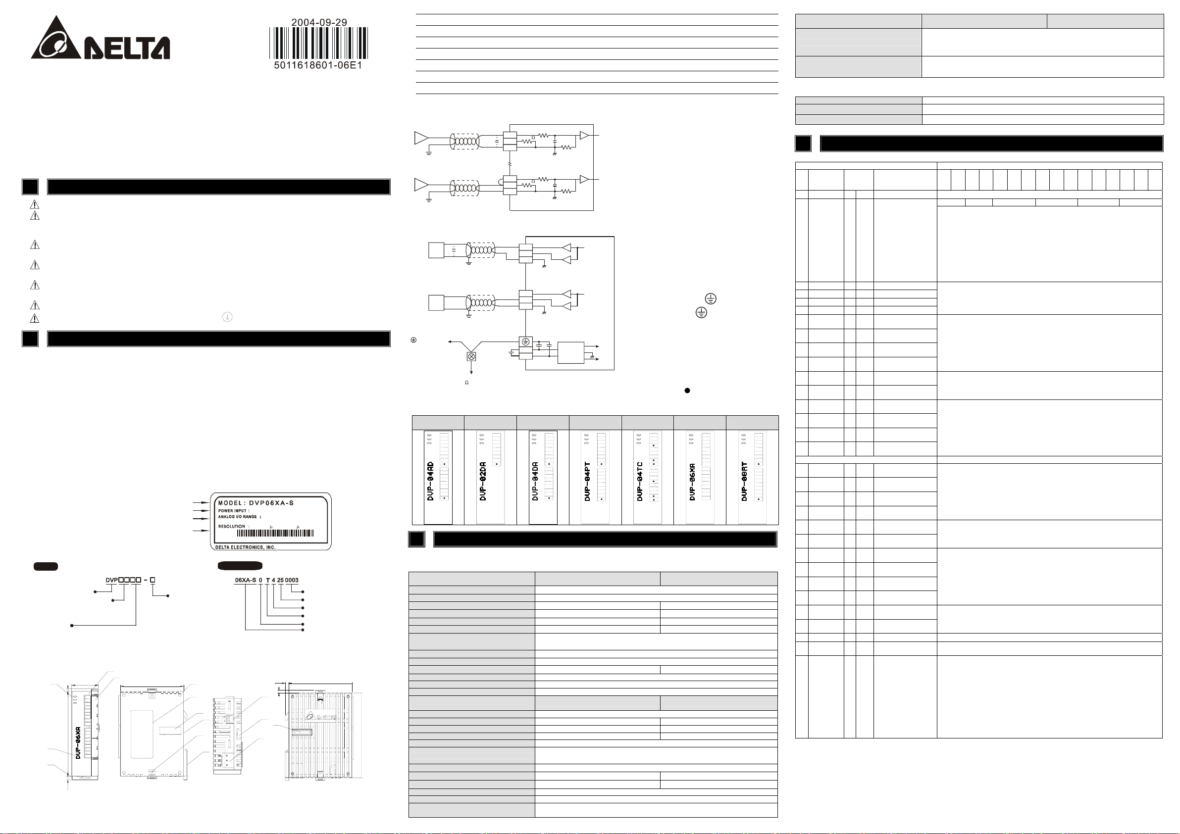
DVP06XA-S
Analog Input/Output Mixed Module
Instruction Sheet
1
Please carefully read this instruction thoroughly prior to use the DVP06XA-S.
In order to prevent electric shock, do not touch the terminals or conduct any maintenance while
PLC is power on.
to conduct the internal electrical work on PLC.
This is an OPEN-TYPE device and already certified to meet the IEC 61131-2 (UL 508) safety
requirements when installed in an enclosure.
DVP06XA-S must be placed in an environment away from high temperatures, high humidity,
exceessive vibration, corrosive gases, liquids, airborne dust, and metallic particles.
Do not apply AC power to any of the input/output terminals, or it may cause permanent damage to
the DVP06XA-S.
Do not touch the internal circuit for at least 1 minute after the power supply is Off.
Make sure that DVP06XA-S is properly grounded , to avoid any electromagnetic noise.
2
2.1 Model Explanation and Peripherals
Thank you for choosing DELTA DVP Series PLC. The DVP06XA-S allows the connection of four
analog inputs and 2 groups 12 bits digital outputs (voltage/current). The PLC converts the input
into a 12-bit digital signal and the output into a 2 points analog signal, which then are manipulated
by using TO and FROM commands in the ladder logic program. There are 49 Controlled
Registers (CR, each register has 16-bit) in each module. The DVP06XA-S series can read/write
the data by using commands FROM / TO via DVP-PLC SS/SA/SX MPU program.
Software version of DVP06XA-S analog input/output mixed module can be updated via RS-485.
Power supply and main processing units are sold separately.
Users can select input from voltage or current via wiring. Voltage input range is ±10V DC
(resolution is 5 mV) and current is ±20mA (resolution is 20 µA).
Users can select output from voltage or current via wiring. Voltage output range is 0V ~ +10V DC
(resolution is 2.5 mV) and current is 0mA ~ 20mA (resolution is 5 µA).
Nameplate Explanation
Model Explanation
Model
Product Series
In put + Ou tput p oin ts
Model type
AD: Analog input module
DA: Analog output module
PT: Platinu m temperature senso rs (PT-100)
TC: Thermocoupl e sensors (Type J/K)
2.2 Product Profile and Outline
1
3.00
90.00
2
3
4.00
DO NOT open the PLC. Only qualified staff or associated person is allowed
Production model
Power input spec.
Analog I/O module spec.
Barcode and serial
number version
4
25.20
5
60.00
IN
V+
C
I+
H
1
COM
V+
C
I+
H
2
COM
V+
C
I+
H
3
COM
V+
C
I+
H
4
COM
V+
C
I+
H
5
COM
V+
C
I+
H
6
COM
OUT
WARNING
INTRODUCTION
20.4VDC ~ 26.4VDC
5mV or 20 A / 2.5mV or 5 A
06XA-S0 T325003VX.X
Serial Number
S: for SS series MPU
P: for EP series MPU
H: f or EH s eries MPU
XA: Analog input/output mi xed module
RT: Resist or Thermoco uple
HC: Input module of high-speed counter
PU: single axis positioning unit
6
7
8
10
9
3
UNIT:mm
13
- 10V ~ + 10V or - 20mA ~ + 20mA
/ 0V ~ + 10V or 0mA ~ +20mA
MADE IN XXXXXX
Production seri es
Production we ek
3.4
3.00
11
12
14
Production year (2004 )
Production pla ce (Taoyuan)
Vers ion
Production Model
60.00
90.00
1. Status indicator (Power, RUN and ERROR) 8. Expansion port
2. Model 9. Expansion Clip
3. DIN rail clip 10. DIN rail location (35mm)
4. I/O terminals 11. RS-485 Communication port
5. I/O terminals layout 12. Expansion Clip
6. Expansion hole of the expansion unit 13. DC Power input
7. Specification Label 14. Expansion port
2.3 External Wiring
Voltage input
-10V~+10V
Current input
-20mA~+20mA
AC drive, recorder,
scale valve...
AC drive, recorder,
scale valve...
terminal of
power module
Shielded*1
Shielded*1
voltage output
0V~+10V
*5
shielding cable *1
current output
0mA~20mA
shielding cable *4
class 3 grounding
or less)
(100
CH1
*3
CH4
*2
DC24V
V+
COM
V+
COM
I+
I+
CH5
CH6
250
250
V+
COM
V+
COM
24+
24-
104.7K
104.7K
AG
104.7K
104.7K
AG
I+
I+
CH5
CH6
DC/DC
converter
Note 1: Please isolate analog input and other
CH1
power wiring.
Note 2: If input signal is in current, please
short out between V+ and I+
CH4
terminals.
Note 3: If the noise interference from loaded
input wiring terminal is significant,
please connect a capacitor with
0.1~0.47µF 25V for noise filtering.
Note 4: Please isolate analog output and
other power wiring.
Note 5: If the noise interference from loaded
input wiring terminal is significant,
please connect a capacitor with
0.1~0.47µF 25V for noise filtering.
Note 6: Please connect
terminal and
power module
analog output
module terminal to system earth
+15V
AG
-15V
point and make system earth point
be grounded or connects to machine
cover.
Warning: DO NOT wire to the No function
terminal
2.4 Terminal of analog module layout
DVP04AD-S DVP02DA-S DVP04DA-S DVP04PT-S DVP04TC-S DVP06XA-S DVP08RT-S
+
I+
COM
FG
+
I+
COM
FG
+
I+
COM
FG
+
I+
COM
FG
3
+
I+
COM
FG
+
I+
COM
FG
+
I+
COM
FG
+
I+
COM
FG
+
I+
COM
FG
+
I+
COM
FG
L+
L-
IFG
L+
L-
IFG
L+
L-
IFG
L+
L-
IFG
STANDARD SPECIFICATIONS
L+
L-
SLG
L+
L-
SLG
L+
L-
SLG
L+
L-
SLG
+
I+
COM
+
I+
COM
+
I+
COM
+
I+
COM
+
I+
COM
+
I+
COM
L+
LL+
LL+
LL+
L-
L+
LL+
LL+
LL+
L-
3.1 Specifications
Mixed (06XA) Module, Analog/ Digital (A/D)
Power Supply Voltage
Analog Input Channel 4 channels per module
Analog Input Range
Digital Data Range
Resolution 12 bits (1
Input Impedance
Overall Accuracy
Response Time
Isolation Method There is no isolation between channels.
Absolution Input Range
Digital Data Format 2’s complement of 16-bit, (13 Significant Bits)
Average Function Yes (CR#2~CR#5 can be set and the range is K1~K4096)
Self diagnostic function Self Detection Upper bound and lower bound detection per channel
Mixed (06XA) Module, Digital/Analog (D/A)
Analog Signal Output Channels 2 channel per module
Analog Output Range 0~10V 0~20 mA
Digital Data Range 0~4000 0~4000
Resolution 12 bits (1
Output Impedance 0.5Ω or lower
Overall Accuracy
Response Time
Max. Output Current
Tolerance Carried Impedance
Digital Data Format 2’s complement of 16-bit, (13 Significant Bits)
Isolation Method Isolation between digital and analog circuitry. There is no isolation between channels.
Protection
Module
Module
24 VDC(20.4VDC~28.8VDC) ( –15%〜+20%)
±10V ±20mA
±2000 ±1000
200 KΩ and above 250Ω
±0.5% of full scale of 25℃(77℉)
±1% of full scale during 0~55℃ (32~131℉)
3 ms × channels
±15 V ±32 mA
±0.5% of full scale of 25℃(77℉)
±1% of full scale during 0~55℃ (32~131℉)
3 ms ×Channels
20mA (1KΩ~2MΩ) -
- 0〜500Ω
Voltage output has short circuit protection but long period of short circuit may cause
internal wiring damage and current output break.
Voltage Input Current Input
=5 mV) 11 bits (1
LSB
LSB
=20 µA)
Voltage Output Current Output
=2.5 mV) 12 bits (1
LSB
LSB
=5 µA)
Mixed (06XA) Module, Analog/ Digital (A/D)
Module
Communication Mode (RS-485)
Connect to DVP-PLC MPU in Series
MODBUS ASCII/RTU Mode. Communication baud rate of 4800 / 9600 / 19200 / 38400
/ 57600 / 115200. For ASCII mode, date format is 7Bits, even, 1 stop bit (7 E 1). For
RTU mode, date format is 8Bits, even, 1 stop bit (8 E 1). The RS-485 is disabled when
the DVP06XA-S is connected in series with MPU.
When DVP06XA-S modules are connected to an MPU, the modules are numbered
from 0 - 7. 0 is the closest to the MPU and 7 is the furthest. The Maximum number of
modules is 8 modules and they do not occupy any digital I/O points of the MPU.
Voltage Input Current Input
3.2 Other Specification
Maximum Power Consumption 2W at 24 VDC (20.4VDC~28.8VDC) ( -15 % ~ +20 %)
Environment Condition and Wiring Follow the DVP-PLC MPU.
Static Electricity Prevention All places between terminals and ground comply with the spec.
4 CR(Controlled Register)
DVP06XA-S Analog Input/Output Mixed Module Explanation
CRNoRS-485
Parameter
Address
#0 H 40C8
#2 H 40CA
#3 H 40CB
#4 H 40CC
#5 H 40CD
#6 H 40CE
#7 H 40CF
#8 H 40D0
#9 H 40D1
#10 H 40D2
#11 H 40D3
#12 H 40D4
#13 H 40D5
#14 H 40D6
#15 H 40D7
#16~ #17 Reserved
#18 H 40DA
#19 H 40DB
#20 H 40DC
#21 H 40DD
#22 H 40DE
#23 H 40DF
#24 H 40E0
#25 H 40E1
#26 H 40E2
#27 H 40E3
#28 H 40E4
#29 H 40E5
#30 H 40E6
#31 H 40E7
#32 H 40E8
Latched Register Name b15 b14 b13 b12 b11 b10 b9 b8 b7 b6 b5 b4 b3 b2 b1 b0
R Model type System used, data length is 8 bits (b7~b0). DVP06XA-S model code= H CC
○
R/W Input mode setting
○
R/W CH1 average number
○
R/W CH2 average number
○
R/W CH3 average number
○
R/W CH4 average number
○
R average value of CH1
╳
╳
╳
╳
╳
╳
╳
╳
╳
╳
○
○
○
○
○
○
○
○
○
○
○
○
╳
○
○
input signal
R average value of CH2
input signal
R average value of CH3
input signal
R average value of CH4
input signal
R/W CH5 output signal
value
R/W CH6 output signal
value
R present value of CH1
input signal
R present value of CH2
input signal
R present value of CH3
input signal
R present value of CH4
input signal
R/W To adjust OFFSET
value of CH1
R/W To adjust OFFSET
value of CH2
R/W To adjust OFFSET
value of CH3
R/W To adjust OFFSET
value of CH4
R/W To adjust OFFSET
value of CH5
R/W To adjust OFFSET
value of CH6
R/W To adjust GAIN value
of CH1
R/W To adjust GAIN value
of CH2
R/W To adjust GAIN value
of CH3
R/W To adjust GAIN value
of CH4
R/W To adjust GAIN value
of CH5
R/W To adjust GAIN value
of CH6
R Error status Data register stores the error status, refer to fault code chart for details.
R/W Communication
address setting
R/W Communication baud
rate setting
CH6 CH5 CH4 CH3 CH2 CH1 #1 H 40C9
Input mode setting: (CH1~CH4)
Mode 0: input voltage mode (-10V~+10V). Factory Setting is H0000.
Mode 1: input voltage mode (-6V~+10V).
Mode 2: input current mode (-12mA~+20mA).
Mode 3: input current mode (-20mA~+20mA).
Mode 4: none use.
Output mode setting: (CH5~CH6)
Mode 0: output voltage mode (0V~10V).
Mode 1: output voltage mode (2V~10V).
Mode 2: output current mode (4mA~20mA).
Mode 3: output current mode (0mA~20mA).
The number of readings used for “average” temperature on channels CH1~CH4.
Setting range is K1~K4096 and factory setting is K10.
Display average value of CH1~CH4 input signal
Output value of CH5~CH6, the setting range is K0~K4000. The factory setting is K0
and the unit is LSB.
Display present value of CH1~CH4 input signal
Offset setting of CH1~CH4. Factory setting is K0 and unit is LSB.
Voltage input: setting range is K-1000 ~K1000
Current input: setting range is K-1000 ~K1000
Offset setting of CH5~CH6. Factory setting is K0 and unit is LSB.
The setting range is K-2000~K2000
GAIN setting of CH1~CH4. Factory setting is K1000 and unit is LSB.
Voltage input: setting range is K-800 ~K4000
Current input: setting range is K-800 ~K2600
GAIN setting of CH5~CH6. Factory setting is K2000 and unit is LSB.
The setting range is K-1600~K8000
RS-485 communication address.
Setting range is K1~K255 and factory setting is K1
Communication baud rate (4800, 9600, 19200, 38400, 57600 and 115200 bps).
For ASCII mode, date format is 7Bits, even, 1 stop bit (7 E 1). For RTU mode, date
format is 8Bits, even, 1 stop bit (8 E 1).
b0: 4800 bps (bit/sec)
b1: 9600 bps (bit/sec). (factory setting)
b2: 19200 bps (bit/sec).
b3: 38400 bps (bit/sec).
b4: 57600 bps (bit/sec).
b5: 115200 bps (bit/sec).
b6~b13: Reserved.
b14: switch between low bit and high bit of CRC code (only for RTU mode)
b15: RTU mode.
#33 H 40E9 ○ R/W Reset to factory
#34 H 40EA ○ R Software version Display software version in hexadecimal. Example: H 010A = version 1.0A.
#35~#48 System used
○ means latched.
╳ means non-latched.
R means can read data by using FROM command or RS-485.
W means can write data by using TO command or RS-485.
LSB (Least Significant Bit): 1. Voltage input: 1
setting and set
characteristics
adjustable priority
b15 b14 b13 b12 b11 b10 b9 b8 b7 b6 b5 b4 b3 b2 b1 b0
CH6 CH5 CH4 CH3 CH2 CH1
Example: Setting of CH1
1. When b0=0, user can set OFFSET and GAIN value of CH1 (CR#18, CR#24).
When b0=1, inhibit user to adjust OFFSET and GAIN value of CH1 (CR#18,
CR#24).
2. b1 means if characteristic register is latched. b1=0 (factory setting, latched), b1=1
(not latched).
3. b2: Set to 1 and PLC will be reset to factory settings.
The setting of CH5~CH6, give CH5 setting for example:
b13, b12:
00: can be adjusted, latched.
01: can be adjusted, non-latched.
10: inhibit adjust.
11: reset to factory settings and clear b12, b13 to 0.
3. Voltage output: 1
=10V/2000=5mV. 2. Current input: 1
LSB
=10V/4000=2.5mV. 4. Current output: 1
LSB
=20mA/1000=20µA.
LSB
=20mA/4000=5µA.
LSB
Explanation:
1. CR#0: The PLC model type.
2. CR#1: b11~b0 are used to set 4 internal channels working mode of analog input module (AD).
b12~b15 are used to set 2 channels working mode of analog output module (DA). Every channel
has four modes that can be set individually. For example: if setting CH1 to mode 0 (b2~b0=000),
CH2 to mode 1(b5~b3=001), CH3: mode2 (b8~b6=010), CH4: mode 3(b11~b9=011), b0~b11
need be set to H688. If setting CH5: mode 2 (b13~b12=10), CH6: mode 1 (b15~b14=01),
b12~b15 need be set to H5. The factory setting is H0000.
3. CR#2 ~ CR#5: Used to set the number of piece of input readings for the average temperature
calculation. The available range is K1~K4096 and factory setting is K10.
4. CR#6 to CR#9: The average value of temperature in ℃. Temperature is calculated by averaging
multiple temperature readings. Example: If CR#2 is 10, the temperature in CR#6 will be the
average of the last 10 readings on CH1.
5. CR#10 ~ CR#11 are used to set the output value of CH5 and CH6. The setting range is
K0~K4000. The factory setting is K0 and unit is LSB.
6. CR#12 ~ CR#15: used to save the present value of input signal of CH1~CH4.
7. CR#16, CR#17, CR#28, CR#29 are reserved.
8. CR #18~ CR #21: used to adjust the OFFSET value of CH1~CH4 if analog input either in voltage
or in current is 0 after it converts from analog to digital. Voltage setting range:
-5V~+5V(-1000
~+1000
LSB
). Current setting range: -20mA~+20mA (-1000
LSB
~+1000
LSB
LSB
).
9. CR #22~ CR #23: used to adjust the OFFSET value of CH5~CH6 if analog input either in voltage
or in current is 0 after it converts to digital. Factory setting is K0, and the unit is
range is -2000~+2000. Voltage setting range: -5V~+5V(-2000
range: -10mA~+10mA (-2000
~+2000
LSB
LSB
).
~+2000
LSB
. The setting
LSB
). Current setting
LSB
10. CR #24~ CR #27: used to adjust the GAIN value of CH1~CH4. The value of analog input either
in voltage or in current after it was converted to digital based upon full scale of 4000. Voltage
setting range: -4V~+20V(-800
~+2600
(voltage) or +200
). But it needs to notice that GAIN VALUE - OFFSET VALUE = +200
LSB
~+1600
LSB
~+4000
LSB
(current). If the value difference comes up small (within range),
LSB
). Current setting range: -16mA~+52mA (-800
LSB
~+3000
LSB
LSB
LSB
the output signal resolution is then slim and the variation is definitely larger. On the contrast, if
the value difference exceeds the range, the output signal resolution becomes larger and the
variation is definitely smaller.
11. CR #28~ CR #29: used to adjust the GAIN value of CH5~CH6. The value of analog input either
in voltage or in current after it converts to digital based upon full scale of 2000. Voltage setting
range: -4V~+20V(-1600
~+8000
LSB
Please be noticed that GAIN VALUE – OFFSET VALUE = +400
). Current setting range: -8mA ~+40mA (-1600
LSB
~+6000
LSB
LSB
~+8000
LSB
LSB
(voltage or current).
If the value difference comes up small (within range), the output signal resolution is then slim
and the variation is definitely larger. On the contrast, if the value difference exceeds the range,
the output signal resolution becomes larger and the variation is definitely smaller.
12. CR#30 is the fault code. Please refer to the chart below.
Fault description Content b15~b8 B7 b6 b5 b4 b3 b2 b1 b0
Power source abnormal
(Low voltage alarm)
User setting D/A output
exceeds range
Setting mode error K4(H4) 0 0 0 0 0 1 0 0
Offset/Gain error K8(H8) 0 0 0 0 1 0 0 0
Hardware malfunction K16(H10) 0 0 0 1 0 0 0 0
Digital range error K32(H20) 0 0 1 0 0 0 0 0
Average times setting error K64(H40) 0 1 0 0 0 0 0 0
Command error K128(H80)
Note: Each fault code will have corresponding bit (b0~b7). Two or more faults may happen at the same time. 0 means
normal and 1 means having fault.
K1(H1) 0 0 0 0 0 0 0 1
K2(H2) 0 0 0 0 0 0 1 0
Reserved
1 0 0 0 0 0 0 0
13. CR#31: RS-485 communication address. Setting range is 01~255 and factory setting is K1.
14. CR#32: RS-485 communication baud rate: 4800, 9600, 19200, 38400, 57600 and 115200.
b0:4800bps, b1:9600bps (factory setting), b2:19200bps, b3:38400 bps, b4:57600 bps,
b5:115200 bps, b6~b13: Reserved, b14: switch between low bit and high bit of CRC code (RTU
mode only) b15: ASCII / RTU mode. For ASCII mode, date format is 7Bits, even, 1 stop bit (7 E
1). For RTU mode, date format is 8Bits, even, 1 stop bit (8 E 1).
15. CR#33 is used to set the internal function priority. For example: characteristic register. Output
latched function will save output setting in the internal memory before power loss.
16. CR#34: software version.
17. CR#35~ CR#48: system used.
18. The corresponding parameters address H 40C8~H 40F9 of CR#0~CR#48 will allow user to
read/write data via RS-485.
A. Baud rate can be 4800, 9600, 19200, 38400, 57600, 115200bps.
B. MODBUS communication protocol can be either in ASCII or in RTU mode. For ASCII mode,
date format is 7Bits, even, 1 stop bit (7 E 1). For RTU mode, date format is 8Bits, even, 1
stop bit (8 E 1).
C. Function code: 03H read data from register.
06H write one WORD into register.
10H write multiple WORD into register.
5
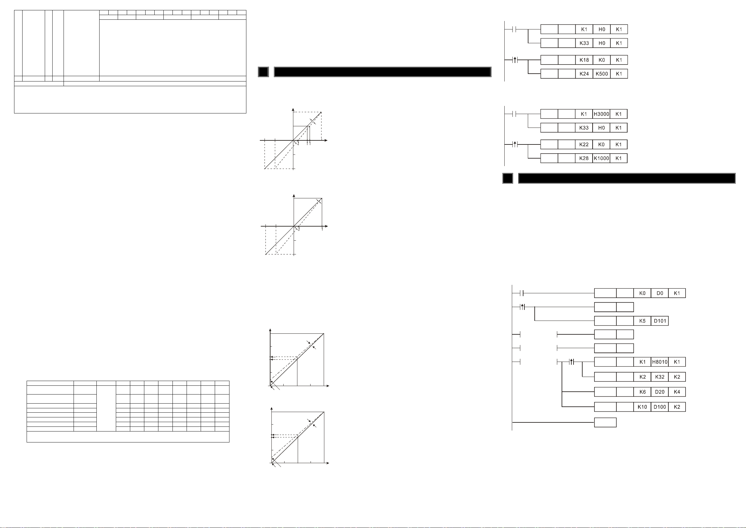
Adjust A/D Conversion Characteristic Curve
5.1 Adjust A/D Conversion Characteristic Curve of CH1~CH4
Voltage input mode
Current input mode:
input mode. Users can adjust conversion characteristic curve by changing OFFSET values
(CR#18~CR#21) and GAIN values (CR#24~CR#27) depend on application.
20µA.
-6V-10V
-12mA-20mA
digital output
+2000
+1000
0
Digital output
+2000
0
OFFSET
-1000
-2000
4mA
OFFSET
-2000
Mode 0
6V5V2V
GAIN
Mode 3
Mode 1
10V
Mode 2
GAIN
Mode 0 of CR#1: GAIN=5V(1000
Mode 1 of CR#1: GAIN=6V(1200
Voltage
input
GAIN:
OFFSET:
Voltage input value when digital output is 4000.
Setting range is -4V~+20V(-800
Voltage input value when digital output is 0.
Setting range: -5V~+5V(-1000
GAIN-OFFSET: Setting range is +1V~+15V (+200
Mode 2 of CR#1: GAIN = 20mA(1000
Mode 3 of CR#1: GAIN = 20mA(1000
GAIN:
Current input value when digital output is +4000.
Setting range is -20 mA~+20mA (-1000
Current
Input
20mA
OFFSET:
+1000
Current input value when digital output value is
LSB
)
0. Setting range is-16mA ~+52mA (-800
GAIN-OFFSET:
+2600
Setting range is +4mA ~ +32mA (200
+1600
LSB
LSB
)
)
), OFFSET=0V (0
LSB
), OFFSET=2V (400
LSB
LSB
), OFFSET=4mA (200
LSB
), OFFSET=0mA (0
LSB
LSB
~ +4000
LSB
~ +1000
~ +3000
LSB
LSB
).
LSB
LSB
LSB
~
).
LSB
)
LSB
LSB
LSB
).
LSB
~
~
Use the chart above to adjust A/D conversion characteristic curve of voltage input mode and current
LSB (Least Significant Bit): 1. voltage input: 1
=10V/2000=5mV. 2. current input: 1
LSB
=20mA/1000=
LSB
5.2 Adjust D/A Conversion Characteristic Curve of CH5~CH6
Voltage output mode
Voltage output
10V
mode 1
).
6V
GAIN
5V
2V
0
OFFSET
Current output mode:
Current output
20mA
mode 0
+2000 +4000
Mode 2
Mode 0 of CR#1: GAIN = 5V(2000
Mode 1 of CR#1: GAIN = 6V(2400
), OFFSET=0V (0
LSB
), OFFSET=2V (800
LSB
GAIN: Voltage output value when digital input is K2000.
Setting range is -4V~+20V(-1600
LSB
OFFSET: Voltage output value when digital input is K0.
Setting range: -5V~+5V(-2000
GAIN-OFFSET:
Digital
input
Setting range is +1V~+15V(+400
Mode 2 of CR#1: GAIN = 12mA(2400
Mode 3 of CR#1: GAIN = 10mA(2000
),OFFSET=4mA (800
LSB
), OFFSET=0mA (0
LSB
~ +2000
LSB
LSB
)
LSB
).
LSB
~+8000
LSB
~ +6000
LSB
LSB
).
LSB
LSB
).
GAIN: Current output value when digital input value is
K2000. Setting range is -8mA ~+40mA (-1600
~+8000
LSB
).
12mA
10mA
GAIN
Mode 3
OFFSET: Current output value when digital input is K0.
Setting range is -10mA ~+10mA (-2000
4mA
0
OFFSET
+2000 +4000
GAIN-OFFSET:
Digital
input
~+2000
Setting range is +2mA~+30mA (+400
~+6000
LSB
LSB
).
LSB
)
Use the chart above to adjust D/A conversion characteristic curve of voltage output mode and
current output mode. Users can adjust conversion characteristic curve by changing OFFSET values
(CR#14~CR#15) and GAIN values (CR#18~CR#19) depend on application.
LSB (Least Significant Bit): 1. voltage output: 1
2. current output: 1
=10V/4000=2.5mV.
LSB
=20mA/4000=5µA.
LSB
5.3 Program Example for Adjusting A/D Conversion Characteristics Curve
Example: setting OFFSET value of CH1 to 0V(=K0
M1002
K0TO
) and GAIN value of CH1 to 2.5V(=K500
LSB
Write H0 to CR#1 of analog input module
no. 0 and set CH1 to mode 0 (voltage input
-10V~+10V)
K0TO
X0
K0TO
K0TO
Write H0 to CR#33 and allow to adjust
characters of CH1.
When X0 switches from Off to On, K0
OFFSET value will be wrote in CR#18 and
K500
CR#24.
of GAIN value will be wrote in
LSB
5.4 Program Example for Adjusting D/A Conversion Characteristics Curve
Example: set OFFSET value of CH5 to 0V(=K0
M1002
K0TO
K0TO
)
X0
K0TO
)
K0TO
) and GAIN value of CH1 to 2.5V(=K1000
LSB
Write H3000 into CR#1 (b12~b15) of
analog input/output module#0. Setting CH5
to mode 3 (current output 0mA~ +20mA).
Write H0 into CR#33 (b12~b15) and allow
CH5, CH6 to adjust characteristics.
When X0 switches from Off to On, K0
OFFSET value will be wrote in CR#22 and
K1000
wrote in CR#28.
of GAIN value K1000
LSB
6 Initial PLC Start-up
).
Lamp display:
1. Upon power-up, the ERROR LED will light for 0.5 seconds the POWER LED will light
continuously.
2. No errors= POWER LED on and ERROR LED off.
Low Voltage error (lower than 19.5V), ERROR LED will blink continuously till the power
supply rises above 19.5V.
3. DVP06XA-S connected to PLC MPU in series = RUN LED on MPU will be lit and A/D LED
or D/A LED should blink.
4. After receiving the first RS-485 command the A/D LED or D/A LED will blink.
5. If the input or output exceeds the upper or lower bounds, then the ERROR LED will blink.
6. When main CPU and expansion unit communicate time-out or abnormal interrupt, LED
ERROR of expansion unit will keep lighting.
Example:
M1000
FROM K0
M1013
INC D100
ADD D101
= K4 000 D 10 0
).
= K4 000 D 10 1
M1002
= HCC D0
RST
D100
D101
RST
TO K0
)
TO K0
FROM K0
).
LSB
TO K0
END
Explanation:
LSB
Reading the model type of expansion module K0 (should be HCC for DVP06XA-S model type).
If the model type is DVP06XA-S, set the input mode is (CH1, CH3, CH4)= mode 0, (CH2)= mode 2,
and set the output mode is (CH5)=mode 0, (CH6)=mode 2.
Setting the average number of CH1 and CH2 are K32.
Reading the input signal average value of CH1~CH4 (4 data) from CR#6~CR#9 and save in
D20~D23.
In each second, D100 will increase K1 and D101 will increase K5. When the value of D100 and
D101 are K4000, it will clear to 0.
Writing the output setting value of D100 and D101 into CR#10 and CR#11. The analog output value
of CH5~CH6 will change with the value of D100 and D101.
LSB
LSB
).
).
LSB
of
LSB
of
LSB
will be
 Loading...